-4
Demonstration System for A Low Power Video
Compression Integrated Circuit
by
Charatpong Chotigavanich
Submitted to the Department of Electrical Engineering and Computer
Science
in partial fulfillment of the requirements for the degree of
Master of Engineering
at the
MASSACHUSETTS INSTITUTE OF TECHNOLOGY
February 2000
@
Charatpong Chotigavanich, MM. All rights reserved.
The author hereby grants to MIT permission to reproduce and
distribute publicly paper and electronic copies of this thesis
in whole or in part.
A uthor ...
document ftr
MASSACHUSETTS NSTITUTE OFTECHNOLOGYJUL 2
7 2000
L:BARIESDepartment of Electrical Engineering and Computer Science
January 20, 2000
C ertified by ...
.
.
. ...
Anantha P. Chandrakasan
Associate Profeseor~of Electrical Engineering
Th0si§)SupervisorAccepted by...
...
Demonstration System for A Low Power Video Compression
Integrated Circuit
by
Charatpong Chotigavanich
Submitted to the Department of Electrical Engineering and Computer Science on January 20, 2000, in partial fulfillment of the
requirements for the degree of Master of Engineering
Abstract
This thesis demonstrates a low power video compression integrated circuit which consumes ultra low power. The system digitizes analog video signal and compresses it using the video compression integrated circuit which utilizes wavelet transform and zero tree coding algorithm to achieve high compression ratio and ultra low power. The compressed data is then sent to a PC where it is decoded and played as a movie in real time.
Thesis Supervisor: Anantha P. Chandrakasan Title: Associate Professor of Electrical Engineering
Acknowledgments
My thesis could not be accomplished without the following people.
First of all, I would like to thank Prof. Anantha Chandrakasan for agreeing to supervise this thesis. I greatly appreciate his help, suggestions, and also patience. Throughout the term, he has been an excellent consultant who gives me advices on not only academic issues but also life after school in general.
I also would like to thank Rex Min for his great assistance with almost everything. I learned a lot from his past work and his hand-on experiences. He has been a great instructor who leaves his desk at his busiest time of the day just to help me figure out some minor bugs. This thesis would not even exist without him.
I thank Jim MacArthur. He is the guy who actually educated me and taught me the real-world engineering lessons. In addition, Jim is a kind of entertainer whose characters provide a great relief for me in the lab. We share a lot of thoughts about many projects, business, laws, and even startups. If I ever become a millionaire in the future, this is the man I will give my first million to.
I would like to thank Keith Fife for lending me an ISR cable to program CPLDs. He also helped me with the board layout and other circuit problems.
I also thank Thomas Simon for his advices and his patience. Although I was literally an annoyance to him during debugging, he was still calm and continued to help me out.
I am thankful to many people in the lab. They have been very nice and helpful in general. Thanks to: Alice Wang, Raj Amirtharajah, Vadim Gutnik, and Jim Good-man.
I thank all my friends who hang around me when I was not in the lab. Thanks to Sandia Ren, Laurie Qian, and Duncan Bryce who also helped me review this thesis. Thanks to Nuwong Chollacoop for his help in moving my stuff to my new apartment while I was being busy with my thesis.
I owe tremendous gratitude to Preeyanuch Sangtrirutnugul. I could actually say that she is a co-author of this thesis. After all, she stayed up with me until 7am everyday making sure that I wouldn't do something foolish.
Finally, I am grateful to my parents and my family for their continuing support throughout my entire life. Without them, I would not even be writing this thesis.
Contents
1 Introduction 9
1.1 Background on Low-Power Video Processing . . . . 9
1.2 System Overview . . . . 11
1.3 Design Considerations . . . . 11
2 Hardware System 13 2.1 High-Level Block Diagram ... 14
2.2 Image EPROM ... 17
2.3 Input Frame Buffer . . . . 18
2.4 Video Compression Integrated Circuit(EZW Chip) . . . . 25
2.5 EZW Output Frame Buffer . . . . 29
2.5.1 Bit Packing Finite State Machine . . . . 31
2.5.2 Synchronizer Finite State Machine . . . . 34
2.5.3 Read/Write Buffer Switch . . . . 35
2.6 Parallel Port Interface . . . . 35
2.7 Complex Programmable Logic Devices(CPLD) . . . . 40
3 Software System 42 3.1 Direct Memory Access Device Driver . . . . 43
3.2 D ecoder . . . . 43 3.3 Video Player . . . . 44 3.4 User Interface(UI) . . . . 45 4 System Implementation 47 4.1 Hardware System . . . . 47 4.2 Software System . . . . 49 5 System Performance 52 6 Conclusion and Future Improvement 54 6.1 Conclusion . . . . 54
6.2 Ideas for the Future . . . . 55
Bibliography 56
B VHDL Code 64
B.1 VHDL Code for CPLD 1 ... 64
B .I.1 i2c.vhd . . . . 64
B .I.2 ntsc.vhd . . . . 73
B.I.3 ezw-sram -drive. vhd . . . . 76
B .I.4 top-a.vhd . . . . 80 B.2 VHDL Code for CPLD 2 . . . . 83 B.2.1 sram-switch.vhd . . . . 83 B.2.2 ezw-out.vhd . . . . 86 B.2.3 parallel -sram. vhd . . . . 91 B.2.4 top-b.vhd . . . . 95 C Decoder Code 100 C-1 Decoder Code in C . . . . 100 C .1.1 StdA fx.h . . . . 100 C-1.2 StdAfx.cpp . . . . 101 C.1.3 vdodm a3.h . . . . 101 C.1.4 vdodma3.cpp . . . . 101 C .1.5 resource.h . . . . 141 C.1.6 m akefrm -c . . . . 142
List of Figures
2-1 Overview block digram of the hardware system . . . . 13
2-2 Timing diagram of output signals from Bt829A . . . . 16
2-3 An example of a buffer using a one-port SRAM . . . . 19
2-4 A mechanism used to prevent image corruption . . . . 20
2-5 Finite state machine of the left control logic module . . . . 21
2-6 Finite state machine of the right control logic module . . . . 22
2-7 How a frame is loaded . . . . 24
2-8 Addressing scheme of the input buffer . . . . 24
2-9 Combinational logic which controls the tri-state outputs of SRAM buffer and image EPROM . . . . 25
2-10 Timing Diagram of Input Signals to Video Compression Integrated C ircuit . . . . 26
2-11 Timing Diagram of Output Signals from Video Compression Integrated C ircuit . . . . 28
2-12 64MHz to 500KHz clock divider . . . . 29
2-13 Schematic Diagram of the Output Frame Buffer Controller . . . . 30
2-14 Bit Packing Finite State Machine . . . . 31
2-15 Bit Storage Format . . . . 32
2-16 An alternative of how to store a bit . . . . 33
2-17 State diagram of parts of Read/Write Buffer Switch . . . . 34
2-18 Schematic Diagram of parts of Read/Write Buffer Switch . . . . 36
2-19 Timing Diagram of the Parallel Port Protocol in ECP mode. . . . . . 37
2-20 State diagram of finite state machine that controls the parallel port interface . . . . 39
2-21 Logic blocks in the first CPLD . . . . 40
2-22 Logic blocks in the second CPLD . . . . 41
3-1 Block Diagram of the Software System . . . . 42
3-2 Double frame buffer . . . . 45
3-3 The Working System . . . . 46
4-1 The front side of the unpopulated PCB . . . . 48
4-2 The back side of the unpopulated PCB . . . . 49
4-3 The Finished PCB with all components in place . . . . 50 A-1 Schematic Diagram of Analog to Digital Converter and Its Control Logic 58
A-2 Schematic diagram of EZW chip . . . . 59
A-3 Three instruction EPROMs for the EZW chip . . . . 59
A-4 Schematic diagram of the image EPROM . . . . 60
A-5 Schematic diagram of the SRAM buffer and its control logic modules 61 A-6 Schematic Diagram of i2c programmer . . . . 61
A-7 Schematic Diagram of Output Frame Buffer . . . . 62
A-8 Schematic Diagram of Parallel Port Interface . . . . 62
List of Tables
2.1 Bt829A pin descriptions . . . . 15 2.2 Pin descriptions of the EZW chip . . . . 27 2.3 Mapping Between Centronics pinouts and D-SUB pinouts . . . . 38 5.1 The relationship between the number of frames decoded and the latency 53 5.2 The performance of this EZW video chip . . . . 53
Chapter 1
Introduction
1.1
Background on Low-Power Video Processing
Video compression has been an important research topic for the past several years, and a large number of algorithms and hardware devices were developped as a result. Usually these algorithms and hardware devices target better quality, and more com-pression ratio. A lot of algorithms developed for video comcom-pression are for desktop computers where the amount of power required for computation is not really a ma-jor concern. However, as portable applications become widespread, researchers have become aware of power consumption as an important issue. The need for low-power algorithms and hardware become inevitable. And for portable video devices, data compression is one obvious way of saving power. Data compression reduces not only the capacity required for data storage, but also power consumption because there is less data to be transmitted. Wireless camera is an evident example of how a system can benefit from data compression.In this case, the RF transmitter obviously con-sumes less power in sending smaller amount of data through a wireless network.Thus, a lot of algorithms for video data compression have been developed such as JPEG, MPEG, etc. Most algorithms fall under the category of "lossy compres-sion" where image quality is reduced to compensate for the compression ratio gain.
an algorithm is implemented in hardware actually accounts for most of the power consumption.
There are a lot of general purpose processors(GPP) which are capable of running virtually any of the video compression algorithms. But those GPPs usually consume too much power, and portable devices which utilize such processors, eg. laptop com-puters, usually have large batteries and require a long re-charging time almost daily. Therefore, a low-power integrated circuit is a necessity for this video application.
This thesis demonstrates the performance of a "wavelet transform and zero-tree coding" video compression integrated circuit which requires low power consumption and yields high compression ratio. Designed by Thomas Simon as a part of his PhD thesis[4], this video compression integrated circuit uses the wavelet transform and zero-tree coding algorithm[2] to compress and encode digital video signal. The chip is a massively parallel SIMD processor which utilizes wavelet transform and zero tree coding algorithm to compress and encode digital video data. The parallel nature of the processor is key to achieving low power. When parallelism is introduced into a system, the computation process can be done faster. But for an application whose input or output is stream data with a fixed rate of arrival or departure, the speed-up from parallelism is a waste. As a result, by reducing the power sspeed-upply voltage, the computation time can be lengthened just enough for a system with parallelism to meet the required rate. At the lower power supply voltage, the circuit consumes less power. This technique means that the speed-up can save some power consump-tion. Using this technique, the core of this video compression chip operates at 1.5V, consumes 300-400/LW, and yields compression ratio up to 300:1 for acceptable image quality.
1.2
System Overview
The system presented in this thesis will be a useful tool to demonstrate how much power can be saved from the parallel architecture. The function of this system is to digitize and compress a real-time video signal from a camera, send the data to a PC, decode the data and finally, play the video signal on the PC's monitor. The entire process can be performed in real-time with a few seconds of frame latencies.
This demonstration system comprises of hardware and software. The hardware system is a 7.5"x7.5" printed circuit board with a video compression integrated circuit and several other electrical components including the "wavelet transform and zero-tree coding" video compression integrated circuit. The board handles NTSC signal digitization, digital video compression, and data transmission to a PC.
The software part of this demonstration is developed for Microsoft Windows plat-form. The software runs on Windows 95, Windows 98, and Windows NT. The soft-ware is responsible for data reception from the board, data decompression, and video playback.
1.3
Design Considerations
"
Ease of Use. Since this system will be frequently employed to demonstrate the performance of the video compression integrated circuit, the system has to be easy to operate. The hardware is designed to have a few controls on the circuit board, and the user-interface of the software is developed to be user-friendly. " Ease of Debugging. The system is designed with modularity. There areseveral small modules in this circuit and they are abstracted away from one another. The interface between each module is consistent throughout the design
probes for debugging. The electrical components on the board are placed on sockets so that they can be changed if damaged.
* Extensibility. This demonstration can potentially be a submodule of another system, such as a wireless camera; therefore, it has to be extensible. The circuit board utilizes surface-mounted complex programmable logic devices(CPLD) which can be programmed on-board. These CPLDs provide great flexibility and extensibility to modify the code in the future. The circuit also uses EPROMs for data storage so the contents can be changed if necessary.
* Small Printed Circuit Board Area. The area of the printed circuit board is minimized. All electrical components are placed tightly next to one another to achieve minimal board area.
Chapter 2
Hardware System
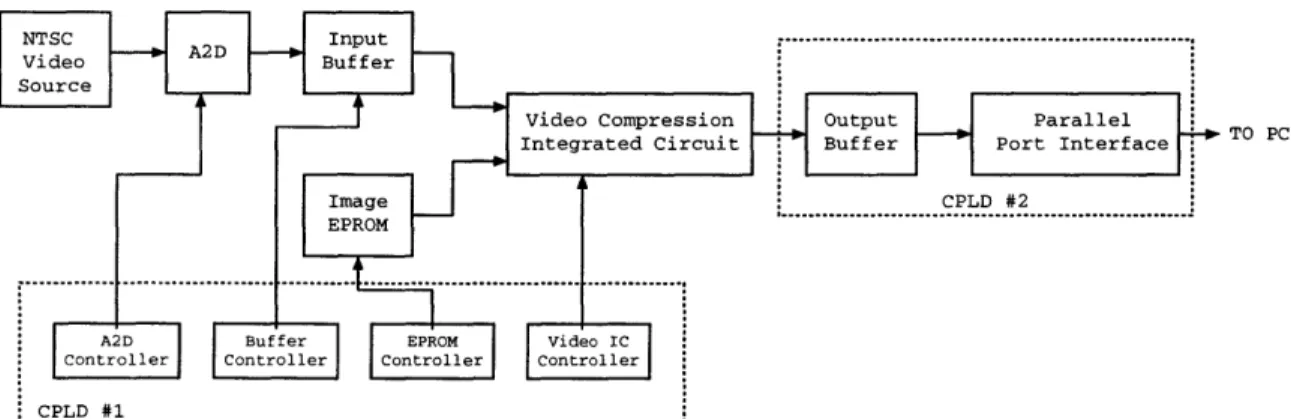
This chapter discusses the hardware part of this system which handles NTSC signal digitization, digital video compression, and data transmission to a PC. The architec-ture of the system is divided into several circuit modules. The interface specifications between each modules are kept consistent throughout the design process so that an internal change of one module would not effect the others. The modular design of the hardware reduces the possibility of bugs and greatly speeds up the design process.
NTSC A D Input .---.
Video Buffer Source
Video Compression Output Parallel
Integrated Circuit Buffer Port Interface TOC
EPROM
A2D Buffer EPROM Video IC
Controller Controller Controller Controller
F rCPLD 21
2.1
High-Level Block Diagram
Figure 2-1 illustrates a high-level block digram of the hardware system. The system can receive two sources of video input. One is analog video signal from an NTSC video source, and the other is digital video signal programmed on an EPROM. For analog video signal input, the signal is digitized into digital video stream. This video stream is buffered and appropriately formatted for further processing. On the other hand, the digital video input from the EPROM does not require analog-to-digital conversion and frame buffering, and thus can be processed right away. Selected by a controller, one of these two sources is then passed on to the video compression integrated circuit, where the compression and encoding operations take place. The output, as a stream of bits, is again buffered before it is sent to a PC through a parallel port interface circuit which governs the transmission process.
The A2D converter receives NTSC signal from an NTSC source and produces an 8 bit gray-scale image that can be further processed. This NTSC source can be any device, such as video player and video camera, which provides standard NTSC video signal. Because NTSC is a widespread standard in North America, using the NTSC interface allows this system to receive a variety of video input devices.
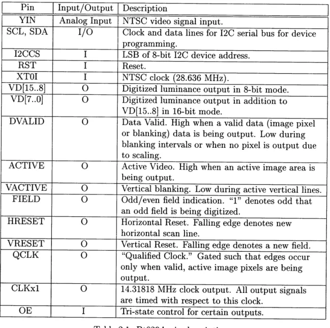
The design of the A2D module in this system is a slightly modified version of the one from [3]. More details about this Bt829A can be found in [3] and [8].
Manufactured by Rockwell Semiconductor, the Bt829A chip is a widely used video decoder in several video appliances including personal computers. In addition to its ease of use, the chip supports a variety of video signal formats, such as NTSC and PAL. It is also capable of adjusting frame size, frame resolution, and zooming. In short, this chip is very powerful, versatile, and cheap. Table 2.1, replicated from [3], shows the pin descriptions of this chip.
Pin Input/Output Description
YIN Analog Input NTSC video signal input.
SCL, SDA
I/O
Clock and data lines for 12C serial bus for device programming.I2CCS I LSB of 8-bit 12C device address.
RST I Reset.
XTOI I NTSC clock (28.636 MHz).
VD[15..8] 0 Digitized luminance output in 8-bit mode.
VD[7..0] 0 Digitized luminance output in addition to
VD[15..8] in 16-bit mode.
DVALID 0 Data Valid. High when a valid data (image pixel or blanking) data is being output. Low during blanking intervals or when no pixel is output due
to scaling.
ACTIVE 0 Active Video. High when an active image area is
being output.
VACTIVE 0 Vertical blanking. Low during active vertical lines. FIELD 0 Odd/even field indication. "1" denotes odd that
an odd field is being digitized.
HRESET 0 Horizontal Reset. Falling edge denotes new horizontal scan line.
VRESET 0 Vertical Reset. Falling edge denotes a new field. QCLK 0 "Qualified Clock." Gated such that edges occur
only when valid, active image pixels are being
output.
CLKx1 0 14.31818 MHz clock output. All output signals
are timed with respect to this clock.
OE I Tri-state control for certain outputs. Table 2.1: Bt829A pin descriptions
VD[15. .0]
DVALID
ACTIVE
CLKxl
a) Pixels are valid when both DVALID and ACTIVE are both high. All signals are synchronized to CLKxl which is 14.31818MHz. The falling edge of DVALID signifies
the new field is being output.
HRESET
DVALID
ACTIVE
b) This timing diagram, the zoomout diagram of (a), displays the relationship between HRESET, DVALID, and ACTIVE.
VRESET
HRESET
VACTIVE
C) This timing diagram, the zoomout diagram of (b), shows the relationship between VRESET, HRESET, and VACTIVE
The Bt829A digitizes analog NTSC signal from input YIN. Synchronized to CLKxl, the digital output VD[15..8] and VD[7..0] represent luminance and chrominance re-spectively. Because this system only needs 8 bits of data, the chrominance information is ignored. So only VD[15..8] is used as displayed in Figure A-1. The timing diagram of the output signal is illustrated in Figure 2-2.
Since this Bt829A requires programming upon startup, a control logic provides programming interface to the chip using 12C protocol[7]. This control logic is im-plemented on a CPLD to allow flexible design and ease of debugging. The control logic is a finite state machine which programs the Bt829A on SCL and SDK pins with desired parameters. The implementation of the FSM was obtained from [3] with some parameters adjusted for this demonstration system. There are several sets of these parameters which yield 128x128 output frames, and each set of parameters results in different image size and quality.
In this demonstration system, two sets of parameters were tested. The first param-eter set programs the Bt829A to digitize a frame at resolution 256x256, and then scale down to 128x128 vertically and horizontally. This method creates jagged horizontal lines on every frame because the Bt829A does not scale interlaced frames very well. The other set of parameters eliminated this problem by using non-interlace mode or decimating the even fields of the digitized frame, so the frame then has 128x256 video resolution which is then horizontally scaled down to 128x128. As a result, the second parameter set yields much better and clearer video output.
2.2
Image EPROM
One of the significant challenges in implementing a system that involves real time data is debugging. In a system whose input is real time and nondeterministic, the
not the system is operating correctly from the nondeterministic output because there is nothing to compare the output to. A good method for debugging such a system is to input some test vectors and determine whether the output is as expected. The image EPROM precisely serves this purpose. The schematic diagram of this image EPROM is shown in Figure A-4.
This EPROM stores digital pixels of a video frame. It provides an alternative input in addition to NTSC signal as mentioned in the previous section. The data to be programmed on the EPROM is extracted from an 8-bit 128x128 black-and-white PGM image. The PGM image format is basically an array of raw digital pixels with a string header line which specifies the dimension of the image and level of grey-scale depth. This header line is simply ignored to extract the raw digital pixels. A program written in C is used to convert the PGM image into an appropriate size and format for the EPROM. This program is included in the Appendix.
2.3
Input Frame Buffer
This input frame buffer is simply SRAM used to ensure that pixels are delivered in an appropriate order from the A2D to the video compression chip. Furthermore, to prevent video image corruption, the buffer also handles the rate difference between the output rate of the A2D and the input rate of the video compression chip. The image EPROM, however, does not need this buffer because an EPROM is itself a pre-programmed buffer. The pixels from the image EPROM are sent directly to the video compression chip without buffering. By eliminating the buffering process of the EPROM, the datapath is less complicated and, therefore, more efficient.
There are several ways to implement a buffer. One typical way is as displayed in Figure 2-3. In this implementation, the controller determines when to read and write the the SRAM using two tri-state buffers. The controller cannot read and write
DATA ADDR ADDR R / W R/W WRITE DATA I/o READ DATA Controller SRAM
Figure 2-3: An example of a buffer using a one-port SRAM
simultaneously because there is only data port. Although this implementation might be sufficient, the controller has to operate at very high frequency to keep up with the data rate.
Another way of implementation is to use dual-port SRAM. One port is used solely to write data from A2D, and the other is used to read data. Figure A-5 shows the schematic diagram of the SRAM and its control logic modules. The module on the
left, UCYP_1:D controls the write buffer, and the right one, UCYP-1:E, controls the
read buffer and also the output enable for the image EPROM discussed earlier. To reduce the complexity of the system, both control logic modules are implemented on a CPLD. With this implementation, the buffer can be read and written simultane-ously and the controllers can operate at half of the frequency required for one-port SRAM(or 28.63MHz).
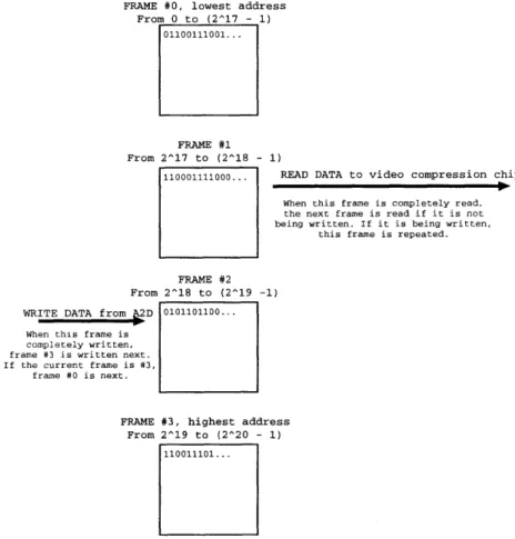
One of the main functions of the buffer is to handle the rate difference between the A2D and the video compression chip. The output rate of the A2D converter is 30 frames per second, but the input rate of the video compression chip is 30.518 frames per second(will be discussed below). If the write address and read address are not controlled, every once in a while both addresses can overlap, thus causing image cor-ruption. Therefore, a control mechanism is necessary to ensure that a frame cannot
FRAME #0, lowest address From 0 to (2^17 - 1)
01100111001...
FRAME #1 From 2^17 to (2^18 - 1)
110001111000... READ DATA to video compression chip
When this frame is completely read, the next frame is read if it is not being written. If it is being written,
this frame is repeated.
FRAME #2 From 2^18 to (2^19 -1)
WRITE DATA from 2D 0101101100... When this frame is
completely written, frame #3 is written next. If the current frame is #3,
frame #0 is next.
FRAME #3, highest address From 2^19 to (2^20 - 1)
110011101 ...
Waiting
Set Address Count=O
Address Count = 16383 (128x128-1) If VRESET = 0 and field = 1 If BANK = 3
BANK = 0
else BANK = BANK + 1
Loading
Figure 2-5: Finite state machine of the left control logic module
the SRAM buffer is divided into 4 memory banks, each capable of storing exactly 1 frame. The read and write control logic modules are designed not to access the same bank simultaneously. Figure 2-4 explains how the mechanism works.
From Figure 2-4, there are four frames, each frame contains 128x128 pixels and occupies address bits 0 - 13 or 214 bytes of space in the SRAM buffer. The highest address bits 14 and 15 are used to identify the number of each frame. The frame being written is always kept at least one frame ahead of the frame being read. Since the reading rate is faster than the writing rate, every 1 or 2 seconds a frame is done reading whereas the next one is still being written. In this case, that read frame has to be repeated to provide more time for the next frame to finish writing. This frame repetition happens only once every few seconds, and it does not have significant effect on the final image. In fact, it is not noticeable at all in the final video output.
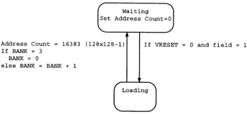
In the schematic diagram in Figure A-5, there are two controllers implemented on a CPLD for design flexibility. The controller on the left of the SRAM is a "write controller" and on the right is a "read controller". The write controller is a simple finite state machine which receives inputs from A2D and writes the data to the SRAM buffer starting from the frame 0. From Figure 2-5, the machine has only 2 states:
Reset
Send reset signal to the video chi
After one clock cycle
Delay Start Idle for 4 cycles
After 4 clock cycles
Waiting
After the left control logic has finished writing a frame
Start Signal
Send a pulse of STARTFRM
to the video chip
One clock cycle
Loading
Looping forever in this state to delive pixels continuously.
The machine repeats a frame when necessary
Figure 2-6: Finite state machine of the right control logic module
delivered from the Bt829A, or when VRESET and FIELD from Bt829A equal to 0 and 1 respectively, the machine proceeds to LOADING state where it starts loading pixel into the SRAM buffer. When all pixels are stored, the machine goes back into
WAITING state and prepares to write to the next frame of the buffer.
Unlike the write controller, the read controller has 2 functions: delivering pixels in a specific order to the video compression chip using the mechanism above to prevent image corruption, and controlling the tri-state outputs of the image EPROM and of the SRAM buffer. The part that delivers pixels is essentially a finite state machine, shown in Figure 2-6. Synchronized to the clock of the video chip, the machine starts
in the RESET state where the video chip is also reset, and then goes to the
DE-LAY START state. The DEDE-LAY START state actually does not do anything but
idle for a few cycles to allow some time for the video chip to become ready. After the DELAY START state, the machine waits in the WAITING state until the write control logic finishes writing the frame 0, then it moves to the START state. In this state, the machine asserts the start signal for the video chip and begins loading pixels continuously in the LOADING state. Looping forever in the LOADING state, the machine repeats loading a frame when the previously described condition occurs.
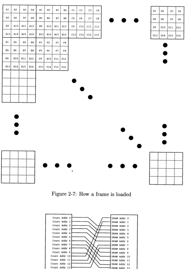
Due to the SIMD architecture of the video chip, frame pixels cannot be loaded in order. Instead, the pixels are loaded as shown in Figure 2-7. One image frame is divided into 1024 4x4 sub-frames. The first pixel of each sub-frame is loaded first one by one, starting from the top left sub-frame(eg. pixel Al, then B1, then C1, ..., then D1, then El, then F1, ...) After that, the next pixel of each sub-frame is loaded(eg.
A2, then B2, then C2, ..., then D2, then E2, then F2, ...) and so on until all the pixels
are loaded. Although this method of pixel loading seems complicated, it is actually easy to implement. The addressing scheme is simply a crossing of the address lines as shown in the Figure 2-8. Using this address crossing scheme, when the Count
Address counts in an increasing order from 0 to 16383, the SRAM is accessed in a
fashion described above automatically.
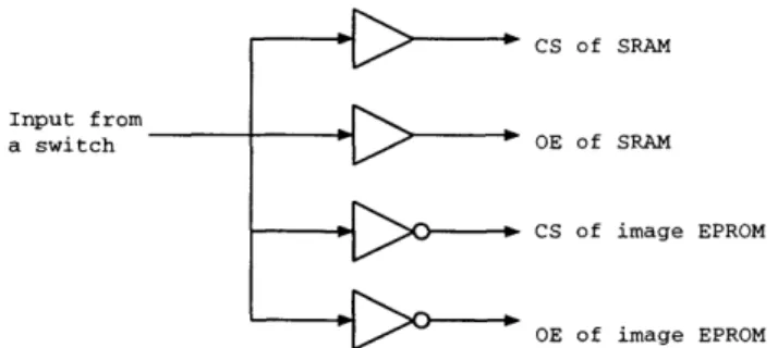
The other function of the read control logic, which controls the tri-state outputs of SRAM and EPROM, is implemented as a set of combinational logic as illustrated in Figure 2-9. Since the output pins of the image EPROM are connected directly to the output ports of the SRAM buffer, this control logic is necessary to prevent bus contention problem. Obtaining input from a switch, the logic simply determines whether the source of data is from the SRAM buffer or the image EPROM.
Al A2 A3 A4 B1 B2 B3 B4 Cl C2 C3 C4
AS A6 A7 A8 B5 B6 B7 B8 C5 C6 C7 C8
A9 A10 All A12 B9 B10 B11 B12 C9 CIO Cl1 C12 A13 A14 A15 A16 B13 B14 B15 B16 C13 C14 C15 C16 El E2 E3 E4
E5 E6 E7 E8
E9 E10 Ell E12
E13 E14 E15 E16
Fl F2 F3 F4 F5 F6 F7 F8 F9 E10 F11 F12 F13 F14 F15 F16
0@@
D1 D2 D3 D4 D5 D6 D7 D8 D9 D10 D11 :D12 D13 D14 D15 :D160
0
0
0
0
0
0...
...
...
----
0
00---00
0
Figure 2-7: How a frame is loaded
Count Addr 0 Count Addr 1 Count Addr 2 Count Addr 3 Count Addr 4 Count Addr 5 Count Addr 6 Count Addr 7 Count Addr 8 Count Addr 9 Count Addr 10 Count Addr 11 Count Addr 12 Count Addr 13 SRAM Addr 0 SRAM Addr 1 SRAM Addr 2 SRAM Addr 3 SRAM Addr 4 SRAM Addr 5 SRAM Addr 6 SRAM Addr 7 SRAM Addr 8 SRAM Addr 9 SRAM Addr 10 SRAM Addr 11 SRAM Addr 12 SRAM Addr 13
Figure 2-8: Addressing scheme of the input buffer
0
0
0
CS of SRAM
Input from
a switch OE of SRAM
CS of image EPROM
OE of image EPROM
Figure 2-9: Combinational logic which controls the tri-state outputs of SRAM buffer and image EPROM
2.4
Video Compression Integrated Circuit(EZW
Chip)
The video compression integrated circuit is the heart of this demonstration system. Its core circuit processes the most complexity yet consumes the least power. Utilizing wavelet transform and zero-tree coding algorithm[2], this chip is a massively parallel video processor designed by Thomas Simon as part of his PhD thesis[4]. This chip is designed especially to compress 8-bit 128x128 pixel digital video stream with 8 levels of adjustment for image quality (ie. compression ratio). It compresses a group of 16 frames at a time and outputs a series of bits for the entire 16 compressed frames. It also consumes 300-4O0pW of power with compression ratio of approximately 200:1 for good image quality.
The key to the low power of this EZW chip is its parallel SIMD architecture. Contrary to intuition, parallelism sometimes can save more power especially when the required output rate is fixed. A circuit with parallelism generally can finish a calculation more rapidly. However, it is unnecessary for the circuit to compute faster when the data rate is fixed. Therefore, the circuit can spare the extra time for power consumption by decreasing its operating voltage. When the operating voltage be-comes lower, the computation time is lengthened. The voltage is reduced just enough
tecture usually consumes more power, a low operating voltage can offset the power increase and generally result in overall lower power consumption.
Packaged in a 208 pin PGA, this chip requires 3 external instruction EPROMs which store several sets of instructions used to compute different levels of compres-sion. Each instruction set is burned onto the EPROMs at different locations which can be accessed by 4 on-board switches. These switches allow real-time adjustment of compression ratio and image quality.
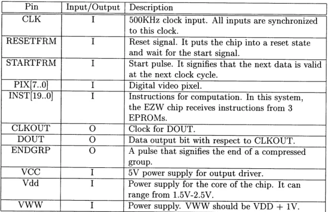
Despite the complexity of the integrated circuit itself, its input and output in-terface is considerably simple to build a system around. Table 2.2 shows the pin descriptions of the chip. In addition to the input and output pins described in the Table, the EZW chips also have many other debugging pins which are not used in this demonstration system.
RESET
START
EZW CLK IN
wait I
a few cycles
EZW DATA IN Pixel 0 Pixel I Pixel 2
(8 bit bus)
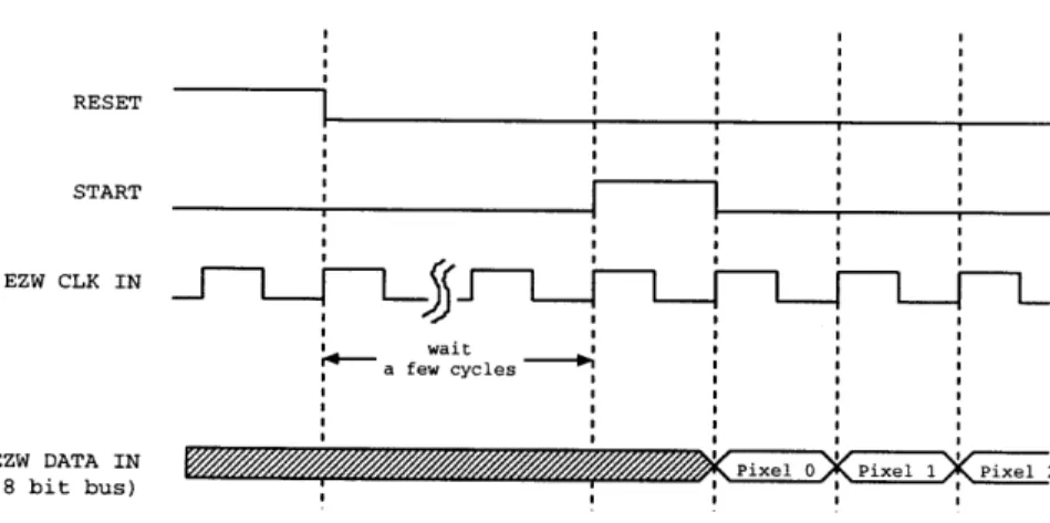
Figure 2-10: Timing Diagram of Input Signals to Video Compression Integrated Circuit
The input interface of this chip is very simple. Figure 2-10 shows the timing dia-gram of input signals to the video compression integrated circuit. When the chip is powered up, it has to be reset before any computation is performed. All input signals are synchronized to EZW CLK IN clock signal which is fixed at 500KHz. The reset
Pin Input/Output Description
CLK I 500KHz clock input. All inputs are synchronized to this clock.
RESETFRM I Reset signal. It puts the chip into a reset state and wait for the start signal.
STARTFRM I Start pulse. It signifies that the next data is valid
at the next clock cycle.
PIX[7..0] I Digital video pixel.
INST[19..0] I Instructions for computation. In this system, the EZW chip receives instructions from 3 EPROMs.
CLKOUT 0 Clock for DOUT.
DOUT 0 Data output bit with respect to CLKOUT.
ENDGRP 0 A pulse that signifies the end of a compressed group.
VCC I 5V power supply for output driver.
Vdd I Power supply for the core of the chip. It can
range from 1.5V-2.5V.
VWW I Power supply. VWW should be VDD + 1V. Table 2.2: Pin descriptions of the EZW chip
EZW DATA OUT X EZW DATA OUT CLK
EZW GROUP CLK
Figure 2-11: Timing Diagram of Output Signals from Video Compression Integrated Circuit
signal, RESETFRM, has to be at least 1 clock cycle. After the chip is reset, it waits for the STAR TFRM signal which should be also at least 1 clock cycle. After the
STARTFRM signal is asserted, each pixel is read continuously into the chip at the
next rising edge of the CLK input signal. When all pixels of a frame are completely delivered, the first pixel of the next frame is immediately delivered at the next clock cycle. At 500Khz, the chip can process 500x103/(128x128) = 30.518 frames per sec-ond.
The output interface, Figure 2-11, of the EZW chip is even simpler than the input interface. There are only 3 output pins from the chip, as described in Table 2.2. The
DOUT is the output data bit and should be read at the rising edge of the CLKOUT
signal. The ENDGRP determines the end of 16 frame group. The chip can assert
CLKOUT sparingly or in bursts depending on spatial and temporal content of the
input frames.
As described previously, the rate of the output bits depends on the voltage level of Vdd. The period of the EZW DAT CLK increases when the Vdd decreases. At the lowest Vdd of 1.5V, the EZW DAT CLK has the longest period of 200 ns. The period of the EZW DAT CLK decreases to 90 ns when Vdd is at its highest value of 2.5V.
This EZW video compression chip requires only a small controller. It needs a reset signal and a start signal which are provided by the Input Frame Buffer module.
+1
D[6. .0]
64MHz 7 bit register
Q[6..01
Q[6] 500KHz clock
Figure 2-12: 64MHz to 500KHz clock divider
The 500KHz clock is generated by dividing the 64MHz system clock by 128 as shown in Figure 2-12. To save some circuit board space, the clock divider is implemented on a CPLD.
2.5
EZW Output Frame Buffer
The EZW Output Frame Buffer basically buffers the output from the video compres-sion chip before it is sent to a PC. Similar to the Input Frame Buffer, the Output Frame Buffer is comprised of SRAM chips and control logic implemented on a CPLD. The EZW Output Frame Buffer receives serial data output from the video chip and writes it to one part of the memory buffer, while at the same time, another part of the buffer is being read to the PC. In other words, this buffer is essentially a ping-pong buffer.
Unlike the Input Buffer described in the previous section, the size of the buffer needs to be estimated. Since the number of bits from the video compression chip can be varied, the capacity of the buffer has to be large enough to hold all the output bits
WRITE
DATA 16 ADDR oloone.
EZW ATAOLEBIT s DATA
EZW DATA CLK 10PACKNG
CS OEWE EZW GROUP CLK - - FSM Write Finish OK x0 Read Finish READ
Parallel Port Interface
Module DATA CS,OE,WE READ/WRITE BUFFER SWITCH 8DATA 1Mb SRAM #0 (8bit wide) ik1 ADDR. 8 J Mb SRAM #1 -q-7--- p 1(8bit wide) CEDOE, WEj
Figure 2-13: Schematic Diagram of the Output Frame Buffer Controller
The video chip compresses a group of 16 or 24 frames.
Each frame has 128 x 128 x 8 or 2(7+7+3 bits.
Therefore, uncompressed 16 frames should have 221 = 2M bits.
For both read and write buffers, the SRAM should have 4M bits of capacity.
However, a dual port SRAM with 4M bits of capacity is not easy to find. In fact, the estimation done above is too conservative. Practically, the video compression has compression ratio of about 100:1 or more, and even in the worst case, the ratio is certainly greater than 2:1, thus reducing the capacity requirement by at least a half. Nonetheless, even 2M-bit dual port SRAMs are still rare. To get around with this problem, a simpler buffer structure is designed. Since 1Mx8 bit SRAMs are commer-cially available from IDT, the buffer is, then, separated into 2 chips of SRAM with another controller implemented on a Cypress CPLD. The final design of the EZW Output Frame Buffer is shown in Figure 2-13. Furthermore, choosing 8bit wide dat-apath also simplifies the system greatly because the parallel port datdat-apath is 8 bits as well.
In Figure 2-13, there are three additional control modules worth discussing here: Bit Packing FSM, Synchronizer FSM, and Read/Write Buffer Switch. Similar to all
o"",
orr
...
tre
...
pw
eve me.. osifb
EZW DAT CLK=O or EZW GRP CLK=O EZW CLK = 1 EZW DAT CLK=1, i !=7
C RESET WAIT FOR ONE Wri et
titionI , WAIT FOR ZERO
Set Addr 0 EZW DATA CLK =1 EZW CLK =0
AVd1
WTFREZW GRP CLK= DAT EZW CLK=1
THO WYGOPEZW GRP CLK= O
WIT LAST BYK
Assertser sga WEE
EZ FO GRP CLK= ZW DAT EZW CLK=1
Aser sin GR L EW RPCL=
Figure 2-14: Bit Packing Finite State Machine
other parts of the system, these three modules are implemented on a CPLD for design flexibility and ease of debugging.
2.5.1
Bit Packing Finite State Machine
As described earlier in the previous section, the output from the video compression chip is serial. However, the data path of this system is 8 bits wide. Implemented on a Cypress CPLD, this Bit Packing Finite State Machine essentially packs 8 bits
together to form a byte and pulses a WE signal to write the bits to a buffer.
Figure 2-14 shows how the finite state machine functions. Although the state diagram looks complicated, the conceptual idea of the machine is very easy. Basically the machine waits for output data from the video chip and writes to the buffer. The
1 bit EZW DATA OUT 0 X C *
EZW DATA OUT CLK 000
MSB 0 1 1 X X X LSB
7 6 5 4 3 2 1 0
1 BYTE BUFFER
Figure 2-15: Bit Storage Format
machine starts from the RESET state, then moves directly to the WAIT FOR ONE state in order to wait for data. When the EZW DAT CLK=1, a signal which means that the EZW DAT BIT holds a valid bit, the machine grabs that bit and writes it to a temporary buffer, as shown in Figure 2-15. From Figure 2-15, the machine writes that bit to the most significant slot available. The following incoming bits are written to the next slot on the right. When the temporary space is full, a condition which means all 8 bits have been stored, the machine asserts a WE signal to the Read/Write Buffer Switch and clears the temporary space. If the temporary space is not full, it simply stores that new bit. The machine then waits for EZW DAT CLK to become 0 in the state WAIT FOR ZERO. The process repeats all over again until
EZW GRP CLK=1. When EZW GRP CLK=1 or all the bits have been received
from the EZW video chip, the machine asserts the WE signal to write whatever it has to the buffer, and the machine notifies Read/Write Buffer Switch by asserting a READY signal. The machine then waits for the OK signal from the Read/Write Buffer Switch module in the WAIT FOR OK state. The assertion of the OK signal, which is done only after both Parallel Port Interface and Bit Packing FSM have fin-ished transmitting and storing bits respectively, means that the Read/Write Buffer Switch has swapped the read and write buffer. Only after the OK signal is received, the Bit Packing FSM can begin capturing output bits again. In some cases, a new bit can arrive from the EZW video chip while the machine is waiting for the OK signal. This situation occurs because the EZW video chip operates independently from the
1 bit EZW DATA OUT 10
EZW DATA OUT CLK
MSB x x 1 XX 1 1 T LSB
7 6 5 4 3 2 1 0
1 BYTE BUFFER
Figure 2-16: An alternative of how to store a bit
EZW Output Frame Buffer. In such a case, the machine simply throws all the bits away in the THROW AWAY GROUP state.
Since the Bit Packing FSM captures bits by sampling EZW DAT CLK, the clock that drives the FSM must be fast enough so that the FSM does not lose any data. From the finite state machine diagram in Figure 2-14, the longest loop between 2 consecutive incoming bits is when the machine traverses the following states in order:
WAIT FOR ONE, WRITE SRAM, and WAIT FOR ZERO. This means that the
clock that drives this state machine has to be fast enough to finish writing a byte to the SRAM while the EZW DAT CLK still maintains its value, otherwise the system would lose 1 bit of information. At the maximum Vdd of the video compression chip, Vdd = 2.5V, the EZW DAT CLK yields the shortest positive pulse, which is 90 ns. So, to guarantee that the system captures all the bits, this FSM has to traverse at least 3 states within 90 ns. Because 64MHz corresponds to 5.76 cycles within 90 ns, this clock frequency was chosen for this FSM. In addition, 64M is conveniently multiple of 2, and it can be divided to generate other clock speed easily.
An alternative to implementing this finite state machine is to write the incoming bit to the least significant bit instead of the most significant bit in an 8 bit temporary space, Figure 2-16. However, this alternative would increase the complexity of the
WAIT FOR DONE
WRITE FINISH = 1 WRITE FINISH = 0 READ FINISH = 1
READ FINISH = 0 Set toggle = !toggle
WAIT FOR CLEARl A t O ig
Figure 2-17: State diagram of parts of Read/Write Buffer Switch
bits that are in the same order as the output bits from the video compression chip. Therefore, if the least significant bit was written first, the software would have to reverse the order of bits every time it received a byte of data from a parallel port.
2.5.2
Synchronizer Finite State Machine
As the name suggests, this finite state machine synchronizes the Bit Packing FSM and the Parallel Port Interface module so that they start their processes at the same time. It ensures that the read buffer has completely been read and that the write buffer has completely been written before they are swapped. Figure 2-17 shows the state transition diagram of this FSM.
This machine simply consists of two states, the WAIT FOR DONE and the WAIT
FOR CLEAR states. The machine waits for a finish signal from both Bit Packing
FSM and Parallel Port Interface in the WAIT FOR DONE state. When both of them send the finish signals to the Synchronizer(not necessarily at the same time), it proceeds to the WAIT FOR CLEAR state. In this state, the machine sends a swap signal to the Read/Write Buffer Switch and simultaneously sends back an OK to the two circuit modules to signify that the read and write buffers have been swapped. The machine goes back to the WAIT FOR DONE state when the two circuit modules
de-assert their finish signals.
2.5.3
Read/Write Buffer Switch
Implemented on a CPLD, this circuit module is basically a switch whose function is to alternate the roles between the read and write SRAM buffers upon receiving a toggle signal from Synchronizer FSM. The swapping process is nothing but re-routing signals as shown in Figure 2-18.
From the schematic diagram in Figure 2-18, the circuit utilizes tri-state buffers to route the signals to their appropriate destinations. The tri-state buffers are con-trolled by the TOGGLE signal sent from the Synchronizer FSM. The roles of the buffer 1 and 0 alternate in accord with the TOGGLE signal. In other words, when
the TOGGLE = 1, the buffer 1 and 0 are write and read buffers, respectively, and vice versa.
2.6
Parallel Port Interface
Implemented in a Cypress CPLD, this circuit module is the connection between the demonstration system and the computer. The main function of this module is to transmit data from the EZW Output Frame Buffer to the PC via parallel port. Al-though the parallel port is normally used to transfer data from a PC to a peripheral, in this demonstration system, it can transmit data from the board to the PC by oper-ating in ECP mode. The protocol to transfer data is simply a hand-shaking protocol shown in Figure 2-19.
Here are the steps to transfer data from the board to a PC:
TOGGLE (from Synchronizer FSM) WRITE ADDRESS[15..0] WRITE DATA[7..0] WRITE CS,OE,WE READ ADDRESS(15. .0) READ DATA[7..0] READ CS,OE,WE
1:
A
______I..
r-r-i
0u > 0 *a 0 SRAM SRAM BUFFER 0 BUFFER 1Figure 2-18: Schematic Diagram of parts of Read/Write Buffer Switch
DO-D7 (bidirectional) PeriphAck(board to PC) Ack(board to PC) HostAck(PC to board) HostCLK(PC to board) ReverseReq(PC to board) AckReverseReq(board to PC)
Figure 2-19: Timing Diagram of the Parallel Port Protocol in ECP mode.
2. When the PC is ready to transmit the data, it brings HostClk high and HostAck low.
3. After a delay of at least 0.5 ms, the PC pulls ReverseReq low to request for incoming data.
4. The board acknowledges by bringing AckReverseReq low.
5. The parallel port can send either "data" or "command" depending on the
Pe-riphAck signal. The difference between a "data" byte and a "command" byte
is that the byte is written into a different memory space on a PC. PeriphAck is high for transmitting "data", and low for "command". Because this demon-stration board always sends data, PeriphAck is always high.
6. The boards brings Ack low to notify the PC that the data is ready to be read. At this point the data bus DO-D7 must hold valid value.
7. The PC acknowledges that it has read the data by pulling HostAck high.
8. The board confirms that the PC has accepted the data by bringing Ack high.
Pin: Signal Function Source Register Pin:
D-SUB Name Centronics
1 HostClk Strobe DO-D7 PC Control 1
2 DO Data Bit 0 PC Data 2
3 D1 Data Bit I PC Data 3
4 D2 Data Bit 2 PC Data 4
5 D3 Data Bit 3 PC Data 5
6 D4 Data Bit 4 PC Data 6
7 D5 Data Bit 5 PC Data 7
8 D6 Data Bit 6 PC Data 8
9 D7 Data Bit 7 PC Data 9
10 Ack Acknowledge Printer Status 10
11 PeriphAck Printer Busy Printer Status 11 12 AckReverseReq Out of Paper Printer Status 12
13 Select Printer Online Printer Status 13
14 HostAck Automatic Line Feed PC Control 14
15 Error Error Printer Status 32
16 ReverseReq Initialize Printer PC Control 31
17 P1284 Select Printer PC Control 36
18-25 Gnd Ground 19-30
Table 2.3: Mapping Between Centronics pinouts and D-SUB pinouts
10. The process repeats starting from step 5 until all the bytes are transfered. Since this demonstration system only sends data to the PC, the ReverseReq is always low.
The state diagram of the finite state machine that controls this transfer process is illustrated in Figure 2-20. While maintaining a hand-shaking process with the PC, the machine reads from the read buffer of the EZW Output Frame Buffer. Since the maximum size of each DMA transfer is 32K bytes, the data has to be divided into 4 blocks of 32K bytes so the total number of transfered bits is IM bits.
This demonstration system uses a 35-pin Centronics(IEEE 1284-B) connector be-cause it is easy to wire and compatible with many other type of connectors. Usually, a standard PC uses a 25-pin D-SUB(IEEE 1284-A) receptacle, the Parallel Port
Inter-else
WAIT FOR REQ .P REVERSE REQ = 0 and
HOST ACK =
SEND DATA
ACK = 0
HOST ACK = 0 I
WAIT FOR HSTACK UP
HOST ACK = 1
WAIT FOR HOSTACK DOWN
ACK 1 HOST ACK = 0 UPDATE ADDR else ONE ONE BYTE
read addr = 2^15(32K)
nReverseReq = 0 WAIT FOR NEXT DMA else
read adr = 2^17(lM)
else WAIT FOR OK OK = 1
read finish=l
Figure 2-20: State diagram of finite state machine that controls the parallel port interface
Cypress CPL
Bt829A REST Bt829A Control Logic
Input Frame Buffer Controller
I 1-- Image EPROM
EZW Controller and Clock Divider
EZW
video Compression
Chip
Figure 2-21: Logic blocks in the first CPLD
face Module has to map Centronics pinouts to D-SUB pinouts using information from Table 2.3. This table is originally for a printer pinout mapping, but this mapping is compatible with this demonstration system as well.
2.7
Complex Programmable Logic Devices(CPLD)
The programmable capability of the Complex Programmable Logic Device(CPLD) allows flexibility of design and ease of implementation and debugging. As mentioned throughout several sections discussed before, most of the logic blocks are implemented on a CPLD. These logic blocks are usually control logic modules, finite state machines, or other complicated logic blocks. The CPLD used in this system is Ultra 37256 man-ufactured by Cypress Semiconductor. The device has 16 logic blocks, each with 16 macrocells, for a total of 256 macrocells. The code is written in VHDL, which is com-piled by Galaxy VHDL compiler and then programmed to the device by Cypress's ISR programming software tool. The VHDL code is simulated using Cypress's Warp VHDL simulation to ensure the functionality and timing property of the generated logic. In addition, each Cypress CPLD can be re-programmed on-board via a JTAG connector. This on-board re-programmable capability simplifies the debugging pro-cess tremendously.
Cypress CPLD Data From____________
EZW Video Compression
Chip Bit Packing FSM
-SRAM BUFFER
RESET Synchronizer Read/Write
AUX FSM Buffer Switch
SRAM BUFFER Parallel Port
TO PC Interface
Figure 2-22: Logic blocks in the second CPLD
Due to the limited size and the I/O pins of a Cypress CPLD, this demonstration system uses 2 of Ultra 37256 Cypress CPLDs. The first CPLD contains logic blocks as shown in Figure 2-21, and the second one is shown in Figure 2-22. All the logic blocks shown in both figures have been discussed in the previous sections. The num-ber of macrocells used in each CPLD is balanced so that both of them still have some space left for debugging and future expansion. In this system, both CPLDs have approximately 60% macrocell utilization.
The only device which can control these two CPLDs are two on-board buttons,
RESET and A UX. The RESET button resets both CPLDs to their default or start
state. The A UX button is an extra button for debugging purposes. The A UX button has proven to be extremely useful for debugging as it was heavily used to generate several test vectors. The ability to use this A UX button would not be possible if the CPLDs were unable to be programmed on-board.
Chapter 3
Software System
This chapter discusses the software part of this demonstration system. The function of the software is to read data from the parallel port, decode the data, and display the decoded image as a movie.
Similar to the hardware system, modularity of the software system helps in de-veloping the software so that it is fast, readable, and easy to debug. The software for this demonstration system is divided into 4 parts: Direct Memory Access(DMA) Device Driver, Decoder, Video Player, and User Interface. The software is built into an executable(.exe) file which can be executed on any Microsoft Windows platform.
User Interface
Data from Data
Furae31lPok aegc Decode Display
3.1
Direct Memory Access Device Driver
This software module is the connection between the hardware and the PC. In order to display the video in real time, the transmission rate from the circuit board to the PC has to be fast enough. For an uncompressed video stream, the rate required is 128x128x8x30 or about 4M bits per second. Given the compression ratio of about 10, the expected data rate for compressed video is approximately 0.4M bps which can be handled by a parallel port in Direct Memory Access(DMA) mode.
In DMA mode, the parallel port controller circuit in a PC bypasses the operating system memory routines and directly accesses the PC's main memory(thus, direct memory access). The DMA mode helps reduce the workload of the processor and increase the speed of data transfer. While the processor is decoding the data, the DMA controller can receive data from the parallel port and then store the data in a memory. The processor only needs to initiate the transfer, after which it can then per-form other tasks while waiting for all the data to be completely stored in the memory.
The DMA device driver used in this demonstration system is WinRT DMA driver from BlueWater Systems Incoperation. BlueWater Systems Inc. provides tool suite to use together with Microsoft Visual C++ compiler to build the software. The driver has two versions: WinRT for Windows 9x and WinRT for Windows NT.
3.2
Decoder
This module takes data from the memory, stored by the WinRT DMA driver, and decodes it into raw images. It is based on a decoder developed by Thomas Simon[4] in C on a Unix platform. The functionality of this decoder is very limited. It can only decode a stream of "0" and "1", which represent bit 0 and bit 1 respectively, and that stream must be in a file with a specific name. The output of this decode is
a series of 128x128 PGM image files. In addition, the original decoder decodes only one group of frames and terminates without freeing memory it has allocated.
Modified for compatibility, the decoder used in this demonstration system is de-signed so that it loops forever and frees all the allocated memory so as to prevent a memory overflow. However, after the modification, the output of the decoder was still not fast enough to keep up with the input from the circuit board. To resolve this difficulty, some frames had to be ignored. So, instead of decoding all 16 images, the decoder decodes only the first few images, stops, discards the rest of the data, and starts with the new group of frames. This solution works well and speeds up the process significantly although the final video output shows some discontinuities.
3.3
Video Player
This module of the software displays the final stream of image frames on the display device. The final image is a 128x128 grey-scale pixel bitmap. To display the images as a movie, the PC simply draws a series of output images one after another. If the software just draws the images one by one, the video will not be smoothly continuous. In fact, if such a drawing algorithm were implemented, one would actually be able to see each pixel being drawn. To prevent such a problem, the image should be first drawn in background and then displayed when it is finished. Figure 3-2 illustrates how using a background page helps smoothen the video play.
As shown in Figure 3-2, there are two copies of memory pages for the video dis-play. The "primary page" is being displayed while the "background page" is being drawn. During the vertical sync, the monitor's electron gun is brought back to the upper left corner. While no image is being drawn on the screen during this vertical sync, the processor can swap the "primary page" and the "background page" point-ers. As a result, every video frame displayed is clear and complete. The video display module of this demonstration system utilizes the Microsoft DirectDraw library which
Pointer to the page being displayed
Pointer to the page in background
Figure 3-2:
Pointer to the page being displayed
The 2 pages are swapped during
vertical sync.
Pointer to the page in background
Double frame buffer
supports such a drawing method.
3.4
User Interface(UI)
The user interface is the layer on top of all the modules. It is a connection between a user and the software which makes the software easily manageable. The UI is written conforming to Microsoft Windows API so that it is compatible with all Microsoft Windows operating systems.
The look and feel of the UI is as shown in Figure 3-3. The UI is composed of 3 Windows components:
1. Radio buttons. These buttons are for users to select the image quality(or com-pression ratio) of the image.
2. Text area. The text area is located at the top left corner of the window. It shows the frame number being displayed and the current compression ratio.