Converter
byRobert C. N. Pilawa-Podgurski
B.S., Massachusetts Institute of Technology (2005)
Submitted to the Department of Electrical Engineering and Computer Science in partial fulfillment of the requirements for the degree of
Master of Engineering at the
MASSACHUSETTS INSTITUTE OF TECHNOLOGY February 2007
c
Massachusetts Institute of Technology MMVII. All rights reserved.
Author . . . . Department of Electrical Engineering and Computer Science
February 2, 2007
Certified by . . . . David J. Perreault Associate Professor, Department of Electrical Engineering and Computer Science Thesis Supervisor
Accepted by . . . . Arthur C. Smith Chairman, Department Committee on Graduate Students
by
Robert C. N. Pilawa-Podgurski
Submitted to the Department of Electrical Engineering and Computer Science on February 2, 2007, in partial fulfillment of the
requirements for the degree of Master of Engineering
Abstract
This thesis presents a resonant boost topology suitable for very high frequency (VHF, 30-300 MHz) dc-dc power conversion. The proposed design is a fixed frequency, fixed duty ratio resonant converter featuring low device stress, high efficiency over a wide load range, and excellent transient performance. A 110 MHz, 23 W experimental converter has been built and evaluated. The input voltage range is 8-16 V (14.4 V nominal), and the selectable output voltage is between 22-34 V (33 V nominal). The converter achieves higher than 87% efficiency at nominal input and output voltages, and maintains efficiency above 80% for loads as small as 5% of full load. Furthermore, efficiency is high over the input and output voltage range.
In addition, a resonant gate drive scheme suitable for VHF operation is presented, which provides rapid startup and low-loss operation. The converter regulates the output using high-bandwidth on-off hysteretic control, which enables fast transient response and efficient light load operation. The low energy storage requirements of the converter allow the use of coreless inductors, thereby eliminating magnetic core loss and introducing the possibility of integration. The target application of the converter is the automotive industry, but the design presented here can be used in a broad range of applications where size, cost, and weight are important, as well as high efficiency and fast transient response.
Thesis Supervisor: David J. Perreault
I want to thank Professor David J. Perreault, my thesis advisor, for all his help and guidance throughout this work. It has truly been a pleasure working with such a knowledgeable and experienced individual. He is an outstanding researcher and educator, and I am grateful to have been given the opportunity to learn from him.
Dr. Juan Rivas provided invaluable assistance and expertise throughout this work, and his willingness to always lend a helping hand is indeed inspiring. Anthony Sagneri provided considerable assistance as well, for which I am very grateful. I would also like to thank the rest of my research group, all of whom I have learned a great deal from: Yehui Han, Olivia Leitermann, Brandon Pierquet, Jackie Hu, and David Giuliano.
To all of my friends and colleagues at LEES, thanks for making it a great place to work. Throughout this process, I have made many new friends here, and I thoroughly enjoy the daily interactions with such a diverse and intelligent group of people.
Vivian Mizuno deserves accolades for all the hard work she puts in to make the laboratory run as smoothly as it does. I am also grateful for all the help she provided in handling all my purchasing orders, or any other problem I had.
Dr. Thomas Keim and Professors James Kirtley, Jr. and Steven Leeb have all contributed to my development as a student and engineer, for which I am grateful.
I would like to thank my parents, Maria and Peter, for their love and for being the best parents one could ask for. Without their support - in whatever my endeavours - I would not be where I am today.
This work was initially sponsored by the MIT/Industry Consortium on Advanced Auto-motive Electrical/Electronic Components and Systems. Additional support was provided by the Siebel Scholars Foundation from whom I received a Siebel Fellowship for the fall semester of 2006. I would also like to take this opportunity to thank the foundation “Erik och G¨oran Ennerfelts Fond f¨or Svensk Ungdoms Internationella Studier”, whose generous financial assistance helped realize my dream of coming to MIT as an undergraduate.
Last but certainly not least, I would like to express my gratitude to my wife Brooke, who has been with me throughout this entire process, providing love and support. Having her by my side has made my task so much more enjoyable. I hope to one day get the opportunity to show her the same patience and understanding that she has shown me while I completed this work.
1 Introduction 19
1.1 Research Background . . . 20
1.2 Thesis Objectives, Contributions, and Organization . . . 22
2 Power Converter Topologies 25 2.1 Hard Switched Converters . . . 25
2.2 Soft Switching Converters . . . 27
2.2.1 Class E Inverter . . . 28
3 Resonant Boost Converter 31 3.1 Inverter Stage . . . 32
3.1.1 Inverter Background . . . 32
3.2 Rectifier Stage . . . 40
3.2.1 Rectifier Design . . . 42
3.3 Simulated Converter Performance . . . 43
3.3.1 Converter Waveforms . . . 43
3.3.2 Simulated Converter Loss Contributions by Components . . . 44
4 Semiconductor Selection and Modeling 47 4.1 Device Selection . . . 47
4.1.1 Vertical Power MOSFETs . . . 48
4.2 Device Characterization . . . 57
4.2.1 Non-linear Output Capacitance . . . 57
4.3 SPICE Modeling . . . . 58
4.3.1 Transistor Model . . . 59
4.3.2 Diode Model . . . 60
5 Resonant Gate Drive Circuit 63 5.1 Resonant Gating Concepts . . . 63
5.1.1 Hard Gating . . . 63
5.1.2 Resonant Gating . . . 65
5.2 Gate Drive Implementation . . . 67
5.2.1 Self-oscillating Feedback Network . . . 69
5.2.2 Simulation of Resonant Gate Drive with Feedback Network . . . 70
5.2.3 Gate Drive Startup . . . 70
6 Control Architecture 75 6.1 General Theory . . . 75
6.1.1 Resonant Converter Control Strategies . . . 75
6.1.2 On-off Control . . . 76
6.2 Example Implementation . . . 78
6.2.1 Reference Voltage . . . 78
6.2.2 Comparator and Hysteresis Band . . . 79
6.2.3 Gate Drive Turn-On . . . 85
6.2.4 Powering the Logic Chips . . . 85
7 Design and Layout 87 7.1 Power Stage . . . 87
7.1.1 Power Stage Board Layout . . . 89
7.1.2 Power Stage Components . . . 90
7.2 Gate Drive Circuit . . . 90
7.3 Control Circuitry . . . 93
8 Experimental Results 97 8.1 Measurement Setup . . . 97
8.2 Converter Waveforms . . . 99
8.2.1 Steady State Waveforms . . . 99
8.2.2 Startup and Shutdown Waveforms . . . 99
8.3 Open-Loop Converter Efficiency . . . 103
8.3.1 Continuous Operation . . . 103
8.3.2 Modulation Frequency . . . 104
8.4 Closed-Loop Converter Efficiency . . . 105
8.5 Output Voltage Ripple . . . 106
8.6 Transient Performance . . . 106
8.6.1 Output Voltage Step . . . 106
8.6.2 Load Step . . . 109
9 Summary and Conclusions 113 9.1 Thesis Summary and Contributions . . . 113
9.2 Future Work . . . 114
A SPICE Code 117 A.1 Φ2 Converter SPICE Code . . . 117
B SPICE Semiconductor Models 123 B.1 SPICE Transistor Model . . . 123 B.2 Non-ideal Diode SPICE Model . . . 124
C PCB Layout 127
D Derivation of Ideal Ratio of Fundamental and Third Harmonic Voltages
for Minimimum Synthesized Voltage 131
E LabVIEWTMInterface 135
1.1 Block diagram illustrating the structure of a very high frequency dc-dc con-verter. . . 20 2.1 Buck Converter - a conventional, hard switched, converter. . . 26 2.2 Drain-to-source voltage and current waveforms during an off-to-on transition
of the buck converter of Figure 2.1. . . 27 2.3 Class E inverter. Cds comprises parasitic device capacitance and possibly
added discrete capacitance. . . 28 3.1 Schematic of resonant boost converter topology, consisting of a Φ2 inverter
coupled with a resonant rectifier. . . 31 3.2 Shorted uniform, lossless transmission line of characteristic impedance Z0. . 32
3.3 (a) Reactance of shorted transmission line. (b) Impedance for shorted quarter-wave transmission line. . . 33 3.4 Schematic drawing of Class Φ inverter. . . 34 3.5 (a) Multiresonant network used to shape drain to source voltage. (b) Impedance
magnitude vs. frequency for network tuned according to Equation 3.6 with CF = 100 pF and fs = 110 MHz. . . 35
3.6 Illustration of synthesized waveforms for different ratios of V3f and Vf. . . . 36
3.7 (a) Schematic of Φ2 structure. (b) Φ2 inverter with load network. . . 38
3.8 (a) Impedance magnitude plot for circuit of Figure 3.7(b). (b) Time do-main simulation showing drain voltage plot for circuit of Figure 3.7(b) with Vin =14.4 V and fs = 110 MHz. . . 39
3.9 (a) Rectifier with dc path from input to output, suitable for boost appli-cations. (b) Rectifier with blocking capacitor, suitable for buck or boost applications. . . 41
3.10 Circuit illustrating one possible model for tuning of the resonant boost rectifier. 42 3.11 Schematic of resonant boost converter topology used for simulated waveforms
of Figure 3.12. . . 43 3.12 Simulated Converter Waveforms. . . 45 3.13 Simulated converter loss breakdown by component. . . 46
4.1 Schematic drawing of power MOSFET with key parasitic element shown as discrete components. . . 48 4.2 Scatter plot of potential 60 V vertical MOSFETs. . . 51 4.3 Plot of normalized power loss vs. frequency for 60 V vertical MOSFETs. . . 52 4.4 Plot of normalized power loss versus output power for the top three vertical
MOSFETs. . . 53 4.5 Plot of measured non-linear output capacitance of MRF6S9060. . . 58 4.6 Schematic drawing of SPICE model which captures the relevant characteristic
of transistors suitable for resonant dc-dc power converters. . . 60 4.7 Implementation of variable resistance of voltage controlled switch between
nodes D and S of Figure 4.6. . . 61 4.8 Schematic drawing of diode SPICE circuit which properly models the
non-linear diode capacitance, as well as the forward voltage drop and package inductance. . . 61 4.9 Plot comparing output capacitance of SPICE model to measured capacitance
of S310 for different reverse voltages. . . 62 5.1 Circuit illustrating hard gating concept. . . 64 5.2 Circuit illustrating resonant gating concept. . . 65 5.3 Plot of gating loss for resonant and hard gating with parameters from the
MRF6S9060 rf MOSFET. Note that the MRF6S9060 cannot, in fact use sinusoidal gating for reasons discussed in the following section. . . 66 5.4 Schematic drawing of a Φ2-based gate drive circuit which provides
5.5 Simulated quasi-square wave gate voltages of Smain(top), when Sauxis driven
with a sinusoidal voltage source (bottom). Component values as listed in table. 68 5.6 Schematic drawing of self-oscillating feedback network which provides 180◦
of phase shift between node A and B for component values as listed in table. 69 5.7 Magnitude (a) and phase (b) of the feedback transfer function VB
VA of Figure 5.6. 70 5.8 Gate drive drain impedance (node A of Figure 5.4) with feedback network
connected and disconnected. . . 71 5.9 Schematic drawing of gate drive circuit with attached feedback network. . . 71 5.10 Simulated waveforms at the gate of Smain (top) and gate of Saux (bottom)
for the circuit of Figure 5.9. . . 72 5.11 Schematic drawing of experimental implementation of the gate drive circuit
with inductor Lstart to improve startup time. . . 73
6.1 A block diagram illustrating on/off control of a VHF resonant dc-dc con-verter. This control strategy enables efficient operation over a wide load range and allows the converter to be optimized for a fixed frequency and duty ratio. . . 77 6.2 A block diagram illustrating the voltage divider network used to measure the
output voltage and compare it to a desired reference voltage. The capacitor C10 and resistor R4 provide high-frequency filtering of the converter output
signal. . . 78 6.3 A schematic of a hysteretic control circuit, complete with voltage divider
network and hysteretic feedback network. Component values for the experi-mental implementation are given in Table 7.3 of Chapter 7. . . 79 6.4 A schematic of a dynamic hysteretic control circuit, which employs a
capaci-tor in the feedback path to mitigate problems associated with high frequency pickup. Component values for the experimental implementation are given in Table 7.3 of Chapter 7. . . 81 6.5 Simulated results for dynamic hysteresis and regular hysteresis. . . 84 6.6 Simulated results for dynamic hysteresis with resistor R3 removed from the
feedback path. . . 85 6.7 Complete schematic of converter control scheme. See Table 7.3 of Chapter 7
7.1 Converter photographs of top and bottom sides with cm ruler shown for scale. 88 7.2 Photograph of converter with the power stage components labelled. . . 88 7.3 Schematic of resonant boost converter. . . 89 7.4 Schematic of resonant boost converter with one critical layout path highlighted. 90 7.5 Photograph of prototype board with gate components labelled. . . 91 7.6 Schematic of gate drive circuit. . . 92 7.7 Photograph of bottom side of prototype board with the control circuit
semi-conductors labelled. . . 93 7.8 Schematic of control circuit with auxiliary components. . . 95 8.1 Block diagram of measurement setup. . . 98 8.2 Drain and gate voltage for experimental 110 MHz converter operating with
Vin = 14.4 V and Vout = 33 V. . . 100
8.3 Waveforms illustrating converter startup. Operating conditions: Vin= 14.4 V,
Vout= 33 V. . . 101
8.4 Waveforms illustrating converter shutdown. Operating conditions: Vin =
14.4 V, Vout= 33 V. . . 102
8.5 Open-loop power and efficiency over the input voltage range, with Vout fixed
at 32 V. . . 103 8.6 Converter open-loop efficiency vs. modulation frequency for 50% duty ratio.
The input voltage is 14.4 V and the output voltage is fixed at 33 V by the electronic load. . . 104 8.7 Converter efficiency over the input voltage range, parametrized by load. The
output voltage is regulated at 32.4 V. . . 105 8.8 Steady state converter waveforms, illustrating output voltage ripple (a),
con-verter command signal (b) and the corresponding drain voltage (c). Vin =
14.4 V, Vout = 32.4 V, Rload = 100 Ω. . . 107
8.9 Output voltage waveform illustrating converter response to a change in reg-ulated voltage. . . 108 8.10 Circuit used to step the converter reference, resulting in a change in output
8.11 Load step circuit for characterizing transient performance of converter. . . . 110
8.12 Converter response to load step. The converter response to a change in load is instantaneous, without any voltage deviation outsides of the steady state ripple range. . . 111
C.1 Converter PCB layout, top side. . . 127
C.2 Converter PCB layout, top copper layer. . . 128
C.3 Converter PCB layout, top silkscreen layer. . . 128
C.4 Converter PCB layout, bottom side (mirrored). . . 129
C.5 Converter PCB layout, bottom side. . . 129
C.6 Converter PCB layout, bottom copper layer. . . 130
C.7 Converter PCB layout, bottom silkscreen layer. . . 130
D.1 Plot of Equation D.2 for various ratios of V3f and Vf. . . 132
D.2 Illustration of synthesized waveforms for different ratios of V3f and Vf. . . . 133
D.3 Illustration of synthesized waveforms for the value V3f/Vf = 1/6 and small deviations above and below this ratio. Minimum voltage is achieved for the ratio 1/6. . . 134
E.1 Software interface for LabVIEWTM, which is used to control the multimeters. The software enables realtime collection and display of converter efficiency and power, as well as input and output voltages and currents. . . 136
3.1 Component loss contributions. . . 46
4.1 Measured device parameters for 60 V vertical MOSFETs . . . 50
4.2 Measured data for top five LDMOS candidates selected for use in prototype resonant boost converter. . . 55
4.3 Resistor values and switch thresholds that provide a piecewise linear resis-tance model to characterize Rds,on of MRF6S9060. . . 61
7.1 Component values for power stage. . . 91
7.2 Component values for gate drive circuit implementation. . . 92
Introduction
P
OWER electronics today are facing increasing demands for miniaturization, improved efficiency, and reduced cost. In dc-dc power conversion a switched topology is often the only way to achieve reasonable efficiency. By using semiconductor switches and energy storage devices that ideally do not dissipate energy, high efficiency can be achieved. The trade-off for high efficiency is in the cost and size of the passive energy storage, which can often-time be the dominant factor for a given topology. In order to reduce the size of the passive components, it is necessary to increase the switching frequency.The incentive to move to higher frequencies is not only given by the reduced sizes of the passive components, but also by transient performance. With smaller capacitors and inductors, less energy is stored in the converter, allowing for a faster response to a change in load. It is thus clear that much can be gained from moving to a design that enables operation at very high frequency
There is, however, a cost to be paid for moving up in frequency. Semiconductor losses increase with frequency, as do magnetic core losses. This is why the fastest conventional dc-dc converters today are switched at frequencies less than 10 MHz. Power converters that operate at above 10 MHz are often resonant topologies, which reduce switching loss and often absorb the semiconductor parasitics. The use of resonant converters for dc-dc power conversion introduces many new challenges in the areas of control, design, modeling, and layout. This thesis presents an approach to overcome those challenges, and through experimental results illustrates the substantial benefits that can be realized once those challenges are overcome.
1.1
Research Background
In conventional, hard-switched, power converters the power loss associated with each switch-ing cycle is what often sets an upper bound on frequency of operation. Durswitch-ing turn-on and turn-off of the semiconductor switches, the currents and voltages cannot change instan-taneously. The resulting current-voltage overlap results in a power loss, which increases linearly with frequency.
One way to maintain high efficiency at high frequency is to employ a low switching-loss converter topology, incorporating Zero-Voltage-Switching (ZVS), or Zero-Current-Switching (ZCS). These techniques are also often referred to as soft switching [1–5]. Resonant con-verters can provide these features by using resonant elements (capacitors and inductors) to control the switch voltage and/or current during on-off transitions. Resonant topologies are frequently used in radio-frequency (rf) amplifiers, and many of the techniques used in that field can also be applied to dc-dc converters [6].
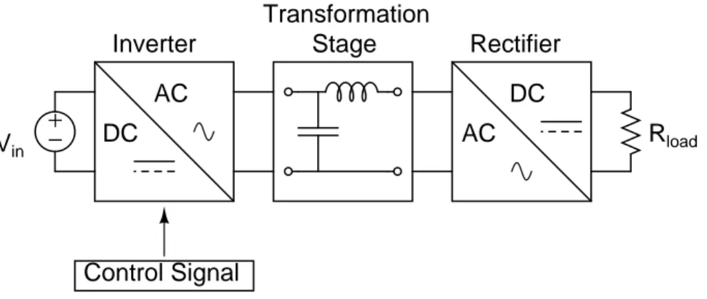
A structural design similar to that of Figure 1.1 is often employed in resonant dc-dc converters [7–12]. At the input stage a resonant inverter converts the input dc voltage to a high frequency ac voltage. A transformation stage then performs the requisite voltage transformation, and a resonant rectifier transforms the ac waveform back to dc. Not explic-itly shown in Figure 1.1 are input and output filters - components that are often required to ensure that the converter meets safety and performance specifications.
AC
DC
AC
DC
+
−
V
inR
loadControl Signal
Inverter
Transformation
Stage
Rectifier
Figure 1.1: Block diagram illustrating the structure of a very high frequency dc-dc converter.
than conventional hard-switched designs, it also introduces some new challenges. One ex-ample is control of the converter, which becomes more difficult as frequency increases. Frequency control is often used to regulate resonant converters. However, this typically yields poor efficiency at light load due to the many loss components that do not scale back with power, and due to the variation in circuit waveforms as frequency is adjusted. Like-wise, another commonly used control strategy - pulse-width modulation, also finds limited used at very high frequency. This is because achieving duty ratio control is difficult (and typically unattractive from a gate drive loss perspective) at high frequencies, and because the performance of many resonant topologies is very sensitive to duty ratio.
In addition to being challenging to control, resonant converters often suffer from poor light load performance, as discussed in [3, 6–8, 10, 13, 14]. In some converters the resonant elements that help achieve ZVS conditions are sized for a specific load impedance. As the load impedance changes, ZVS can no longer be maintained, resulting in increased switching loss and consequently lower efficiency. Other topologies maintain ZVS conditions across the load range, but incur much higher resonant losses at light load due to increased circulating currents in the resonant elements. Because of this characteristic of resonant converters, care must be taken in our design to maintain high efficiency at light load.
One technique that has proven useful to control VHF dc-dc power converters is on-off control [12, 15, 16], also known as cell-modulation control [12, 16] or burst-mode control. In the simplest version of this approach, an rf converter cell is optimized for a narrow load range and fixed frequency and duty ratio. To control power, the entire cell is modulated on and off (bang-bang control) such that the average power delivered to the output is as needed to regulate the output voltage. Moreover, this strategy can be extended for use with multiple converter cells [12]. As the load varies, the number of cells in use is changed, allowing for efficient operation over a wide load range. This approach allows the benefits of resonant converters to be realized (high efficiency at very high frequency) while maintaining high efficiency at light load. It is important to realize that the passive elements of the converter can be made very small, as they are sized by the rf switching frequency. In addition to reducing the converter size, this approach greatly improves the transient performance, since very little energy is stored in the passives in each switching cycle. The only passive component that needs to be sized based on the modulation frequency (the frequency at which the converter cell is modulated on and off) is the output filter capacitor.
The benefits in terms of size, cost, and transient performance makes the cell-modulated architecture an attractive option.
1.2
Thesis Objectives, Contributions, and Organization
The goal of this thesis is to design and build a very high frequency (VHF, 30-300 MHz) dc-dc converter with the following specifications:
• Input Voltage: 8-16 V
• Output Voltage (selectable): 22-34 V • Switching Frequency: 110 MHz • Output Power Rating: 15-25 W
As Chapter 2 will illustrate, conventional power converters cannot operate at the high frequency desired while maintaining acceptable efficiency. Section 2.2 describes the common solution for high frequency dc-dc power conversion - resonant topologies. In addition to providing background and discussion of previous work, it also highlights some limitations and undesirable characteristics of conventional resonant converters.
In Chapter 3, a resonant boost topology suitable for VHF operation is introduced which overcomes many of the limitations outlined in Section 2.2. The design features a fixed frequency, fixed duty ratio highly efficient inverter stage coupled with a resonant rectifier. Detailed design procedures are presented for the inverter and rectifier stages in Sections 3.1 and 3.2, respectively.
To achieve high performance and efficiency, much care must be taken in the choice and modeling of the the main semiconductor switch. A detailed analysis of the essential parame-ters governing semiconductor loss is presented in Chapter 4, as well as semiconductor SPICE models appropriate for simulation of the complete converter. The chapter also presents a qualitative comparison between a number of possible high performance rf MOSFETs for use in VHF dc-dc power converters.
Chapter 5 introduces a low-loss resonant gate drive scheme suitable for VHF operation. This approach, which is closely related to that introduced in [16], provides rapid startup and shutdown as well as low parts count. The converter utilizes a high bandwidth hysteretic controller for on-off control, providing fast transient response and good efficiency over a wide load range. The details of the control scheme are presented in Chapter 6.
Chapter 7 discusses design and layout considerations for VHF dc-dc converters. The chapter also provides component values for the Φ2-based power stage, resonant gate drive
circuit, and the on/off control circuitry of an experimental prototype. In addition, pho-tographs with labelled components are presented along with schematics illustrating critical loops from a layout perspective.
Chapter 8 provides experimental measurements and evaluations of the converter. Impor-tant characteristics such as efficiency, power, output voltage ripple and transient perfor-mance are evaluated for different operating points.
Finally, Chapter 9 concludes the thesis with a summary of the contributions of this work and a discussion of possible future research directions.
Power Converter Topologies
I
N the quest for higher power densities the trend in power electronics has been to oper-ate at higher frequencies. Typically, power converters operoper-ate at the highest frequency possible for a given efficiency specification. One loss mechanism that typically limits the op-erating frequency of conventional dc-dc converters is switching loss, which increases linearly with frequency. Much work [1–5] has therefore focused on new topologies that mitigate the switching loss, thereby allowing an increase in switching frequency. The following section will briefly discuss hard switched converters and their limitations, followed by a treatment of resonant soft-switched converters. The chapter will conclude with a survey of a subset of resonant topologies suitable for dc-dc power conversion, along with a discussion of their respective restrictions.2.1
Hard Switched Converters
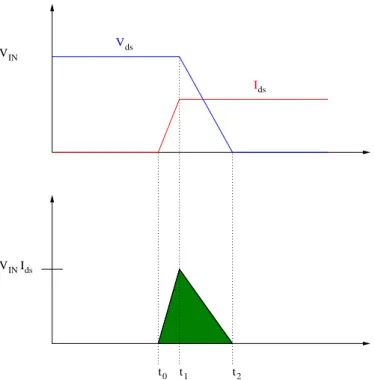
There are many different topologies of hard switched dc-dc converters, but their switching loss mechanisms are similar. The concept of switching loss will here be illustrated by the classic buck converter, shown in Figure 2.1 [17]. The subsequent switching loss discussion makes many simplifying assumptions such as that of linear parasitic capacitors, which is certainly not the case in real devices. This analysis only aims to illustrate the concept of switching loss, not to give a full derivation of all subtleties involved in this loss mechanisms. For a more thorough discussion of switching loss, please refer to [?].
Figure 2.2 shows the drain-to-source voltage and current during the MOSFET’s off-to-on transition. In this example, the diode is assumed to be ideal. Initially, the MOSFET is turned off, and the diode is carrying all of the load current, Io. Before the diode can turn
+
−
L
oC
oD
R
loadV
in+
V
ds-I
dsI
oFigure 2.1: Buck Converter - a conventional, hard switched, converter.
as the time between t0 and t1. During this time the MOSFET supports both a high voltage
and a high current, which results in a power loss. At time t1 the diode becomes reverse
biased and turns off, allowing the drain-to-source voltage Vdsto fall to 0. The instantaneous
power dissipated in the MOSFET is given by the product VdsIds, and is shown as the shaded
triangle in the lower graph of Figure 2.2. Assuming piecewise linear waveforms, the energy lost during each turn-on transition is then simply given by:
Won=
1
2VdsIds(t2− t0) (2.1)
The transition times t0 through t2 are not instantaneous because of the parasitic
capac-itances associated with the MOSFET, and the charging and discharging of these take a finite amount of time. The parasitics of the MOSFET will be discussed further in Chap-ter 4. In the case of the turn-on transition, there is one additional loss mechanism. The energy stored in the parasitic drain-to-source capacitor is dissipated through the MOSFET to ground, resulting in an energy loss of 12CV2 (for the simplifying case of linear capacitor, which is an idealization). The energy lost in the turn-off transition, Wof f, is similar to
the one described by Equation 2.1, resulting in a total energy loss per switching cycle of Wsw = Wof f + Won. Since this happens once every switching cycle, this power loss clearly
increases linearly with frequency. Although the energy lost in each cycle is relatively small, the resulting switching loss can cause a significant drop in converter efficiency as we move to high frequencies.
Vds
Ids
VIN
VINIds
t0 t1 t2
Figure 2.2: Drain-to-source voltage and current waveforms during an off-to-on transition of the buck converter of Figure 2.1.
2.2
Soft Switching Converters
In order to reduce switching loss, it is desirable to control the voltage and/or current to eliminate the overlap illustrated in Figure 2.2. By ensuring that the on/off transitions of the semiconductor devices occur at time when the waveform of interest (voltage or current) is zero, soft switching can be achieved. Resonant converters typically achieve this by us-ing reactive networks to significantly reduce the semiconductor current or voltage durus-ing switching. Many types of soft switching converters exist [1–5], and they can be classified as zero-voltage switching (ZVS), zero-current switching (ZCS), or both. All have in common that they reduce the switching loss experienced in hard switched converters. Many of them also have the added advantage of absorbing the parasitics as part of their resonant network, and to recover the energy stored in the parasitics. If the switching frequency is sufficiently high, some discrete components of the resonant network can be completely replaced by the parasitics. Although this requires tighter control of the semiconductor parasitics than is found in conventional converters, it is nevertheless a powerful idea: exploiting the parasitics
to achieve higher performance and power density
A typical penalty for reducing switching loss in resonant soft-switched converters is the higher device stresses [2, 3, 6–10, 13, 14, 16, 18, 19], as well as higher conduction losses. Fur-thermore, as can be seen in [3, 6–8, 10, 13, 14], it is often difficult to maintain high efficiency over a wide load range with resonant converters. As a practical illustration the following section will examine some of these limitations seen in the Class E inverter [20], which is a common resonant topology used in dc-dc power converters [?, 7, 10, 12, 13]. Other resonant topologies exhibit similar characteristics.
2.2.1 Class E Inverter
The Class E inverter, depicted in Figure 2.3, is a highly efficient resonant topology often used in rf power amplifiers. Its successful use in resonant dc-dc power converters is also well known [6, 7, 9, 12].
+
−
V
inL
chokeL
RC
RC
dsR
L+
-V
out +-v
dsFigure 2.3: Class E inverter. Cdscomprises parasitic device capacitance and possibly added discrete
capacitance.
The input inductor Lchokeis large enough so that the current through it can be considered
constant and inductor approximates an open circuit at radio frequencies. The resonant tank (LR, CR, RL) is tuned in conjunction with Cds to provide a switching waveform with zero
voltage and zero time-derivative of voltage at turn-on. Furthermore, the switch voltage rise at turn-off is delayed until the current has decreased to zero. These conditions, which reduce switching loss by time-displacement of switch voltage and current, are known as Class E switching conditions.
inverter are certain undesirable characteristics that limit miniaturization and performance:
• The RF choke inductor Lchoke is relatively large, limiting transient performance and
miniaturization.
• Voltage device stresses are high (Vdspeak ≥ 3.6 Vin), requiring the use of less efficient semiconductors.
• Output power is tightly dependent on Cds.
Topologies that address some of these issues have been developed, such as the ‘Even Harmonic Resonant Class E’ [21, 22], which reduced the size of the RF choke inductor. Others, such as the Class F inverter [23,24] use harmonic frequency resonators to shape the drain waveform to reduce device voltage stress. However, practical implementation of these types of inverters exhibit significant overlap of drain-to-source voltage and current (i.e., do not operate in “switched-mode”), thus decreasing efficiency, making them unsuitable for dc-dc converter applications.
Inverters that both reduce device stress and energy storage requirements are presented in [25,26] (termed Class Φ for their relation to the traditional Class F). However, the proposed solutions employ high-order resonant structures requiring many passive components, which may not be realizable in all applications.
As this chapter has illustrated, resonant converters provide good efficiency for very high operating frequency due to reduction of switching loss. There is, however, a need for resonant topologies that provide reduced switch stress - enabling the use of more efficient semiconductor switches with lower device breakdown. Furthermore, in order to achieve miniaturization, and possibly integration, resonant topologies that employ small-valued passive components are highly desirable.
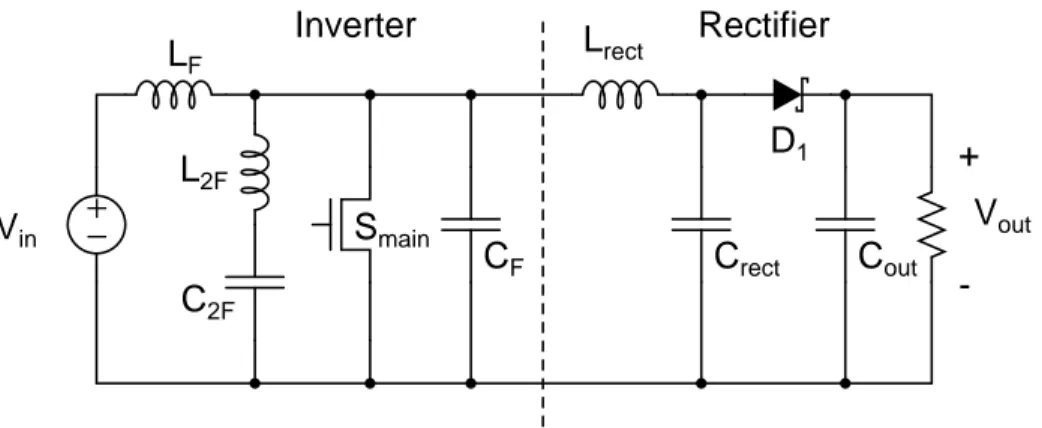
Resonant Boost Converter
T
HE limiting properties of existing resonant topologies highlighted in Chapter 2 mo-tivates the investigation of new topologies better suited for dc-dc power conversion. This chapter introduces a new resonant boost topology that has been developed specifically to address some of the shortcomings of earlier solutions. The converter, shown in Figure 3.1 can be viewed as a special version of the Class Φ inverter, described in [25–29], coupled with a resonant rectifier. The design was developed with on-off control in mind (explained in detail in Chapter 6) and can therefore be optimized for low device stress and high effi-ciency at a fixed frequency and duty ratio. This enables the use of low-loss resonant gating which together with zero-voltage switching provides efficient operation in the VHF region. Section 3.1 explains the operation and design of the inverter stage, followed by details of the rectifier design and its coupling to the inverter stage in Section 3.2. Section 3.3 con-cludes the chapter with simulated converter waveforms and converter loss breakdown by component.+
−
V
in+
-V
outL
FL
2FC
2FC
FC
rectL
rectC
outD
1Inverter
Rectifier
S
mainFigure 3.1: Schematic of resonant boost converter topology, consisting of a Φ2 inverter coupled
3.1
Inverter Stage
3.1.1 Inverter Background
Wave-shaping Network Theory
For a transmission line of length l, characteristic impedance Z0 =
q
L
C, where L and C are
distributed inductance and capacitance (per unit length), the input impedance Zin is given
by [30]:
Zin = Z0
ZLcos kl + Z0j sin kl
Z0cos kl + ZLj sin kl
(3.1) where k = 2πλ is known as the wave number. For the case where the end of the transmission line is shorted (depicted in Figure 3.2), Equation 3.1 becomes:
Zin= Z0j tan kl (3.2) Z0 = q L C Zin l Z0
Figure 3.2: Shorted uniform, lossless transmission line of characteristic impedance Z0.
Figure 3.3(a) illustrates the reactance of a shorted 75 Ω transmission line. For the case when the length l of the transmission line is equal to one quarter wavelength (λ/4), it can be seen that the input impedance Zin has poles for frequencies:
f = n
4l√LC for n = 1,3,5,... (3.3)
Similarly, Zin has zeros for even n (0,2,4...). Consequently, for an exciting waveform of
frequency fs, the shorted quarter-wave transmission line presents high impedance (peaks)
at all odd harmonics, and low impedance (nulls) at all even harmonics. This is shown by the impedance magnitude plot of Figure 3.3(b). For this plot, the length l corresponds to
λ/4 for the frequency 110 MHz, and Z0 = 75 Ω. A similar analysis of a transmission line
terminated by an open circuit gives the complementary result: impedance peaks at dc and even harmonics, and nulls at odd harmonics of the switching frequency.
0 −400 −300 −200 −100 0 100 200 300 400
Reactance for Short Circuit 75Ω Transmission Line
π/2 π 3π/2 2π 5π/2 3π kl Z0 ta n k l
(a) Reactance of shorted 75 Ω transmission line.
110 220 330 440 550 660 770 880 990 −10 0 10 20 30 40 50 60 70 80 Frequency [MHz] Impedance [dB Ω ]
Impedance vs. Frequency for Shorted Quarter Wave Transmission Line
(b) Impedance plot for shorted 75 Ω quarter-wave transmission line of Figure 3.2 with l = λ/4 for fs = 110 MHz.
Figure 3.3: (a) Reactance of shorted transmission line. (b) Impedance for shorted quarter-wave transmission line.
These aligned peaks and nulls constrain the waveforms that can be supported by the transmission line. The impedance of the shorted quarter-wave transmission line is shown in Figure 3.3(b), and will not support voltages of even harmonics when driven by an excitation of frequency fs. Consequently, the signal will only contain odd harmonics and will therefore
be half-wave symmetric [31].
These characteristics of transmission lines and their lumped element counterparts -have been used to reduce switch stress in rf power amplifiers by shaping the drain-to-source waveform [23–29, 32–36].
As is shown in [25–27], these symmetrizing properties of a quarter-wave transmission line can be used to shape the drain-to-source voltage in a resonant switching converter topology. In particular, [27] gives a detailed description of the operating principle of the Class Φ inverter, depicted in Figure 3.4. This inverter operates fully in “switched-mode”, at duty ratios somewhat less than 50%.
However, a transmission line presents practical difficulties for implementation in a VHF power converter. The added size and cost of a quarter-wave transmission line can negate
+ − Vin LR CR Cds RL + -Vout + -vds
quarter-wave transmission line
Figure 3.4: Schematic drawing of Class Φ inverter.
much of the benefits of switching at a high frequency, making it a less attractive solution. An alternative is the lumped transmission line analogs of [25–27], which use tapped inductors to create multi-resonant structures with symmetrizing properties similar to those of the quarter-wave transmission line. While their successful construction and implementation have been experimentally demonstrated, their fabrication requires substantial effort.
In an effort to utilize the waveshaping properties of the quarter-wave transmission line, the multi-resonant network of Figure 3.5(a) can be employed to provide a low-order approx-imation of the networks developed in [26]. As is seen in Figure 3.5(b), for a certain selection of components [28], the resulting input impedance mimics that of the shorted transmission line (Figure 3.3(b)) for the fundamental, second, and third harmonic of the switching fre-quency1. The resonant elements C
F, C2F, LF, and L2F can be made small, and as outlined
in [27], can replace large bulk elements of similar topologies. Furthermore, the component CF can comprise parasitic switch capacitance (and optional added discrete capacitance),
providing parasitic absorption. Another benefit of the low-order multiresonant network is the low parts count that it offers, compared to a high-order network that attempts to more closely approximate the quarter-wave transmission line impedance at yet higher harmonics. Fewer components translates to reduced size, weight, and cost, which is always desirable. Because of these advantages, the multi-resonant network of Figure 3.5(a) is employed in the topology developed for this work.
1
Note that appropriate selections of passive component values for optimum converter operation do not typically load the network having the exact impedance peaks of a quarter-wave line, though the zero is typically selected close to the second harmonic. This will be treated subsequently.
L
FL
2FC
2FC
FZ
in(a) Multiresonant network.
0 110 220 330 440 −40 −20 0 20 40 60 80 Frequency [MHz] Impedance [dB Ω ] Z
IN vs. Frequency for Multi Resonant Network
(b) Impedance Plot of Zin.
Figure 3.5: (a) Multiresonant network used to shape drain to source voltage. (b) Impedance mag-nitude vs. frequency for network tuned according to Equation 3.6 with CF = 100 pF and fs = 110
MHz.
Multi-resonant Network Implementation
By carefully controlling the impedances at a finite number of harmonics of the switching frequency, the drain-to-source voltage of a converter can be shaped to reduce overall switch voltage stress. Such a flattening of converter waveforms is widely used in Class F rf am-plifiers [23, 24, 33–35]. Most practical Class F amam-plifiers, however, operate with significant voltage and current overlap (i.e., not fully “switched-mode”) which limits efficiency. Fur-thermore, as discussed in [24], these topologies typically use harmonic impedance control of the load network to shape the drain-to-source network, while still employing large bulk energy storage elements on the input.
As an example of how the drain-to-source voltage of an inverter can be controlled, consider a square wave of period T and amplitude 2. It’s Fourier series is given by:
f (t) = 1 + 4 π N X n=1,3,5... 1 nsin 2nπt T (3.4)
and contains only odd harmonics. If the drain impedance can be controlled to only sustain voltage waveforms of these frequencies (with the correct amplitude), the drain voltage wave-form will be that of a square wave. Often-times, however, an exact square-wave is not the objective, but instead a reduction in peak switch voltage stress. As is shown in [24],
control-ling the fundamental and third harmonic impedances is sufficient to drastically flatten the drain waveform. If the first three terms of the square-wave Fourier series of Equation 3.4 are used, the resulting equation becomes:
V (θ) = 1 + Vfsin θ + V3fsin 3θ (3.5)
where θ = 2πtT , Vf = 4π, and V3f = 3π4 . The relative weights of the first and third harmonic
components of Equation 3.5 (V3f = 13V3) produce a square wave when N of Equation 3.4
goes to infinity.2 However, for a signal that only contains the first and third harmonic
components of Equation 3.4, the relative weights that produce a maximally flat waveform are different, where instead V3f = 19V3, as shown in [24]. Furthermore, this ratio is ideal
if the objective is to achieve maximum waveform flatness. For a power converter topology - where minimum switch voltage stress is desired - the objective is to achieve minimum drain voltage, which does not correspond to maximum waveform flatness, as illustrated in Figure 3.6. For minimum drain voltage, the optimum ratio is V3f = 16V3, as shown in
Figure 3.6(b). Appendix D contains a detailed derivation of this relationship.
0 −0.5 0 0.5 1 1.5 2 2.5
Synthesized quasi−square wave
V 3f = 1/3 Vf V 3f = 1/6 Vf V 3f = 1/9 Vf π π/2 3π/2 2π θ V (θ )
(a) Synthesized quasi-square waveforms.
1.85 1.9 1.95 2 2.05 2.1 2.15 2.2
Synthesized quasi−square wave
V3f = 1/3 Vf V3f = 1/6 Vf V3f = 1/9 Vf π/4 π/2 3π/4 θ V (θ )
(b) Synthesized quasi-square waveforms - zoomed in.
Figure 3.6: Illustration of synthesized waveforms for different ratios of V3f and Vf.
The multi-resonant network of Figure 3.5(a) can then be used to significantly reduce the drain voltage as compared to other single-switch inverter structures (such as the Class
2
From a strict mathematical viewpoint, the synthesized waveform for N = ∞ will not be an exact square wave. This is due to the well known Gibbs phenomenon, which describes the finite overshoot of the synthesized waveform at points of discontinuity.
E inverter). Furthermore, as shown in [28, 29], with proper tuning the network can be used to achieve zero voltage switching. The components LF, L2F, CF and C2F are tuned
in the following manner: L2F and C2F are tuned to resonate near the second harmonic
of the switching frequency, fs, to present a low drain-to-source impedance at the second
harmonic. In addition, the components LF and CF are tuned in conjunction with L2F and
C2F to present a high drain-to-source impedance near the fundamental and third harmonic
of fs. The relative impedances between the fundamental and third harmonic can then be
adjusted to shape the drain voltage to reduce switch voltage stress.
As a design starting point, the equation derived in [28] can be used to size LF, L2F, and
C2F in terms of CF (which often comprises parasitic switch capacitance):
LF = 1 9π2f2 sCF , L2F = 1 15π2f2 sCF , C2F = 15 16CF (3.6)
Figure 3.5(b) illustrates the impedance of the multiresonant network when tuned accord-ing to Equation 3.6 with a CF of 100 pF and a switching frequency of 110 MHz. The
component values given by Equation 3.6 represents a good design starting point for tuning the inverter [28]. From this initial design starting point the adjustments listed below are made to achieve the desired waveforms.
In order to achieve near zero voltage switching it is desirable to tune the multiresonant network in a manner that presents an inductive impedance at the fundamental of the switch-ing frequency. In terms of Figure 3.5(b), this corresponds to the first impedance peak (at fs = 110 MHz) being moved slightly to the right. Furthermore, to reduce the peak drain
voltage, the impedance at the third harmonic of the switching frequency is controlled to be lower than that of the fundamental to provide the correct ratio between first and third harmonic content of the drain voltage. To accomplish this, additional discrete capacitance can be added to CF, and/or the relative values of L2F, C2F, and LF can be adjusted.
In addition to the impedance of the multiresonant network, the impedance of the load network has an effect on the overall drain impedance, and must therefore be considered. Figure 3.7(b) shows a schematic drawing of the Φ2 inverter coupled with a resonant load
network. The resonant network is tuned as described in [28], and power is delivered to Rload. The impedance at the drain node is graphically split up in two components, ZM R
and ZL. ZM R is the impedance looking into the inverter stage, while ZL is the impedance
looking into the resonant load network. The overall drain impedance ZD (which is what
shapes the drain voltage) is then given by the parallel combination ZM R||ZL.
+ − Vin LF L2F C2F CF Inverter
Smain To load network
(a) Φ2 inverter schematic.
+ − Vin LF L2F C2F CF Inverter Smain Load + -Vds ZMR ZL CS LS Rload CP
(b) Φ2inverter coupled to load.
Figure 3.7: (a) Schematic of Φ2 structure. (b) Φ2 inverter with load network.
Plots of the impedance magnitudes of the circuit of Figure 3.7(b) are presented in Fig-ure 3.8(a) with the corresponding time domain plot of FigFig-ure 3.8(b) showing the drain voltage for Vin =14.4 V with Smain driven with a frequency fs =110 MHz. The
multireso-nant network component values used for the simulation are those given by Equation 3.6: CF
= 100 pF, C2F = 94 pF, LF = 9.3 nH, L2F = 5.6 nH, which are the same values used to
pro-duce the impedance plot of Figure 3.5(b). The load network component values were: CP =
80 pF, CS= 2 nF, LS = 20 nH, Rload = 2.63 Ω. Note that in this case the impedance of the
output tank is selected to provide the desired drain impedance when connected together in parallel with the multiresonant network. The end result is the desired inductive impedance at the fundamental, and the proper ratio between first and third harmonic impedance.
110 220 330 440 −30 −20 −10 0 10 20 30 40 50 60 70 Frequency [MHz] Impedance [dB Ω ]
Impedance Magnitude vs. Frequency Z
MR
ZL ZD
15.6 dB
(a) Impedance magnitude plot.
0 50 100 150 200 250 300 0 5 10 15 20 25 30 Time [ns] Drain Voltage [V]
Inverter waveform − time domain
(b) Time domain plot.
Figure 3.8: (a) Impedance magnitude plot for circuit of Figure 3.7(b). (b) Time domain simulation showing drain voltage plot for circuit of Figure 3.7(b) with Vin=14.4 V and fs= 110 MHz.
impedance at the frequencies 110 MHz and 330 MHz. Thus, the ratio of impedances is: ZD(110 M Hz)
ZD(330 M Hz)
= 1015.6/20 ≈ 6
Correspondingly, if the “driving currents” at the fundamental and third harmonic were identical, the ratio of the fundamental (110 MHz) and third harmonic (330 MHz) component of the drain voltage would be:
V3f
Vf ≈
1 6
which is the ratio for minimum drain voltage derived in Appendix D. It should be ap-preciated that this is at best a qualitative relationship. There is not reason to expect the currents to be related in the stated fashion. Moreover, the waveforms under switched-mode operation are not exactly half-wave symmetric. Nevertheless, the resulting voltage does yield low device stress. As Figure 3.8(b) illustrates, the maximum drain voltage is slightly more than two times the input voltage. For comparison, the drain voltage of the Class E inverter (Figure 2.3) is - in the ideal case, and often higher in practice - 3.6 times the input voltage [37, 38].
As above analysis indicates, the Φ2 inverter possesses many desirable properties that
• No bulk storage elements. The multiresonant network contains small-valued resonant element (compared to the large choke inductor of the conventional Class E converter). • Low device voltage stress.
• Output power not strongly tied to device capacitance (device capacitance is absorbed in the multiresonant network).
3.2
Rectifier Stage
To achieve dc-dc power transfer, the very high frequency quasi-square wave that the inverter produces needs to be rectified. At the high frequencies considered, hard-switched rectifiers exhibit substantial losses due to reverse recovery of the diode, as well as ringing due to the parasitic capacitance and package inductance associated with the discrete components. To maintain high rectifier efficiency at the frequencies of interest, a resonant rectifier topology can be coupled to the Φ2 inverter. Many different resonant rectifier topologies have been
developed [39, 40]. Two possible topologies suitable for coupling to the Φ2 inverter are
shown in Figure 3.9
Figure 3.9(a) is a resonant rectifier topology for applications where the output voltage is higher than the input voltage (i.e. boosting). This rectifier was used in [41] where it was coupled to a Class E inverter. The dc path between input and output provides a means for a fraction of the energy to be transferred as dc power, without being subject to the resonant losses of the inverter. This topology cannot, however, be used in applications where the output voltage is lower than the input voltage (i.e. bucking) because of said dc path.
Figure 3.9(b) is another resonant rectifier topology which incorporates a resonant cou-pling network comprising CS and LS where the capacitor CS serves as a dc block. This
topology can be used in a buck or boost implementation, and provides more control over the load impedance than the topology of Figure 3.9(a). A detailed description of the design and implementation of this topology can be found in [28, 29], and is therefore not further elaborated on here.
For the target application of the converter of this work the output voltage is always above the input voltage, so the rectifier of Figure 3.9(a) can be used. The next section provides a
+ -Vout Crect Lrect Cout D1 Rectifier Input
(a) Boost rectifier.
+ -Vout CEXT LS Cout D1 Rectifier Input CS LR
(b) Rectifier with dc block.
Figure 3.9: (a) Rectifier with dc path from input to output, suitable for boost applications. (b) Rectifier with blocking capacitor, suitable for buck or boost applications.
discussion of rectifier tuning and coupling to the Φ2 inverter.
3.2.1 Rectifier Design
Figure 3.10 illustrates a method to tune the rectifier of Figure 3.9(a). In this method, the input voltage is represented as a trapezoidal waveform of amplitude 2.5 × Vin. Since the
converter output voltage will be regulated to a fixed voltage, the output is modelled as a fixed voltage source. The components LR and CR are tuned to resonate the diode anode
voltage to above the output voltage. When the diode anode voltage rises above the output voltage, the diode turns on and delivers charge to the load. The specific values of these components determine the diode current and conduction angle, which in turn determines the output power. The components LR and CRare thus chosen to provide a certain output
power, while ensuring that the peak diode reverse voltage stays within allowed limits. Note that the since the nonlinear diode parasitic capacitance CD is from an ac perspective
-connected in parallel with CR, the resonant behavior of the rectifier will be determined by
CR||CD. + -Vout CR LR D1 + − CD Vin
Figure 3.10: Circuit illustrating one possible model for tuning of the resonant boost rectifier.
The highly non-linear aspect of the rectifier circuit makes developing analytical expres-sions difficult. Computer simulations in SPICE was therefore heavily depended upon in the rectifier design. To achieve good performance over a wide input and output voltage range, several rectifier parameters were swept to find the best overall solution. Trade-offs included high nominal efficiency, ZVS conditions, and acceptable efficiencies across input voltage range. A more detailed discussion of these trade-offs is provided in [42], which contains,
among other things, an analysis of the effect of the diode non-linear capacitance and dc bias levels.
3.3
Simulated Converter Performance
Because of the tight dependence between converter performance and device parasitics, care-ful simulation was required before an experimental prototype was developed. Chapter 4 provides information regarding the semiconductor models used to accurately represent the device parasitics. In addition to semiconductor parasitics, non-idealities in inductors and capacitors must also be taken into account.
3.3.1 Converter Waveforms
Figure 3.12 illustrates converter and rectifier waveforms for a design with 14.4 V input voltage and 33 V output voltage. The switching frequency is 110 MHz. The full SPICE code for the simulation is given in Appendix A. Device parasitics are accounted for in the models as described in Chapter 4. Figure 3.11 shows the converter topology with current directions labelled. For this simulation, CF consists entirely of the parasitic output capacitance of the
MOSFET switch, as illustrated in the figure.
+
−
V
in+
-V
outL
FL
2FC
2FC
ossC
rectL
rectD
1S
maini
Lrecti
switch+
−
Figure 3.11: Schematic of resonant boost converter topology used for simulated waveforms of Figure 3.12.
The voltage waveform of Figure 3.12(a) illustrates how the diode anode voltage is fixed at the output voltage (plus one diode drop) when the diode is turned on. When the main
switch turns on, the drain voltage is clamped at zero, forcing the current in the inductor Lrect to decrease, since it sees a negative voltage equal to the output voltage across its
terminals. As this current further decreases, and eventually goes negative, the diode turns off, and the diode anode voltage is driven negative by the negative current in Lrect. When
the switch is turned off, the drain voltage increases, and the positive voltage across the inductor Lrect causes the current through it to increase, ringing the diode anode voltage
up to the output voltage, where it is clamped at that level. The cycle then repeats. The rectifier thus delivers charge to the load in each cycle through the resonant action of the inductor Lrect and capacitor Crect.
The drain voltage waveforms, shown in Figure 3.12(c) shows quite a bit of peakiness, and does not correspond to the desired smooth waveforms of the inverter simulation in Figure 3.8(b). The waveforms of Figure 3.12(c) contains too much third harmonic content, which increases the overall voltage stress. To maintain ZVS conditions for the inverter, the input impedance of the rectifier is tuned to look inductive at the fundamental. Un-fortunately, this constrains the drain “impedance”, resulting in a voltage that is too high at the third harmonic of the switching frequency relative to the fundamental. (The notion of “impedances” for describing function approximations across frequency is clearly only of qualitative value.) This results in the peakiness of the drain voltage waveform of Fig-ure 3.12(c). This highlights one limitation of the rectifier topology and values chosen. It should be noted that better waveform control has been achieved in the same basic topology in [42], albeit at much lower frequency, power, and efficiency.
3.3.2 Simulated Converter Loss Contributions by Components
In order to improve the converter efficiency, it is important to understand what mechanisms contribute most strongly to converter power loss. With this information, component sub-stitutions can be made to increase efficiency, and design changes can be made that reduce these losses. Figure 3.13 provides a graphical breakdown of simulated converter losses by component, and Table 3.1 provides absolute numbers. Losses in the capacitors were negli-gible, and as seen in the graph, the MOSFET loss dominated, contributing to more than 50% of the converter losses. The SPICE code for the simulation is provided in Appendix A. The input voltage is 14.4 V, the output voltage is 33 V, and the converter is switching at
0 5 10 15 20 −40 −20 0 20 40 Time [ns] Rectifier Voltage [V]
Simulated Converter Waveforms − time domain
(a) Diode Anode Voltage.
0 5 10 15 20 −2 0 2 Time [ns] L rect Current [A] (b) Lrect Current. 0 5 10 15 20 0 10 20 30 40 Time [ns] Drain Voltage [V] (c) Drain Voltage. 0 5 10 15 20 −2 0 2 4 Time [ns]
Switch Current [A]
(d) Switch Current.
110 MHz. The simulated efficiency is 89% and the nominal output power is 25.6 W.
S
mainL
rectD
1L
chokeL
2FConverter Loss Breakdown
Figure 3.13: Simulated converter loss breakdown by component.
Component Power Loss [W] Percent
Smain 1.730 54.59
Lrect 0.635 20.04
D1 0.625 19.72
Lchoke 0.094 2.97
L2F 0.085 2.68
Semiconductor Selection and Modeling
T
O meet the goals of high efficiency dc-dc conversion at VHF, much care must be taken in the selection and modeling of the semiconductor devices. Parameters such as transistor gate capacitance and package inductance, which are of secondary importance in conventional designs operating in the hundreds of kHz, become crucial as the frequency approaches the VHF range. This chapter presents a comparison of transistors suitable for VHF operation (Section 4.1), detailed characterization of the most suitable transistor for the design considered here (Section 4.2), and presents two semiconductor models (Section 4.3) for use in computer simulation software such as SPICE.4.1
Device Selection
For conventional dc-dc power converters, efficiency is strongly determined by the on-state resistance, Rds,on, of the switching devices. Modern power MOSFETs can achieve values
of Rds,on down to a few milli-Ohms, but at the expense of increased parasitic capacitance.
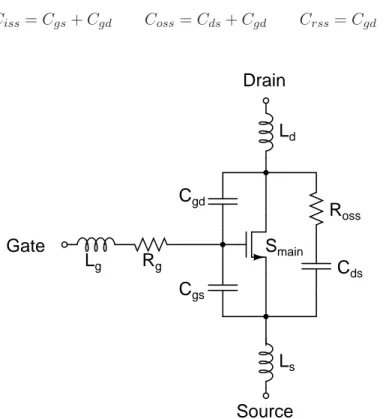
Whereas this is an acceptable trade-off at lower frequencies, large parasitic capacitances become the limiting factor of performance when the operating frequency approaches the VHF range. Figure 4.1 shows a schematic drawing of a MOSFET with the most important parasitic elements shown as discrete components. The inductors Ld, Ls, and Lg represent
the inductance of the bond-wires, packaging, and on-chip metallization. Rg represents the
parasitic gate resistance, which can be several Ohms in some cases. Ross is the equivalent
series resistance of the parasitic capacitance between the drain and source terminals. The model of Figure 4.1 does not include the parasitic output resistance of the gate-to-drain capacitance. For the transistors covered here, Cgd is substantially smaller than Cds, such
that the effect of this resistance can be ignored for simplicity. The parasitic capacitances Cgd, Cgs and Cds are often listed in device datasheets in terms of Ciss, Coss and Crss. The
relationships between the parameters are: Ciss= Cgs+ Cgd Coss= Cds+ Cgd Crss= Cgd (4.1)
C
dsR
ossC
gdC
gsL
dL
sL
gR
gSource
Gate
Drain
S
mainFigure 4.1: Schematic drawing of power MOSFET with key parasitic element shown as discrete components.
4.1.1 Vertical Power MOSFETs
Most traditional power converters employ vertical power MOSFETs, which can provide ex-ceptionally low on-state resistance. To investigate the feasibility of using a vertical power MOSFET in a VHF converter, an extensive search for suitable devices was performed. Al-though eventually the decision was made to employ a lateral device (covered in Section 4.1.2) for the converter of this thesis, the device comparison and evaluation of vertical devices are presented here for completeness. Additionally, it is the hope of the author that the data presented in this section may be of use for future converters where different design specifi-cations can tip the scale in favor of vertical MOSFETs. In particular, the measured device parameters that are not listed on datasheets represent a considerable amount of work. It is anticipated that their listing here will reduce the design time of future converters utilizing
similar devices.
As is shown in Chapter 5, a resonant gate drive circuit is beneficial for VHF operation. It can be shown [16, 41] that the loss associated with a sinusoidal resonant gate drive is given by:
Pgate= 2Rgπ2f2Ciss2 Vg,ac2 (4.2)
Here Vg,ac is the amplitude of the sinusoidal ac voltage, Rg is gate resistance, Ciss is device
input capacitance, and f is switching frequency. Rg, the gate resistance, constitutes the
equivalent series resistance (ESR) of the input capacitance together with any additional series resistance of the drive circuit. This is a parasitic that does not affect gating loss in hard gating, but it is an important parameter when selecting transistors used for resonant gating. Unfortunately, Rg is rarely listed on device datasheets, so this value has to be
measured for each of the device candidates.
One other major device-loss of soft-switching converters is conduction loss. This is the ohmic loss due to the non-zero resistance of the transistor during its on-state, and is given by:
Pconduction= IRM S2 Rds,on (4.3)
As Equations 4.2 and 4.3 show, three important device parameters that govern power loss of VHF resonant converters using vertical MOSFETs are Rg, Ciss, and Rds,on. A useful
metric for evaluating vertical devices is therefore to minimize RgCiss2 and Rds,on.
Table 4.1 provides measured data for a number of 60 V vertical power MOSFETs from various manufacturers. The measurements were done in the following manner: the input capacitance Ciss was measured using an Agilent 16092A spring clip fixture attached to an
Agilent 43961A RF impedance adapter on an Agilent 4395A impedance analyzer. For this measurement, the drain and source of the device were shorted together, and the gate and source terminals were connected to the spring clip fixture. By measuring the magnitude and phase of the DUT’s response to an applied test signal, the impedance analyzer calculates the capacitance and resistance of the connection (Ciss and Rg for this measurement setup).
This is done over a sweep of frequencies. Table 4.1 lists the values of Ciss and Rg measured
for a frequency of 30 MHz. The on-state resistance, Rds,on is the temperature-adjusted
temperature (25◦
C) value of resistance has been adjusted for an operating temperature of 135◦
C according to the temperature dependence from each device’s datasheet (typically an increase in Rds,on of 60-100%).
Device: Ciss [pF] Rg[Ω] Rds,ona [Ω] Rg∗ Ciss[Ω nF2]
FDZ209 850 1.5 0.136 1.08 FDD5612 830 1.57 0.128 1.08 SUD23N06-31L 950 1.47 0.081 1.32 Si7850DP 1265 1.32 0.056 2.23 HUFA764 1000 2.3 0.101 2.30 FDS5690 1645 1.18 0.059 3.20 IRCZ34 2340 1.1 0.09 6.02 FDS5680 2311 1.19 0.038 6.36 FDS5672 2511 1.43 0.023 8.99 IRF7478 2635 1.51 0.053 10.5 FDS5170N7 3432 1.1 0.027 13.0 FDS5670 3572 1.26 0.031 16.1 IRF1010ES 5160 0.7 0.02 18.6 a
Rds,onobtained from device datasheets for Vgs= 6 V, temperature adjusted for a
temperature of 135◦C
Table 4.1: Measured device parameters for 60 V vertical MOSFETs
Figure 4.2, a visual representation of the data of Table 4.1, shows a scatter plot of all the devices in terms of the parameters Rg ∗ Ciss2 and Rds,on. The scatter plot provides a
visual means of estimating the relative “goodness” of devices. Using above loss metric, one would not, for instance, choose a device whose values of Rg and RgCiss2 are both larger
than those of another device. This can be easily seen by the distance from the origin in the x and y direction. One cannot, however, simply use the distance from the origin as a parameter to find the best device without knowing the relative contributions of gating loss and conduction loss to converter efficiency.
In order to identify the transistor most suitable for use in the converter presented in Chapter 3, an analytic expression for converter losses is useful1. Unfortunately, at this
1
It is possible to measure and completely characterize the parameters of each of the potential devices of Table 4.1. Subsequent converter design (according to the methodology outlined in Chapter 3) and computer simulation for each device would shed some light on the relative merits of the different transistors. However, this brute force approach, in addition to being hohorrendouslyime consuming, provides no design insights into the relative importance of the device parameters.
0 0.02 0.04 0.06 0.08 0.1 0.12 0.14 0 2 4 6 8 10 12 14 16 18 20 R DS,on [Ω] R g *C iss 2 [ Ω *nF 2 ]
60V scatter plot of loss parameters
FDD5612 FDZ209 SUD23N06 Si7850DP HUFA764 FDS5690 IRCZ34 FDS5680 FDS5672 IRF7478 FDS5170N7 FDS5670 IRF1010ES
Figure 4.2: Scatter plot of potential 60 V vertical MOSFETs.
time no such expression exists for the topology presented in Chapter 3. Therefore the exact relative contribution of the parasitic parameters Rg, Ciss, and Rds,onto converter loss
cannot be found. However, the inverter of Chapter 3 shares many characteristics with the well-studied Class E inverter [20]. Therefore, the analytic expressions [20, 38, 43, 44] for the Class E inverter can be used to evaluate the relative merits of the devices listed in Table 4.1 when used in a VHF resonant inverter topology similar to the Class E inverter. It has been found [38, 41] that the normalized conduction loss for the Class E converter is given by:
2.363Rds,on
V2 cc
P (4.4)
where Vcc represents the dc input voltage.
Normalizing Equation 4.2 for output power, and adding it to Equation 4.4, results in the the following expression for normalized power loss : [41]
Pnorm= 2.363Rds,on V2 cc P + 2Rgπ 2f2C2 issVg,ac2 P (4.5)
Taking the derivative with respect to P of above function, one finds that the minimum normalized power loss occurs when the gating loss and conduction loss are equal.
The analysis above identifies the optimum operating power level to maximize efficiency of a Class E based converter with a certain device at a given frequency. Since it is desirable to operate at the highest achievable frequency, a metric to compare device performance for different frequencies is needed. A useful comparison is to operate each device at the optimal power level as given by Equation 4.5, and calculate normalized power loss for varying frequencies. It is expected that devices with lower Rg and Ciss will perform better
at higher frequencies, since the frequency-dependent gating loss should increase less rapidly. Figure 4.3 shows a normalized loss vs. frequency plot for selected 60V MOSFETs.
100 101 102 0 0.02 0.04 0.06 0.08 0.1 0.12 0.14 0.16 0.18 0.2 Frequency [MHz] Normalized Loss Device Losses: V DSmax = 60 V, VGS,ac = 7 V IRF1010ES IRCZ34 FDS5680 2N7002 (ST) FDS5690 FDS5670 FDS5672 IRF7478 FDS5170N7 FDZ209 HUFA764 Si7850DP SUD23N06−31L FDD5612
Figure 4.3: Plot of normalized power loss vs. frequency for 60 V vertical MOSFETs.
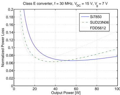
From Figure 4.3 it is evident that many devices are ill-suited for operation at VHF frequencies (30-300 MHz) due to the rapidly increasing gating loss. Considering a desired operating frequency of above 25 MHz (to achieve component miniaturization) and a desired device loss below 10% (to achieve high efficiency) it can be observed that there are a handful