Quantitative Nano-Analysis of Superconducting Materials via SEM-FIB 3D-EDS
Tomography.
Giuseppe Pavia1, Martin Kienle1, Ingo Schulmeyer1, Frank Bauer2, Marco Cantoni3, and Ken Lagarec4
1.
Carl Zeiss Microscopy GmbH, Product Management Materials, Oberkochen, Germany. 2.
Oxford Instruments GmbH, Wiesbaden, Germany. 3.
EPFL, CIME, Lausanne, Switzerland. 4.
FIBICS Incorporated, Ottawa, Canada.
The final goal of any investigation about the world surrounding us, animated or unanimated, is to have a better understanding of it, about its structure, composition, and behavior. The present investigation target is pushed down to nanoscale features, where the assumption of homogeneity fails dramatically, both for living and inanimate structures. 3-dimensional (3D) investigation is henceforth more and more necessary and required. The advent of FIB-SEM microscopes has been crucial for providing large scale availability of 3D tomography at the nanoscale level. Energy Dispersive X-ray microanalysis (EDX) has been since long time a principal investigation method due to the ability to determine composition with a good accuracy. Latest large area Silicon Drift Detectors (SDD) has drastically increased the acquisition speed and with that the ability to analyze bigger portions of a sample. The excellent resolution of modern FIB-SEM instruments also at high currents contribute also to faster 3D EDX analysis
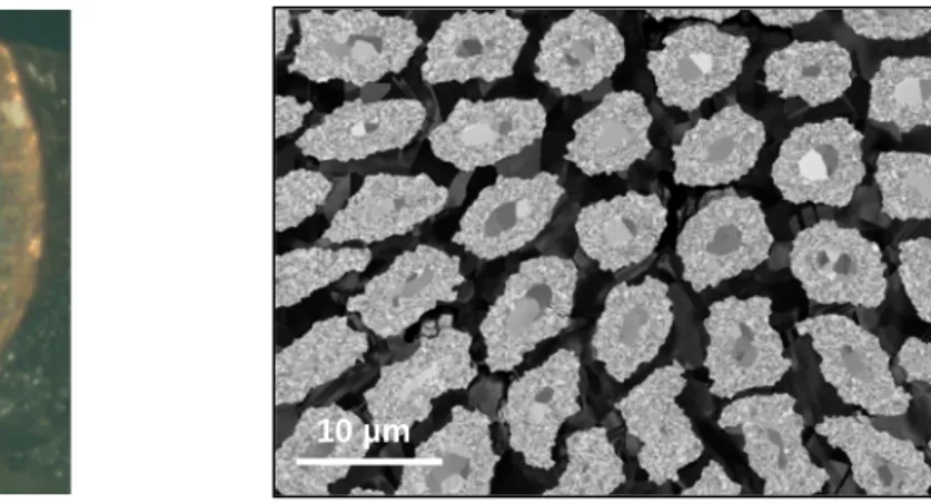
We present here our studies about the structure of a superconductor cable. It has a multifilament structure with about fourteen thousands of Nb3Sn filaments, with an average diameter of about five micrometers each, embedded in a bronze matrix. The sample was first investigated at the macro scale, with optical instrumentation, from macro photography to optical microscopy. The sample surface and cross section show features helping to identify suitable regions of interests, that are selected for being observed in more detail and with different contrast mechanisms with SEM imaging. During this process of progressive targeted reduction of the investigated area size, it is possible and useful to spatially correlate large area scale images with images taken at larger magnification and resolution, and even with the results of microanalysis investigation.
For the acquisition of the 3D EDX dataset we use a Zeiss Crossbeam 540, equipped with an Oxford Instruments X-Max 100 EDS SDD. Goal of this study is to get a better understanding of the sample by correlating optical images with electron microscopy images and the information provided by the chemical EDX analysis. The 3D dataset is acquired by serial sectioning using the ion beam and secondary electron and backscattered imaging combined with EDX analysis of the cross-sections. The setup allows to individually set up the parameters for all relevant milling, imaging and EDX parameters.
Paper No. 0670 1341
doi:10.1017/S1431927615007497 © Microscopy Society of America 2015 Microsc. Microanal. 21 (Suppl 3), 2015
https://doi.org/10.1017/S1431927615007497
Figure 1. Left to right: optical image and SEM image of the sample.
Figure 2. Acquisition Geometry
Figure 3. Left to right: 3D maps of copper, niobium, and tin; composite map superposed to SEM
image. I-beam e-beam EDX Cu Nb Sn 10 µm 1342 Microsc. Microanal. 21 (Suppl 3), 2015
https://doi.org/10.1017/S1431927615007497