Analysis of Terabit/Second-Class Inter-Chip Parallel
Optoelectronic Transceiver
by
Nguyen Hoang Nguyen
MASSACHUSETTS INSTITUTE
OF TECH4OLOGY
NOV 19 2010
LIBRARIES
ARCHIVES
B.Eng. (Hons), Electrical Engineering, National University of Singapore, 2009SUBMITTED TO THE DEPARTMENT OF MATERIALS SCIENCE AND ENGINEERING IN PARTIAL FULFILLMENT OF THE REQUIREMENTS FOR THE
DEGREE OF
MASTER OF ENGINEERING IN MATERIALS SCIENCE AND ENGINEERING
AT THE
MASSACHUSETTS INSTITUTE OF TECHNOLOGY
SEPTEMBER 2010
© 2010 Massachusetts Institute of Technology
All rights reserved.
Signature of Author...
44 nt of Material' ScIence and Engineeriiig August 12, 2010 Certified by...
Lionel C. Kimerling Thomas Lord Professor of Materials Science and Engineering A Thesi5S&uppisor A ccepted by... -. ...
Christopher Schuh Chair, Departmental Committee on Graduate Students
Analysis of Terabit/Second-Class Inter-Chip Parallel
Optoelectronic Transceiver
by
Nguyen Hoang Nguyen
Submitted to the Department of Materials Science and Engineering on August 12, 2010 in Partial Fulfillment of the
Requirements for the Degree of Master of Engineering in Materials Science and Engineering
ABSTRACT
Electrical copper-based interconnect has been suffering from fundamental physical loss mechanism and its current infrastructure will not be able to meet the increasing demand for data rates due to reaching the limit of the transmission bandwidth-distance product. Optical interconnect has been known as the candidate for taking over the obsolete electrical counterpart owing to the capability of transmitting data at high rates with low loss and the feasibility for parallel integration. Optoelectronic transceiver is one of the essential elements in optical interconnect system. This thesis scrutinizes a complete set of constituent technologies developed for a novel inter-chip parallel optoelectronic (OE) transceiver (known as Terabus transceiver) which is able to communicate data at the speed in the range of Terabit/second.
A novel packaging hierarchy and a creative design for an optical coupling mechanism devised to
bring high-level integration and high-speed performance to a final package have been analyzed: Two 4x12 arrays (each < 9 mm2) of CMOS transmitter and receiver ICs have been flip-chip
bonded to a silicon carrier interposer of 1.2-cm2 size. Other two 4x12 arrays of OE devices (VCSELs and photodiodes) with comparable size are then flip-chip bonded to the corresponding
CMOS arrays attached to the silicon carrier, forming the Optochip assembly. The Optochip is in
interface with an Optocard by the flip-chip bonding process between the silicon carrier and an organic card patterned with 48 integrated waveguides at density of 16-channel/mm and total length of 30 cm. The 985-nm operating wavelength of the lasers allows a simple optical design with emission and illumination through arrays of relay lenses directly etched into the backside of the OE Ill-V substrate. A novel design of 45*-tilted and Au-coated mirrors fabricated in 125-ptm-pitch acrylate waveguides is to perpendicularly couple the light in and out of the core of these Optocard waveguides. Per-channel performance of up to 20 Gb/s for transmitter and of up to 14 Gb/s for receiver have been realized.
Lastly, the thesis has analyzed the market opportunity of the transceiver by reviewing the market situation, identifying contemporary competing technologies, assessing the market prospect and predicting the cost.
Thesis Supervisor: Lionel C. Kimerling
Acknowledgements
I would like to take this opportunity to express my heartfelt gratefulness to whom by one way or
another have provided me with support in the process to complete this thesis. Without the support, definitely, it would be pretty much impossible for me to complete this thesis with success.
First of all, I would like to thank Professor Lionel Kimerling for offering me a project to fulfill my M.Eng degree at MIT. I wanted a project which has both materials science and electrical/optical engineering in nature then I got. In both of the two meetings we went through at MIT, I was always given with patient guidance as well as valuable suggestions and recommendation for research from Prof Kimerling. I would like to thank MIT Materials Processing Center for offering me access to the CTR and Industry Consortium website from which I can approach the most up-to-date technology information in the field which is undeniably integral to the thesis.
I would like to thank Professor Chua Soo Jin from the National University of Singapore (NUS)
for a timely discussion we had near the start of my final MIT M.Eng semester in Singapore, which helped me narrowing down the thesis topic and also for his enthusiastic guidance during the course of my thesis.
I would like to appreciate Mr Nguyen Xuan Sang, SMA direct PhD 2008, for his support in
selecting and introducing references and for the discussions through which I have gained understanding and knowledge in nanomaterial processing.
I would like to thank Ms Lisa, Prof Kimerling's assistant for helping out dealing with logistic
issues and delivering the thesis hardcopies to the Academic Office.
I would like to appreciate the support and understanding from the HR personnel manager at
Schlumberger Singapore where I have been doing the internship since the last 2 month of thesis completion.
I would like to thank my Singapore-MIT Alliance classmates, AMM&NS 2009 intake, for the
time we have experienced throughout the SMA 09-10 journey. Without the classmates, my SMA Dual Masters "challenge" would not be as memorable as it is.
I would like to appreciate the encouragement and understanding from my girlfriend, Le Khanh.
She has encouraged me to get through hard and depressing moments of the thesis. For me, this thesis is indeed unforgettable.
Last but not least, I would like to thank my family for the enduring encouragement and indispensable support without which I would not be able to achieve what I have accomplished by now.
Table of Contents
PART I
Background of Silicon Microphotonics and Optoelectronic Transceiver Fundamentals.... 12
CHAPTER 1: The coming Regime of Silicon microphotonics...13
1. Why Silicon Microphotonics? ... . . . .. . . .. . . . 13
2. Roadmap for Silicon Microphotonics...15
CHAPTER 2: Optoelectronic Transceiver Fundamenta ... 17
1. Overview... - - ... 17
2. Parts of Optoelectronic Transceiver... 18
a. Optical Laser Source Technology...18
Light Emitting Diode (LED)...18
Edge-Emitting Laser (EEL)... 19
Vertical Cavity Surface Emitting Laser (VCSEL)...19
Key Competitive Laser Source Technology...20
Key Power Module Technology for Laser Source...21
Recent Research Breakthrough in Ge Laser Source...22
b. Optical Detector Technology...22
Key Technology to Improve Responsiveness...23
c. Modulator Technology...24
d. Packaging Technology... 25
e. Monolithic Integration Consideration...25
PART II Terabit/Second-Class Inter-chip Parallel Optoelectronic Transceiver...27
CHAPTER 1: Overview of the Terabus Transceiver...28
1. Background... - ... 28
CHAPTER 2: 2-D Arrays of VCSELs and Photodiodes
CMOS Transmitter Driver Circuits and Receiver Circuits... 32
1. Vertical Cavity Surface Emitting Lasers... 32
2. Photodiodes...33
3. CMOS IC Arrays of VCSEL Driver Circuits and Receiver Circuit...34
a. CMOS VCSEL Driver Circuits...34
b. CMOS Receiver Circuits...35
CHAPTER 3: Silicon Carrier Optochip Assembly, Optocard Optical Coupling and Alignment, Packaging...37
1. Silicon C arrier...38
a. Structure and Function...38
b. Fabrication and Processing...39
2. Optochip Assembly, Optocard...42
a. Optochip Assembly...42
b. O ptocard...44
3. Optical Coupling and Alignment, Packag g...45
a. Optical Couple and Alignment... 45
i. Optical Coupling Mechanism... 45
ii. Study for Tolerance of Optical Alignment...47
b. Packaging... 48
i. Optochip-to-Optocard Packaging...48
ii. Thermal-Control Consideration for the Package...49
CHAPTER 4: Results and Evaluation...51
1. Measurement of Silicon Carrier Electrical Signal Path...51
a. Measurement of Differential Microstrip Lines on Silicon Carrier...52
2. Measurement of Optocard Waveguide for Loss and Dispersion...55
a. Optocard Waveguide Loss Measurements...55
b. Optocard Wveguide Dispersion Measurement ... 55
3. Optochip Characterization...57
Crosstalk Consideration... ...58
Power Consumption budgeting consideration...43
PART I Market Opportunity... ... 61
CHAPTER 1: Market Analysis... ... 62
1. The Supercomputing Market... ..62
2. The need for standardization of inter-chip transceiver market...65
3. Competing Technologies... 66
a. Electrical Copper-based Interconnect Technologies...66
b. Optical Interconnect Technologies...68
The Intel Light Peak...68
The Japan Project...69
4. Thoughts on the market prospect of optical interconnect/transceiver...71
CHAPTER 2: Production Cost Model...73
1. The Process-Based Cost Model...73
2. Case Study: The Cost Model of the Optoelectronic Transceiver...76
a. Attributes and Parameters...76
b. Process Flow for the Terabus Transceiver...78
c. The Economies of Scale...81
PART IV Conclusion and Recommendation for Future Work...86
References... ... 89
List of Figures
Figure 1: Electronics-photonics domain transition border [1]... 13
Figure 2: Elements of an optical link [courtesy Intel]...15
Figure 3: Roadmap for Silicon microphotonics [Courtesy MIT CRT] [1]...16
Figure 4: Functional Block Diagram of a typical optoelectronic transceiver...17
Figure 5: Structure of an edge-emitting laser [2]...19
Figure 6: Structure of a vertical cavity surface emitting laser [3]...20
Figure 7: Laser built from germanium for optical communication, courtesy: MIT EMAT group [4]...22
Figure 8: P-I-N photo detector...22
Figure 9: Structure for laterally-coupled germanium diodes [1]...23
Figure 10: Optoelectronic modulator [courtesy MIT]...24
Figure 11: Packaging for optoelectronic transceiver...25
Figure 12: Monolithic LED on Si substrate with CMOS technology [6]...26
Figure 13: Schematic of Terabit/s package composed of Optocard with waveguides and transceiver Optochips [10]...29
Figure 14: Structure of Terabus/second transceiver [14]...31
Figure 15: Schematic (left) and photograph (right) of bottom-emitting VCSEL [15]...32
Figure 16: Enlarged eye diagrams of 6-pim VCSELs at 10 and 20 Gb/s (70"C) [15]...33
Figure 17: Frequency response of photodiodes with different diameters at 1.5-V reverse bias [10]... . . 33
Figure 18: Functional block diagram of a single-channel VCSEL driver IC [16]...35
Figure 19: Functional block diagram of a single-channel receiver IC [18]...36
Figure 20: Top view of silicon carrier layout (left); structure of the transceiver (right)... 37
Figure 21: Silicon carrier process flow [14]...- ... 39
Figure 23: Top view of 3 wiring levels on top of silicon through vias: signal, power and ground
[14]... 41
Figure 24: Solder micro bumps and array [20]...43 Figure 25: Flip-chip assembly procedure (left). Bottom view of Optochip: OE in cavity and
UBM pads (right)...-.- 44
Figure 26: Layout of the Optocard (left) and cross-section with 62.5-ptm-pitch integrated waveguides (right)
(IBM)... 44
Figure 27: Optical coupling mechanism between OEs and the Optocard waveguides...45 Figure 28: Schematic diagram of mirror fabrication at the end of 48 Optocard waveguides (left). Photograph of fabricated sample illuminated by a white light (right)...46 Figure 29: Coupling efficiency of VCSEL (up) and Photodiode (down) to waveguide vs.
horizontal offset (x-y) [14]. ... 47
Figure 30: Entire Optochip-on-Optocard assembly (left) and bottom view of silicon carrier
(right)... ...--... 49
Figure 31: 3mm heat pipe in contact with test chip [23]...49 Figure 32 a : Temperature distribution in test chip with no cooling (left) and result for
temperature distribution in the entire package (right) [23]...50 Figure 32 b: Local temperature distribution in the VCSEL chip with no cooling (left) and with heat pipe cooling (right) [23]... 50
Figure 33: Electrical path (in red) on silicon carrier: strip line on the Optocard and silicon carrier through via, m icrostrip line [14]...51 Figure 34: Layer dimensions of differential microstrip transmission lines on the silicon carrier (left) and its eye diagram (right) for 7-mm length at 20 GHz, PRBS 7-1 data pattern [14]...52 Figure 35: S-Parameters (SnI and S12) of the 7-mm silicon carrier microstrip line...53 Figure 36: Measurement setup for silicon carrier through via transmission [14]...53 Figure 37: Transmissions of the through via + the 7-mm Optocard line (red) and of the reference Optocard line only (blue)... ....54 Figure 38: Impulse response measurement of a 1-m multi-mode polymer optical waveguide at input and output (left). Evolution of Images of the single-mode fiber launch into the waveguide due to dispersion (left) [26]... . ... 55 Figure 39: Summary of pulse broadening results for 8, 17, 100 and 255-cm waveguides for both
Figure 40: Eye diagram at 20 Gb/s from a Terabus transmitter. The drive circuit included a
circuit to compensate for the fall time of the VCSEL emission [26]...57
Figure 41: Received eye diagram of a transmitter Optochip to receiver link at 14 Gb/s (left). 10 Gb/s received eye diagram using low power variant circuits and reduced supply voltages [26]..58
Figure 42: Power consumption per bit rate for a single-channel 10-Gb/s error-free multi-mode fiber link. Inset: received eye of the 48 mW (22 mW for transmitter and 26 mW for receiver) link. [10]... . . .. 59
Figure 43: Performance of the fastes computer systems for the last six decades compared to M oore's law [28]...62
Figure 44: Main active players in high performance computing market throughout time [28] ... 63
Figure 45: Top 500 supercomputers by nations...64
Figure 46: PCI Express slots (from top to bottom: x4 , x16, x1 and x16)...67
Figure 47: Light Peak technology (Intel)...68
Figure 48: Configuration of CPU-memory optical interconnection [35]...70
Figure 49: Transceiver fabrication process flow...80
Figure 50: Unit cost vs. annual production volume for the 3 scenarios given in the report [37]..81
Figure 51: The transceiver cost sensitivity to annual Production Volume...83
Figure 52: Top 10 process driving cost for the Terabus transceiver at 30,000 units annually...84
Figure 53: Terabit/s Transceiver Integration hierarchy [26]...86
Figure 53: Terabit/s Transceiver Integration hierarchy [26]...93
List of Tables
Table 1: Comparison between two common EEL and VCSEL optical laser sources...18
Table 2: Standardization state for LAN optical connection (2008)...65
Table 3: Front-end process modules in a transmitter PBCM...74
Table 4: Cleaving and back-end process modules in a transmitter PBCM...75
Table 5: Process sub-model inputs (required for each process step, e.g., MOCVD)...75
Table 6: Financial Parameters Used for the Cost Model...77
Table 7: Operational Parameters Used for the Cost Model...77
PART I
BACKGROUND OF SILICON MICROPHOTONICS
And
CHAPTER 1: The coming regime of Silicon microphotonics
1. Why silicon microphotonics?
Electronic communication links are degraded by fundamental physical loss mechanisms including dielectric losses and skin effect losses which are all functions of distance and bandwidth. In addition, near/far end crosstalk and noise aggravate these loss mechanisms. There is the maximum communication rate subjected to losses and noise levels for a given signal strength as stated by Shannon's law. As the demand for ever increasing bandwidth communication proceeds, the communication capability of electronic-based link gets asymptotic to this fundamental limit. Switching to alternative communicating platform is the essential trend. For many industries, photonics platform is the choice to replace electronics platform when the limitation is reached. Figure 1 shows the transition border (the red zone) between these two platforms based up on bandwidth-distance product criteria.
Distance * Bandwidth Market Map
1 Thz
Photonics
100Ghz
Haul
Metro Net
1ea Free Area
I kz P - ac-DVI ae Net plane 100 Mhz 10 Mhz Electronic Domain 0.IM iM 10M 100M 1KM 10KM 100KM
Figure 13: Electronics-photonics domain transition border [1].
13
---As shown clearly, the Long Haul Net has been already in the photonics domain because of the high requirement for transmitting high bandwidth over long distance while conventional Cable is still in the electronics domain due to low requirement for high bandwidth transmission. Each of the above industries is increasing demand for bandwidth throughout the time, ultimately exhausting the practical capabilities of electronic-based solutions.
Challenge for the transition to take place is that: the advent of an optical replacement of suitable cost during this transition zone will enable earlier conversion, that's why the cost of photonic links will likely need to be competitive with the cost of copper-based counterparts. To make use of the economic advantage of silicon, the key to reduce cost will be monolithic integration, just as VLSI electronics. Integrated silicon microphotonics which is fabricated monolithically by CMOS process will achieve a complete set of microphotonics devices using available process in existing CMOS fabs.
The key drivers for silicon microphotonics which are bandwidth cost and bandwidth volume will increase pressure for monolithic photonics integration as well as for low cost and small form factor optical packaging and high-speed interconnect. Key discussed silicon microphotonics technologies which implement optical communication links would be receivers, transmitters, filters, packaging, source and integration strategies. The goal is that sources, detectors, and modulators, as well as passive components such as waveguides and filters are made from silicon or new photonics compatible materials, e.g. Ge, BaTiO3 etc, and acceptable dielectrics and metals.
Figure 2 schematically describes very well elements of silicon microphotonics technology required for a typical optical link.
Transmitter
Receiver
DATA 0Fiber"
Laser Fiter Modulator Photo
(adds tunability) (improved encoding) * Receiver ... *...
+ Drive + Transimpedance
Electronics Amplifier (TIA)
Figure 14: Elements of an optical link [courtesy Intel].
These element technologies are comprised of the followings:
e Integrated Receiver Technology e Modulator Technology
" Photonic Source Strategy " Filter Technology
e Packaging and Interconnect Technology
2. Roadmap for Silicon Microphotonics
According to Communications Technology Roadmap (CRT) and MIT Industry Consortium [1], the roadmap for silicon microphotonics is suggested as in Figure 3. There are several prominent characteristics of the roadmap listed as follow, noting that inter-step iterations are expected and essential for technology development:
" Steps in the roadmap illustrate a nature but not necessary linear
e Each block sets the foundation and justification for the subsequent block
" Subsequently blocks may uncover technology that impacts previous blocks 15
Silicon Microphotonics Roadmap
Figure 15: Roadmap for Silicon microphotonics [Courtesy MIT CRT] [1].
The strategy is that different companies will focus on different steps (blocks) in the roadmap, but work together to benefit from the infrastructure of other steps, forming the Microphotonics Industry Consortium.
CHAPTER 2:
Optoelectronic Transceiver Fundamentals
1. Overview
The basic function of an optoelectronic transceiver is to receive optical signal which is laser light, convert it into electronic digital signal in terms of binary sequences of Is & Os; and in the reverse order, convert binary sequences of Is & Os into corresponding optical pulses and transmit them. That's where the name transceiver comes from, reflecting the two-way function of the device which can be described as transmitter and receiver altogether.
DA OUT..
Optical Source
Power Control
Photo Detector
Figure 16: Functional Block Diagram of a typical optoelectronic transceiver.
A typical optoelectronic transceiver consists of 4 major parts: optical laser source, photo
detector, electronic modulator and power control unit. Photo detector receives optical variations and converts into voltage and/or current variations whereas, when control signal which is a sequence of binary numbers of 1 & 0 comes in, the modulator dictates the optical laser source to
send out corresponding optical signals. Short-range optoelectronic transceiver functions to receive and transmit optical signal in the range shorter than 1 meter.
2. Parts of Optoelectronic Transceiver a. Optical Laser Source Technology:
The key function of an optical laser source is to convert electronic signal into optical light. There the following 3 alternatives:
" Light Emitting Diode (LED)
e Edge-Emitting Laser (EEL)
e Vertical Cavity Surface Emitting Laser (VCSEL)
Table 1: Comparison between two common EEL and VCSEL optical laser sources.
Specification EEL VCSEL
Application Telecom Datacom
Active Region Confinement 300*400*0.07 3*3*0.07
Modulation Frequency 20GHz 120GHz
Threshold Current 20mA 0.5mA
Output Power 45mW 0.17mW
Power Efficiency 0.89A/W 11.76A/W
Key consideration for optical source in short range transmission would be modulation frequency and transmission power which are both determined by the size of the active region. With small active layer, the loss should be small, threshold current is reduced and modulation frequency would be larger.
Light Emitting Diode (LED):
LED has a simple structure which contains no confinement layer. Light can come out at
any position with a wide range of energy spectrum. As the result, power output for LED is high
and LED is suitable for display and lighting applications. Since the modulation frequency of
LED is relatively low, LED is simply not a good candidate for optical source in high-speed
transceivers.
Edge-Emitting Laser (EEL):
Top Metallic Proton Bombarded
Contact Semi-Insulating Bamer p+GaAs p AlGaAs Active Region n AIGaAs n GaAs Substrate Bottom Contact
Emitting Region
Edge Emitting Laser Diode
Figure 17: Structure of an edge-emitting laser [2].
In EEL, laser light is emitted laterally from the edge of the structure as shown as the emitting region in Figure 5. The active region is large enough to emit not too weak transmission power (-45mW, as can be seen in Table 1, but still much less than the transmission power of
LED, which is - 0.1W) while can still achieve relatively high modulation frequency (-20 GHz, as can be seen in Table 1, but still smaller than the modulation frequency observed in VCSEL. With that balancing between emission power and modulation frequency, EEL is now the current technology for telecommunication.
Vertical Cavity Surface Emitting Laser (VCSEL):
In this type of laser, the active layer is confined between two distributed Bragg reflectors (DBRs) which function as laser mirrors. Active area is further reduced by lateral oxidation
19
.. .... ...:: - " - -... ... ... .... . ... ..... . .. .... ... . ...
confinement, which significantly boosts up the modulation frequency capability (>100GHz) and reduces threshold current of the device down to several pA.
Light Output Electrode
Transverse Mode field
DBR Current* Confinement eW ddinal DBR e ve Layer otical cnfinement ... ... .. Substra
Figure 18: Structure of a vertical cavity surface emitting laser [3].
Having very high modulation frequency, VCSEL has been becoming the right choice for optoelectronic transceiver technology now and in future.
Key Competitive Laser Source Technology:
Two classes of technologies for active optoelectronics (laser sources) are emerging in research labs. Each involves semiconductor particles controllably made on the nanometer length scale: (1) Solution-processed devices using materials such as InAs, PbS, PbSe produce infrared lights and (2) Si-nanocrystal active devices which can be processed by existing CMOS-compatible technologies such as plasma-enhanced chemical vapor deposition (PECVD) to produce photoluminescence and electroluminescence [1].
Key Power Module Technology for Laser Source:
High-speed coherent sources have only been demonstrated through hybridization. In such cases, vertical-cavity surface-emitting laser or edge emitting laser are mounted on Si platform and coupled into appropriate waveguide [1]. Central photonic power source analogous to an electronic power supply may be cost effective, which could feed many ICs without a need for each chip to have its own laser. This benefit should be substantial in multi-link applications but may not be in single optical link. Direct modulation diode lasers (near source) will run at higher energy densities, and likely have lower reliability. Continuous wave lasers (far source) will need to be compatible with on-chip modulation, implying polarization, mode, loss and wavelength control.
Recent Research Breakthrough in Germanium Laser Source:
MIT researchers from the Electronic Materials Research Group (EMAT) led by Professor Lionel C. Kimerling have demonstrated the first laser built from germanium that can produce wavelengths of light for optical communication [4]. It is the first germanium laser to operate at room temperature. Different from other typical materials for lasers, germanium is easy to be integrated into existing processes of silicon chip manufacturing. Since the addition of germanium increase the speed of silicon chips (germanium has carrier mobilities larger than those of silicon), incorporating germanium into the manufacturing process is what almost all chip manufacturers have already done or started to do. This germanium-laser project which is carried out by the group has opened up the new level of monolithic integration for silicon microphotonics.
Figure 19: Laser built from germanium for optical communication, courtesy: MIT EMAT group [4].
b. Optical Detector Technology
The key function of photo-detector for optical communication is to convert received optical signals into electrical forms, i.e. either voltage or current variations, for subsequent amplification and signal processing. The P-i-N photo detector consists of 3 layers: intrinsic layer 'i' sandwiched in between the 2 layer semiconductor n-type and p-type to enhance carrier generation by photon stimulation. Incident photons absorbed across the 'i' region would generate electron hole pairs (Figure 8). With voltage bias, these carriers are swept to the p and n regions and get recombined. As the result, the net current exists in the closed circuit. That's fundamentally how optical signal is converted into electrical current by a photo-detector.
Camenr are colle ced iro tht deplIon reg on
Figure 20: P-I-N photo detector. 22
Key Technology to Improve Responsiveness of Short-Range Detector by increasing Carrier Mobility:
With Ge on strained Si technique, modulation frequency up to 10GHz has been realized and especially the fabrication is compatible with existing CMOS infrastructure and supply chain. Research is uncovering a variety of way to utilize silicon platforms in receiver (detector) technology while hybridized mounted detectors have already been commercialized. Si itself is a rather poor absorber, i.e. its absorption depth is large, at most popular communication frequencies (>1Im). Short germanium absorption depths open the possibility of normal incidence coupled detector diodes, and the responsiveness of Ge extends into longer communication wavelengths especially under strain condition. Higher mobility of Ge allows even faster response.
Key question for silicon receivers is how to interface them to multi-mode fiber for normal incidence diode structures. Addition question for Ge is whether the intrinsic silicon lattice mismatch (4%) can be managed over noise [1].
Figure 21: Structure for laterally-coupled germanium diodes [1].
c. Modulator Technology
Sio2
Figure 22: Optoelectronic modulator [courtesy MIT].
In silicon plasma modulator approach [1], silicon waveguide channel is flooded with carriers which alter the channel's refractive index. This variation of refractive index can be utilized in Mach-Zender interferometer structures to create light amplitude modulation. In other approach using electro-optic material such as barium titanate (BaTiO3) for modulators, the materials deposited on a buffer layer of magnesium oxide have shown some compatibility with standard silicon processing techniques. In other modulator research regarding quantum well structures in materials, Si nanocrystals on SiO2, for example, have shown electroluminescence and electro-absorption. Although still early in research, this is a possible solution for modulators as well as Si laser source.
Key remaining challenge for the current optoelectronic modulator technology is that Si plasma modulation and Si receiver are not likely compatible with each other. Plasma modulator probably needs Ge diode. Electro-optic materials like BaTiO3 are still very much in question to be integrated with standard Si processing.
---d. Packaging Technology
It is essential that all components discussed above would be able to be assembled into one highly small compact package. Package for discrete optical source or detector could be either ROSA or TOSA as shown in Figure 11. All of the components are finally put on same substrate and form the product. One of promising alternative technologies is parallel assembly which is ideal for VCSEL since light is emitted vertically [5].
LED i PhMOd Reoptoc* (CAI
XTrapow
psafts
ROSA '-a
I-TF, Rx
Figure 23: Packaging for optoelectronic transceiver.
e. Monolithic Integration Consideration for Optoelectronic Transceiver
It is the key for silicon microphotonics that devices are built entirely on the Si substrate which can be fabricated using traditional CMOS processing techniques. Monolithic LED has been realized so far. Results of current research on edge-emitting laser (EEL) and vertical cavity surface emitting laser (VCSEL) show that monolithic integration for these optoelectronic devices are highly promising.
amn
Parallel assembly
CMOS LED
Transistor i
PART II
TERABIT/SECOND-CLASS INTER-CHIP PARALLEL
Overview of the Terabus Transceiver
1. Background
In the context of current technology, interconnect bandwidth requirements within high-performance computing systems keep increasing. This common trend is driven strongly by the ever-increasing processor speeds, number of processors per system and wide data bus capacity. Parallel optical interconnect between different blocks of the same circuit board or inter-board through back plane is very promising in terms of data throughput, integration density, power consumption and loss optimization as well as latency. With optical interconnect, the constraint on communication link length is undeniably much more liberated in contrary to electrical (copper) counterpart. Parallel optical interconnects based on multimode fibers with total data rates in the range of 100 Gb/s have been increasingly utilized over the next few years or more for links between racks of servers or between boards over lengths from one meter up to hundreds of meters. The debate now is on when optical interconnect will penetrate further within the board for chip-to-chip communication. The competition between optics and copper-based electrical backplanes for on-board interconnects is comprehensive in terms of speed, power efficiency, form factor and, last but not least, cost especially in the light of the advance in high speed electrical interconnects [7], [8]. It is obvious that there exists a critical bandwidth-length product above which optics is favorable because of power consumption [9] and signal integrity.
The key discussion topic for developers now is which interconnect architectures would significantly benefit from the high bandwidth and high level of density that optical technologies have to offer.
2. Introduction of the Transceiver
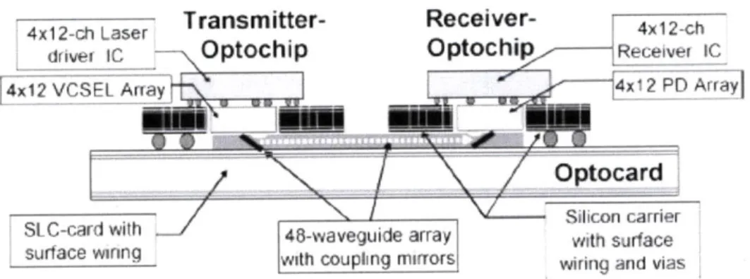
As one of excellent optical interconnect architectures, the Terabit/second-class inter-chip parallel optoelectronic transceiver has been developed under the IBM Terabus project. A complete set of technologies [10] has been proposed and developed to support terabit/second inter-chip data transfers over organic cards within high-performance servers, switch routers, and other intensive computing systems. The transceiver architecture (Figure 13) comprises of a chip-like optoelectronic packaging structure (Optochip), assembled directly onto an organic card (Optocard). In order to reduce the size and boost up the speed, integration parallelism is utilized such that the data rate per line is pushed up to 20 Gb/s and the total number of channels in the bus is designed to be 48 (4x12), achieving the overall data transfers in the range of 0.5-1 Th/s. The 4-by-12 arrays of 985-nm vertical-cavity surface emitting lasers (VCSELs) and photodiodes (PDs) are flip-chip bonded to the corresponding driver and receiver IC arrays which are implemented by 130-nm CMOS technology. These 2 IC arrays are in turn flip-chip assembled onto a 1.2-cm2 silicon carrier to complete the transceiver Optochip. One thing needs to be clear here is that the latter flip-chip process is carried out first and then followed by the former due to ease of fabrication which will be discussed subsequently in details.
Transmitter-
Receiver-4x12-ch Laser U4I12-ch
driver Ic Optochip Optochip Receiver IC
IWx2 VCSEL Array 4x 12 PD_ Array
Optocard
St CcardwithSilicon carrier
surface winh 48-waveguide array with surface with coupling mirrors wiring and vias
Figure 13: Schematic of Terabit/s package composed of Optocard with waveguides and transceiver Optochips
[10].
The silicon carrier has electrical through vias, high speed wiring and the 1.5 mm x 4.2 mm rectangular cavity to house the VCSEL and PD arrays. This 1.2-cm2-form-factor Optochip module aimed for low-power operation will transmit the data through a 62.5-pm-pitch array comprised of 48 parallel multimode optical waveguides patterned on the Optocard. A novel scheme for optical coupling between the Optochip and Optocard has been developed in which the optoelectronic (OE) arrays, which comprise of VCSELs and PDs, are backside emitting or illuminated through arrays of antireflection-coated micro-lenses etched onto the backside of the
OE substrates. Right under the OE devices and inside the waveguides on the Optocard, 450-tilted mirrors are subtly fabricated to creatively couple the light into and/or out of the array of waveguides (Figure 13).
Single channel has been demonstrated to operate up to 20 Gb/s for transmitter and 14 Gb/s for receiver. The per-channel power dissipation over multimode fiber is observed to be as low as 50 mW for 10-Gb/s single-channel links [10].
The Terabus project has been successful in designing the novel Terabit/s-class OE transceiver with prominent features: high bit rate, high level of channel density, which improved the device form factor, and low power consumption. Subsequently, to compete with purely electrical counterparts, highly reliable and cost-effective prototypes are essential. Therefore, the option criteria for electrical packaging, designs of IC and OE devices, waveguides and optical coupling are recommended as follow [10]:
" Utilization of flip-chip technology to reduce wire-bond parasitics.
e The choice of surface-laminar-circuitry (SLC) as an organic card for the Optocard to make use of high wiring density [11].
" Use of Si carrier interposer for Optochip packaging due to the through vias allow direct
solder attachment of the Optochip and the Optocard and dense wiring connected to the ICs on top of the interposer [12].
* Use of CMOS ICs to optimize IC power efficiency and cost.
* Option of operating wavelength of 985 nm to allow simple optical design based upon the Ill-V GaAs/InP substrate and to permit direct integration of lenses onto the backside of the substrate [13].
Figure 14: Structure of Terabus/second transceiver [14].
The subsequent sections will analyze the high-speed OE transceiver in details regarding: components and circuits; fabrication, alignment and packaging; as well as optical, electrical characterization, results and evaluation. The structure is as follow:
" 2-D arrays of VCSELs and PDs; CMOS transmitter driver circuits (TX) and receiver
circuits (RX).
* Silicon carrier; Optocard; optical coupling and alignment; packaging.
CHAPTER 2:
2-D Arrays of VCSELs and Photodiodes
CMOS Transmitter Driver Circuits and Receiver Circuits
1. Vertical Cavity Surface Emitting Lasers
polyimide
Sem-insiuatng Substrate AR coating
Figure 15: Schematic (left) and photograph (right) of bottom-emitting VCSEL [15].
The schematic of the bottom-emitting 985 nm VCSEL structure is shown in Figure 15. The structures were grown on semiconductor GaAs substrate with low-pressure metal-organic chemical vapor deposition (MOCVD) reactor. The epitaxial structure consists of 27.5 pairs of n-type GaAs/Alo.9Gao.1As bottom distributed Bragg reflector; 1- cavity with multiple quantum well active region and 40 pairs of p-type Alo.1Gao.9As/Aso.95Gao.05 top distributed Bragg reflector
[15]. The device have an oxide-confined structure which is optimized for low series resistance,
low parasitics and high-speed operation at low current density while minimizing the excess free carrier loss to the device. The multiple quantum well active region contains three strained InGaAs/AlGaAs quantum wells and two thick graded AlGaAs layers to add up to the cavity thickness [15].
The VCSELs with apertures of 4, 6 and 8 pm are fabricated and optimized for 700 - C
operation [10]. An array comprised of 4x12 VCSELs is fabricated. The VCSELs with diameter of 4 pm and 6 pm have bandwidths all above 15 GHz and biasing currents of 2mA and 3mA
respectively [15]. All 48 VCSELs are identically modulated and each channel has extinction ratio above 6 dB.
VCSEL
@
1OGb/s, 70
0C
VCSEL
@
20Gb/s, 70"C
20 ps/div 20 ps/div
Figure 16: Enlarged eye diagrams of 6-pm VCSELs at 10 and 20 Gb/s (700 C) [15].
Figure 16 illustrates 10 Gb/s and 20 Gb/s eye diagrams of a 6 im VCSELs operating at 70*C.
2. Photodiodes
Photodiodes with mesa structure are grown on Fe-doped InP substrate and are backside illuminated. The device responsivity is extremely sensitive to optical absorption in the p-InGaAs layer, requiring this layer to be as thin as possible. 4 sizes of 30, 40, 50 and 60 jim are fabricated for the 2-D 4x12-photodiode array. The frequency response is calculated from Fourier transform of impulse response measurements with 2-ps pulses at 985 nm.
-0- 30um diameter
A 50um diameter
* 60um diameter
1.0 10.0 100.0
Frequency [GHz]
Figure 17: Frequency response of photodiodes with different diameters at 1.5-V reverse bias [10].
33
Figure 17 shows the inverse relationship between the 3-dB cutoff bandwidth and the diameter of the photodiode, i.e. the smaller the size, the larger the bandwidth, thus the better. At
1.5-V reverse biasing, 60-pm photodiode has 3-dB cutoff bandwidth of 13 GHz while 30-gm
photodiode has the one of 30 GHz which is much larger. However, the smaller the size the better tolerance is required; therefore trade-off between bandwidth and tolerance needs to be taken into consideration. The photodiode responsivity is measured as 0.65 A/W at 985 nm [10].
3. CMOS IC Arrays of VCSEL Driver Circuits and Receiver Circuits
The laser diode driver (LDD) (TX) [16] and receiver (RX) [17] IC arrays were fabricated
by IBM in standard 130 nm CMOS process. Both of the two chip arrays can be attached to a
common silicon carrier and to identical electrical pad layouts of 3.9 mm x 2.3 mm footprint. The fact that Terabus packaging in which OE devices are flip-chip bonded to the corresponding IC circuit arrays has minimized parasitic factors due to direct and short electrical connection feature has facilitated significantly the performance of these IC arrays. Each array contains 48 amplifier elements and uses 2 voltage sources.
a. CMOS VCSEL Driver Circuits:
The LDD array comprised of 48 channels is powered by a 2 voltage sources, one of 1.8 V
for the input amplifier circuit and the other of 3.3 V for output stage and bias. Figure 18 shows the structure of each driver circuit which comprises of a differential amplifier, a dc-coupled transconductance output amplifier to supply required modulation current to the VCSEL. The high-output-impedance transconductance amplifier requires less voltage headroom and provides more tolerance to laser series resistance variations. Last but not least, the output stage utilizes a fall time compensation circuit to improve the optical eye symmetry at high data rates.
Preamplifier Output stago ', V_ u-Regulated Current SoLrce IM r / I~i VCSEL - Mej * I:np -. Pre-SL Q!Emphasis M VI
Figure 18: Functional block diagram of a single-channel VCSEL driver IC [16].
Two variations of the basic driver circuit were designed. A low-power design optimized for 10-Gb/s operation is capable of output modulation current swings of 5-6 mA. A high-speed version is capable of achieving data rates up to 20 Gb/s and supplying 1 1-mA modulation current
[16].
b. CMOS Receiver Circuits:
The receiver array comprised of 48 channels is powered by dual 1.8-V supplies for amplifier circuits and a separate 1.5-3-V supply for the photodiode bias. Each receiver channel is structured by a low-noise differential transimpedance amplifier (TIA), a limiting amplifier (LA) and an output buffer as illustrated in Figure 19. TIA and LA circuits are designed to locate at the central region of the chip and fed by a common 1.8-V source. The output buffers, on the other hand, occupy the chip edges and are supplied by a separate 1.8-V source. This designed layout is
U4,
V'. r), '
purposely to avoid switching noise from large signals at the outputs from interfering with the small signals fed to the inputs of the highly sensitive front-end circuits.
Figure 19: Functional block diagram of a single-channel receiver IC [18].
As indicated in Figure 19, the limiting amplifier (LA) comprises of 5 cascaded differential Cherry-Hopper gain stages with an offset cancellation feedback loop around the final four stages [18]. The gain of the receiver is 80 dB.Q provided that there is 600-m Vpp differential output signal at the minimum input current of 30 piA.
Silicon Carrier
Optochip Assembly, Optocard
Optical Coupling and Alignment, Packaging
Through vias, high-speed wiring and a through cavity to house the optoelectronic (OE) modules are prominent features of silicon carrier that allow high level of integration density of electrical and optical component on a single substrate to meet small-form-factor requirement for high bandwidth, high performance computing systems. The state-of-the-art set of fabrication, alignment and packaging techniques using eutectic AuSn and SnPb solder systems, integrated-relay-lenses configuration and flip-chip technology has been utilized to realize the transceiver prototype, thank for the maturity of semiconductor processing and packaging industries which has been leveraging high density, high speed parallel optoelectronics, facilitating manufacturability.
1. Silicon Carrier
ii
Figure 20: Top view of silicon carrier layout (left); structure of the transceiver (right).
- - ...w . ::::: ::: -.- . ... ..
.... ... ....
a. Structure and Function:
Silicon carrier dimensioned 1.0 cm x 1.2 cm [10] is the basis for the Optochip packaging structure and assembled directly on top of the Optocard to complete the Terabit/second parallel transceiver. The silicon carrier provides a unique platform with fine pitch, high performance electrical interconnects and ability to integrate heterogeneous components including ICs and OE devices using cutting-edge flip-chip bonding technology [19]. The IC chips are flip-chip attached on top of the silicon carrier using fine-pitch eutectic AuSn solder. Electrical through vias allow transmitting signal and power from the Optocard up to the top surface of the silicon carrier. From that point, signal and power are fed into the ICs through high speed differential microstrip transmission lines patterned on top of the silicon carrier. A through rectangular cavity dimensioned 1.5 mm x 4.2 mm [10] is etched at the center of the silicon carrier to house the OE arrays. Significantly, this architecture effectively improves the optical coupling efficiency by minimizing the optical path length between the OE devices to the optical the waveguides structured on top of the Optocard beneath the silicon carrier, increasing module reliability as well as manufacturability by reducing the height of solder between the Optochip and the Optocard. The OE arrays are flip-chip attached to the IC arrays using eutectic AuSn solder while the silicon carrier is flip-chip attached to the Optocard beneath using eutectic SnPb solder. As the result, the
highly compact, small-form-fact module has been achieved.
The silicon carrier is designed with three levels of back-end-of-the-line (BEOL) CMOS wiring to effectively distribute signals, power and ground. High speed differential microstrip transmission lines in charge of signal level (top most wiring) interconnect the IC bond pads on the silicon carrier to through-vias that connect to the Optocard. The top view of the silicon carrier is shown in Figure 20 (left) with the OE cavity cleared at the central region. Differential
microstrip transmission lines and through vias is also shown. The through vias for signal, power and ground are distributed on the three sides of the "C" shape (Figure 20) on the layout, freeing the remaining side to accommodate the Optocard waveguides that couple light between the OE devices.
b. Fabrication and Processing:
This section is to describe the process to fabricate silicon carrier with through vias, fine pitch wiring and through cavity. The robust process for fabricating electrical through vias is critical for the ability to transfer power and signals from top surface of the silicon carrier to the Optocard and vice versa. The fabrication of through-vias comprises of the following stages: via definition, sidewall insulation, via metallization, connection to terminals or surface wiring and through cavity creating and wafer thinning. The through vias are formed before adding fine pitch wiring and through cavity. The fabrication process flow is illustrated in Figure 21.
DRIE etch of vias followed by dielectric and liner depostion
Cu sidewall plating followed by composite paste fill
Fabrication of BEOL wiring and etching of through cavity
Wafer thinning, backside metallurgy, and IC-OE assembly Figure 21: Silicon carrier process flow [14].
39
.
Silicon through vias are created using either wet or dry etch process. In this project [14], Bosch-typed deep reactive ion etch (DRIE) with a resist mask were used because of the advantage for alternating deposition and passivation steps to form through vias with smooth straight sidewalls. The vias are dimensioned as 70 im in diameter with 225-pm pitch and 300 pm in depth, providing an aspect ratio greater than 4:1. After this etching process, the vias were insulated with thermal silicon dioxide (SiO2) and low pressure chemical vapor deposition
(LPCVD) of silicon nitride (Si3N4); the purpose is to conformally cover high aspect ratio features which could be done by other alternative methods such as plasma enhanced chemical vapor deposition (PECVD). Subsequently, the via sidewalls were coated with adhesion and diffusion barriers of TaN/Ta and Cu seed using physical vapor deposition (PVD). Coverage of metal coating on via sidewalls was observed to be continuous. Due to the appreciable difference of thermal expansion coefficients between Si-bulk and Cu, which are 3 ppm/0C and 16 ppm/0C respectively, the via sidewalls were then partially electroplated with Cu to accommodate for the thermal expansion of Cu which may occur during thermal cycling in subsequent CMOS process stages. Modeling has shown that the expansion could reach 0.5 Im or more in the case of fully
-plated Cu via [14], which potentially results in cracking and fracture of silicon between the densely distributed vias. The vias were filled with a composite paste after excessive Cu had been washed out from the surface using chemical mechanical polishing (CMP). After that, the paste was taken out through sintering process steps to create strong, sealed structure such that BEOL wiring can be patterned over the top of the vias.
The 5-pm thick Cu collars are created around top portions of the deep vias (Figure 22) to provide electrical contact planes between the surface wiring and the through vias.
_ _ Cu capThrough-via Collar
(a)
(b)Figure 22: Cu collar for through via:
(a) Schemetic; (b) SEM cross-section of plated through via before paste is filled.
Silicon carrier has inherited the accomplishment of current and previous generations of silicon processing technology to achieve high level of wiring compactness. Figure 23 [14] shows the three levels of BEOL CMOS wiring where two patterned Cu planes (power and ground) extend below the impedance matching signal level and where each signal line is connected to the collar of a through via.
Figure 23: Top view of 3 wiring levels on top of silicon through vias: signal, power and ground [14]. .... ... ...
Au bumps with 25 pm in diameter and 3-5 pm in height were created on top of the silicon carrier through plasma deposition to prepare for flip-chip attachment of the ICs to the surface of it. Subsequently, a 1.5 mm x 4.2 mm and 300 pm deep rectangular cavity was etched at the center of the silicon carrier from the front side of the wafer for the purpose of housing the
OE module. This process was started with the use of a thick resist mask to pattern the cavity and
the dielectric was cleared from the cavity region by the combination of highly selective oxide and nitride reactive ion etching. The cavity was etched up to the desired depth of 300 pm by Bosch-typed deep RIE. Eventually, the wafer was thinned from the backside using wafer grind and polishing process [14] to the desired thickness of 300 pm. Effectively, the previously blind vias and cavity now became the through features with the required thickness. Wet process etching using tetramethylammonium hydroxide (TMAH) was used to expose the through vias from the backside. PECVD oxide was deposited on the backside of the wafer to insulate the backside silicon. Subsequently, CMP was used to selectively remove the oxide out of the bottom surface of only the through vias for electrical connection to the Optocard.
2. Optochip Assembly, Optocard a. Optochip Assembly:
This assembly process comprises of the following 4 steps which are in sequence:
" Flip-chip bonding of ICs to the silicon carrier
* Flip-chip bonding of the OE arrays to the corresponding IC arrays
" Underfill application
-
op
die70 UM *%nek%
Figure 24: Solder micro bumps and array [20].
This hierarchical assembly procedure was started with flip-chip attachment of the ICs to the silicon carrier using eutectic AuSn (80% Au, 20% Sn) solder, followed by the flip-chip attachment of the OE arrays, which were now already assembled with the silicon carrier, to the corresponding IC arrays using the same soldering metal compound. Finally, the Optochip was attached to the Optocard using eutectic SnPb (63% Sn, 37% Pb) solder. Figure 24 illustrates examples of the solder micro bumps and an array used in flip-chip assembly process. The key point to note for this process is that the melting temperature of eutectic AuSn is 2780C during reflow2 and greater than 4000C after reflow. This property allowed multiple level of attachment: the ICs were to be attached to the Si carrier first, after reflow the melting temperature of the AuSn solder joint has increased from 2780C to more than 4000C. Subsequently, the OE arrays were attached to the ICs while the ICs were still attached to the silicon carrier owing to the increase of the melting temperature after reflow. Figure 25 (left) describes well this particular sequence.
2 A process in which a solder paste is first used temporarily to attach one or several electrical components to contact pads; then
the entire assembly is subjected to controlled heat, which melts the solder, permanently connecting the joint. Heating maybe carried out by reflow oven or infrared lamp or by soldering individual joints with a hot pencil.
43
The attachment was carried out using flip-chip bonding tool of better than 2-jim alignment accuracy. The bottom view of the Optochip assembly with silicon carrier having under bump metallization (UBM) pads and through cavity together with ICs and OE devices in the cavity is shown in Figure 25 (right). The 4x12 lens array for optical coupling is also clearly seen.
Si carrier CMOS IC
OE array 2nd:)
Figure 25: Flip-chip assembly procedure (left). Bottom view of Optochip: OE in cavity and UBM pads (right).
Shear tests were performed on ICs-silicon carrier as well as OE arrays-ICs flip-chip bonds. Average bond strength force of greater than 0.4 kg for the former and of greater than 1 kg
for the latter has been observed.
b. Optocard:
Figure 26: Layout of the Optocard (left) and cross-section with 62.5-pm-pitch integrated waveguides (right) (IBM).
The Optocard is a 15 cm x 15 cm printed circuit board made by surface laminar circuitry
(SLC) technology. Figure 26 describes the top-view layout of the Optocard. The SLC has
dielectric constant of 3.4 and loss tangent of 0.027. An acrylic layer is deposited on top of the
SLC card by doctor blading3, waveguides are patterned into the layer using photolithography with UV exposure through a contact mask [21]. After that, a solvent will be used to remove the unexposed regions. Lastly, the cladding-core-cladding stack is thermally baked to complete the cure. The Optocard has been patterned with 48 multimode waveguides cross-sectioned of 35 pim x 35 pm on a 62.5-pm pitch. The waveguide link (Figure 26) length is 30 cm, consisting of one
1800 and two 90* bends with minimum bend radius of 28.5 mm, which has been proved to be
free of bending loss since the required minimum bend radius is 25 mm.
3. Optical Coupling and Alignment, Packaging a. Optical Couple and Alignment:
i. Optical Coupling Mechanism:
The transceiver has a novel coupling mechanism to guide the light emitted from the VCSELs to the photodiodes. The mechanism consists of the two 4x12 arrays of relay lenses. Each of these arrays is fabricated right on the back surface of the GaAs/InP substrate and exactly aligned to each of the VCSEL and photodiode arrays.
Lens
VCSE L/PDJ
substrate
I ~Okhfl~oi eri ,faet.
Turing mirror Waveguide core
Figure 27: Optical coupling mechanism between OEs and the Optocard waveguides.
A common tape-casting method in which a ceramic powder slurry, containing an organic solvent such as ethanol and various
other additives (e.g., polymer binder), is continuously cast onto a moving carrier.. [Encyclopedia Britannica].
45
As illustrated in Figure 27, the lens images the laser/photodiode active region onto the waveguide core. The coupling mechanism also includes 45*-tilt mirrors to bend the light perpendicularly from the output of the lasers into the waveguide core and out of the waveguide core into the input of the photodiodes. The mirror surface is coated with a layer of gold to maintain high reflectivity. An optical underfill medium of index 1.5 which is comparable to the waveguide material was used to couple the OE lens surface to the one of the waveguide. According to optical modeling, a lens with radius of curvature of 110-120 jim and conic constant of -2 (hyperbolic) in the GaAs/InP surface is proved to provide efficient coupling to the 35 pim x
35 itm waveguide core.
fl0
O O
Figure 28: Schematic diagram of mirror fabrication at the end of 48 Optocard wavegu ides (left). Photograph of fabricated sample illuminated by a white light (right).
Figure 28 (left) shows a schematic diagram of the 48 Optocard waveguides patterned on a pitch of 62.5 jim. The waveguides are arranged by a staggered 4x12 array of OEs. The mirrors in the outermost (left) row are ablated as three long mirrors for manufacturability. Each long mirror couples light between four waveguides and four OE devices in the first row of the Optochip. The smaller mirrors in the third row have the width of approximately 125 jim on a pitch of 250 jim. This layout allows light to be coupled at 125-pim spacing instead of 62.5 jim spacing, which
makes the fabrication much easier. As illustrated in Figure 28 (right), the mirrors are tested with a white light illumination. Some light is leaking through the neighboring channels of the illuminated channel in the large mirror due to the individual mirrors of row three only partially extend over the neighboring waveguides, allowing some light through to the row with large mirror. The laser-ablation process is now under refining to allow fabrication of smaller mirrors at
62.5-pm spacing.
ii. Study for Tolerance of Optical Alignment:
The investigation has been carried out on the sensitivity of the optical coupling efficiency to the mechanical alignment offsets of the relative position of a prototype Optochip to waveguides on prototype Optocard. 980-nm VCSEL and 60-pm-diameter photodiode were used.
By both simulation modeling and measurement, the sensitivity along the optical axis
(z-axis) for VCSELs showed optimal coupling at lens-to-waveguide-core separation of 190 pim with large and achievable tolerance of approximate ± 50 pm.
60" 40 1020 LP 4 - 4 1 40 I I I h- i-- T7ii -i - --20 -447 x microns) -i-5 -s - 0 5 If Is X 0 -cn) I f I~ I I 50 0. 1 L 9 0 so7 100 I -a -1 a 18 N I 30 As S YonAavx
Figure ~ Copln ~~~-5 29: CE u)adPooid dw)t IfiinVo aeud s oiotlofe xy 1]

![Figure 18: Structure of a vertical cavity surface emitting laser [3].](https://thumb-eu.123doks.com/thumbv2/123doknet/14175473.475241/20.918.255.657.214.539/figure-structure-vertical-cavity-surface-emitting-laser.webp)
![Figure 19: Laser built from germanium for optical communication, courtesy: MIT EMAT group [4].](https://thumb-eu.123doks.com/thumbv2/123doknet/14175473.475241/22.918.271.642.109.356/figure-laser-built-germanium-optical-communication-courtesy-emat.webp)
![Figure 24: Monolithic LED on Si substrate with CMOS technology [6].](https://thumb-eu.123doks.com/thumbv2/123doknet/14175473.475241/26.918.210.704.146.351/figure-monolithic-led-si-substrate-cmos-technology.webp)
![Figure 14: Structure of Terabus/second transceiver [14].](https://thumb-eu.123doks.com/thumbv2/123doknet/14175473.475241/31.918.202.736.437.734/figure-structure-terabus-second-transceiver.webp)

![Figure 18: Functional block diagram of a single-channel VCSEL driver IC [16].](https://thumb-eu.123doks.com/thumbv2/123doknet/14175473.475241/35.918.203.738.128.515/figure-functional-block-diagram-single-channel-vcsel-driver.webp)
![Figure 23: Top view of 3 wiring levels on top of silicon through vias: signal, power and ground [14].](https://thumb-eu.123doks.com/thumbv2/123doknet/14175473.475241/41.918.271.691.658.975/figure-view-wiring-levels-silicon-signal-power-ground.webp)
![Figure 24: Solder micro bumps and array [20].](https://thumb-eu.123doks.com/thumbv2/123doknet/14175473.475241/43.918.256.664.114.421/figure-solder-micro-bumps-array.webp)
