Broadband Electrooptic Modulators Based on
Gallium Arsenide Materials
by
Orit A. Shamir
M.Eng. Electrical Engineering and Computer Science Massachusetts Institute of Technology 2008
and
S.B. Electrical Engineering
Massachusetts Institute of Technology 2007
ARCHIVES
MASSACHUSETTS IN5O|79OF TECHNOLOGY
JU L 01
2012
U
FRARIE
Submitted to the Department of Electrical Engineering and Computer Science in partial fulfillment of the requirements for the degree of
Doctor of Philosophy in Electrical Engineering and Computer Science
at theMASSACHUSETTS INSTITUTE OF TECHNOLOGY
June 2012
@
Massachusetts Institute of Technology 2012. All rights reserved.A u th or ... ... ... ...
Orit A. Shamir Department of Electrical Engineering and Computer Science May 25, 2012
C ertified by ... ... ... ... ... . .... ... . Leslie A. Kolodziejski Professor of Electrical Engineering and Computer Science Thesis Supervisor
C\
Accepted by ... -o
C D t C e A. Kolodziejski Chair, Department Committee on Graduate Students
Broadband Electrooptic Modulators Based on Gallium Arsenide Materials
by Orit A. Shamir
Submitted to the Department of Electrical Engineering and Computer Science on May 25, 2012, in partial fulfillment of the
requirements for the degree of
Doctor of Philosophy in Electrical Engineering and Computer Science
Abstract
Optical Arbitrary Waveform Generation (OAWG) combines frequency combs and frequency-by-frequency pulse shapers to synthesize optical waveforms. The OAWG technique has a wide variety of applications, ranging from high resolution imaging, Light Detecting and Ranging (LIDAR) systems for high precision distance measuring, high-speed communication networks, and high capacity transmission systems.
Frequency combs, generated by Ti:Sapphire mode-locked lasers, span the optical spec-trum from A=0.65pm to 1.1pm and necessitate the development of compatible modulator devices which could be based on materials in the III-V semiconductor groups for the con-struction of an optical arbitrary waveform generation system. An OAWG system in the visible and near-infrared will motivate many novel applications yet to be envisioned, and will allow the transfer of technologies currently operating in the radio frequencies to the optical spectrum.
The design of electrooptic ultra-broadband modulators operating at wavelengths longer than A=0.65ptm is investigated. Novel epitaxial heterostructures lattice-matched to GaAs
-a p-i-n structure with a dilute core and a n-i-n Metal Oxide Semiconductor (MOS) het-erostructure offering superior mode confinement -are modeled, and grown. The electric field distribution in the n-i-n MOS structure is examined through simulations and capacitance-voltage measurements. A Mach-Zehnder Interferometer modulator design is proposed, em-ploying both multimode interferometers and Y-junctions as power splitters. A self-aligned fabrication mask set and process are developed and demonstrated, verifying the performance of the modulator epitaxial heterostructures through the demonstration of waveguiding and optical power splitting. A mask set is offered for improved processing yield and a fabrication process is designed to enable push-pull operation of the n-i-n MOS modulator.
Thesis Supervisor: Leslie A. Kolodziejski
Acknowledgments
For the past decade, MIT has been my home. I have been inspired, amazed, confused, and frightened, finding myself drinking from the fire hose on a daily basis. I am so honored to have been a part of the MIT community, and grateful that I will emerge at the same end of the infinite corridor through which I entered in September 2002. There are many people who have offered support and guidance to me throughout the years, and without whom the work I discuss in this thesis would not have been possible.
I want to express my deepest gratitude to my advisor, Professor Leslie Kolodziejski, who has inspired me in more ways than I can count. I am grateful for her patience and humor, for her devotion to the graduate student population at MIT and to the women of the department, and for her unwavering support. Even at the hardest of times, Leslie always had wisdom to share, and could always find the light at the end of the tunnel (or waveguide). She has given me skills that I will carry with me for the rest of my life, and I feel most fortunate to have such a wonderful role model, advisor, and friend.
Dr. Gale Petrich has been a second advisor to me since my first day in the Integrated Photonic Devices and Materials Group. He has taught me to leave no stone unturned, to ask the right questions, and to think outside the box. I rarely let a day go by over the past 6 years without asking Gale a question or running my latest result by him. I am so proud of the work I have accomplished, and I owe much of that to Gale's assistance and creativity. I am grateful to have had the opportunity to collaborate with my committee members, Professor Erich Ippen and Professor Franz Kdrtner, who are two of the most brilliant minds I have come across during my time at MIT. Their patience, curiosity, and willingness to impart their knowledge have made my Ph.D. a wonderful and exciting experience. I am honored to have worked with them, and I will always remember our bi-monthly Optical Arbitrary Waveform Generation project meetings fondly.
I have had several advisors and mentors over the years who have taken an active interest in my academic career and encouraged me to work harder and dream bigger. I am thankful to have the ear of Professor Rafael Reif, who advised me during my time as an undergraduate at MIT, but who continued to offer advice throughout my Ph.D. My graduate academic advisor, Professor Tomas Palacios, was always genuinely interested in my research and always excited to share the latest progress in his field despite his busy schedule. Professor
Yoel Fink has taken me under his wing, and has been a most wonderful mentor, offering his support even moments before my defense. And Professor Arthur Smith, who admitted me to the M.Eng. program, who wrote the recommendation for my Ph.D. application, and who encouraged me to find a balance between work and play.
Jason Plant and Dr. Reuel Swint of Lincoln Laboratories came to my rescue on sev-eral occasions, and I greatly appreciate their generosity and efforts. I truly enjoyed the
conversations that took place as we waited for processes to finish.
Prof. Marcus Dahlem and Jonathan Morse were instrumental in performing the mea-surements that are presented in this thesis. I enjoyed working with them each and every night, and their humor and high spirits made this collaboration particularly fun. The many members of the Optical Arbitrary Waveform Generation initiative -Dr. Andrew Benedick, Dr. Hyunil Byun, Dr. Noah Chang, Dr. David Chao, Dr. Jeff Chen, Dr. Ali Motamedi, Dr. Michelle Sander, and Dr. Jason Sickler - exposed me to new areas of research, and were a pleasure to work with. Though we were merely colleagues at first, close friendships have since formed, and I consider myself to be very lucky to have such people of caliber in my life.
The tremendous technical help and levity provided by Jim Daley and Dennis Ward allowed me to push through many obstacles. Their invaluable contributions to the work of so many students, including my own, cannot be overstated, and I can only hope that I have enriched their lives as they have enriched mine.
I have benefited from the use of the NanoStructures Laboratory, led by Professor Henry Smith and Professor Karl Berggren. The members of the laboratory have helped me get my footing, and have passed on to me a wealth of knowledge. I am grateful for the friendship of Dr. Euclid Moon, who has often been called upon to aid in diagnosing the cause of a strange fabrication result. I also wish to thank the entire staff of the Microsystems Technology Laboratories for providing a cheerful work environment, and for keeping the clean room up and running each and every day.
I could not imagine sharing an office with a better friend than Dr. Ta-Ming Shih. Our many, many conversation, few pertaining to research, have been a source of great laughter and joy for me. From our April Fools' blog to our carpet-tearing operation, I believe that we have put an everlasting mark on 36-295. He has been a motivating colleague, a patient sounding board for my research woes, and a trusted friend. After experiencing 6 years of
long days in the clean room and late nights in the office, I am excited that we will also take our final steps at MIT together.
Over the years, I have grown close to Dr. Sheila Nabanja, a smart, ambitious, and humorous member of the group. Her dedication to research and tenacity were awe-inspiring, and I only wish that our projects had overlapped more often. Our 'happy monday' trio with Dr. Michelle Sander may have been short-lived, but has left me with amusing memories.
I want to acknowledge the members of the Integrated Photonic Devices and Materials group who have been my colleagues and friends over the past 6 years: Amy Chi, Dr. Ryan Williams, Dr. Reginald Bryant, Alejandro Grine, Dr. Natalija Jovanovic, and Mohammad Araghchini.
I offer a heartfelt thank you to the members of the Advanced Semiconductor Materials and Devices, particularly Bin Lu, Omair Saadat, and Allen Hsu. The electrical simulations and characterization of the structures discussed in this work were made possible through the help of Bin and Omair. I appreciate the time we have spent together, and look forward to hearing about the many great things that you will all achieve in the future.
I have much appreciation for my remarkable MIT colleagues who have shared many nights and weekends with me in the lab, took coffee breaks with me, or shared a much needed beer after work: Dr. Kerry Cheung, Dr. Nicole DiLello, Dr. Ivan Nausieda, Dr. Amil Patel, Katia Shtyrkova, Dr. Jaime Viegas, and Eric Winokur.
There are many beloved friends, both at and outside of MIT, whose support and encour-agement has sustained me over the years. Dr. Pedro Pinto, Tomer Levkov, Arlis Reynolds, Valerie Kuo, Sivan Almog, Evelyn Kapusta, Olympia Banerjee, and many wonderful indi-viduals who could fill several more pages have been my backbone throughout this process. I must also thank my Israeli family abroad - Yaniv and Gila Corem, Yaeko Elmaleh, Yoni Goldberg, Tal Goldenberg, Shay Maymon, Oded Polat, Ofer Shapira, Tal Tchwella, and Itai Turbahn - for making me feel at home here in Boston.
My family has been my greatest cheerleader, and words cannot express the gratitude I have for their presence in my life. I could not wish for more loving brothers, who I have admired since taking my first steps. My grandparents have taught me the value of hard work, and have shown me unconditional love and support that give me strength daily. My parents deserve infinite words of praise for the opportunities and guidance they have selflessly given me. I cannot thank them enough for walking this path with me.
And finally, I am grateful to MIT, for opening its doors to me for a third and final time. It has been an unforgettable adventure.
I dedicate this work to the members of my family -past, present, and future.
Contents
1 Introduction
1.1 OAWG Based on Ti:Sapphire-Generated Optical Combs 1.2 Thesis Organization . . . .
2 Optical Signal Modulation
2.1 Physical Optical Modulation Effects 2.1.1 Absorption Effects ...
2.1.2 Linear Electrooptic Effect . . . 2.2 Amplitude Modulators . . . . 2.2.1 Directional Coupler . . . .
2.2.2 Mach-Zehnder Interferometer .
2.3 Summary . . . .
3 Design and Simulation of the Modulator Device 3.1 M otivation . . . .
3.1.1 Losses in Semiconductor Waveguides . . . .
3.1.2 The III-V Material System . . . . 3.1.3 Fundamentals of Modulator Heterostructure 3.1.4 Related Work in III-V-Based Semiconductor 3.2 p-i-n, Arsenide-Based Heterostructure . . . . 3.2.1 Design of the Modulator Ridge Waveguide. 3.2.2 Applied Voltage Requirements . . . . 3.2.3 Photolithography Mask Set Layout . . . . . 3.2.4 Fabrication of the p-i-n Modulator . . . . .
45 . . . . 4 5 . . . . 4 7 . . . . 48 Design . . . . 49 Optical Modulators . . 51 . . . . 53 . . . . 55 . . . . 56 . . . . 58 . . . . 63 3.2.5 Optical Characterization . . . . 23 25 26 29 30 31 32 36 36 38 . . . . 42 65
3.3 n-i-n MOS-Based Heterostructure . . . . 68
3.3.1 Electrical Performance . . . . 70
3.3.2 Disadvantages of the n-i-n MOS Structure . . . . 80
3.3.3 Advantages of the n-i-n MOS Structure . . . . 82
3.4 Sum m ary . . . . 84
4 Fabrication and Process Development 87 4.1 Generation of a Self-Aligned Fabrication Mask Set . . . . 87
4.2 Preliminary Fabrication of n-i-n Modulators . . . . 90
4.2.1 Fabrication . . . . 90
4.2.2 Optical Characterization . . . . 94
4.2.3 Analysis of Measurement Results . . . . 98
4.3 Optimization of Fabrication-Induced Propagation Losses . . . . 103
4.3.1 Fabrication of Modulator Components for Passive Testing . . . . 104
4.3.2 Optical Characterization . . . . 107
4.4 MMIs Based on the MOS n-i-n Epitaxial Structure . . . . 111
4.4.1 M ask D esign . . . . 113
4.4.2 Fabrication Process . . . . 116
4.4.3 Optical Characterization . . . . 118
4.5 Sum m ary . . . . 122
5 Final Remarks and Future Research Recommendations 123 5.1 Next Generation Mask Set . . . . 123
5.2 Push-Pull Operation . . . . 125
A Processing Technologies 129 A.1 Molecular Beam Epitaxy . . . . 129
A.2 Photolithography . . . . 130
A.2.1 Positive Photolithography . . . . 131
A.2.2 Negative/Image Reversal Photolithography . . . . 133
A.3 Dielectric Deposition . . . . 135
A.4 Reactive Ion Etching . . . . 136
A.5 Planarization . . . . A.5.1 BCB Etch-Back . . . . A.6 Metalization . . . . A.6.1 Metal-Semiconductor Contacts
A.6.2 Methods of Metalization . . . .
B Fabrication Process Flows
B.1 n-i-n Modulator Process Flow Details . . . . B.2 Optimized Process Flow (Passive Components) . . . . B .3 M ask Layouts . . . . 137 139 139 140 141 147 147 156 161 . . . . . . . . . . . . . . . . . . . .
List of Figures
1-1 Schematic of the optical arbitrary waveform generation (OAWG) system. 24 1-2 Evolution in laser technologies and developments in the generation of short
pulses over the past decades [1]. . . . . 25
2-1 Superposition of waves resulting in constructive or destructive interference. 35 2-2 The directional coupler device structure. . . . . 37 2-3 The Mach-Zehnder Interferometer (MZI) structure. . . . . 38 2-4 The Mach-Zehnder Interferometer (MZI) modulator in the on (a) and off (b)
states. . . . . 40 3-1 Common semiconductor materials in the III-V group and associated bandgap
energies, lattice constants and emission wavelengths. . . . . 49 3-2 Elementary schematic of an optical modulator epitaxial heterostructure. . . 50 3-3 Summary of reported research on GaAs/AlGai ,As p-i-n optical modulators. 52 3-4 Summary of reported research on GaAs/AlGai-As n-i-n optical modulators. 53 3-5 The p-i-n As-based modulator heterostructure design. The structure consists
of a dilute core comprised of thin alternating Alo.8Gao.2As and Ino.53Gao.4 7P
layers, thick upper and lower cladding, and p- and n-type top and bottom contacts, respectively. . . . . 54 3-6 Cross-sectional drawing of the p-i-n As-based optical modulator. The optical
mode (denoted by a circle) is confined to the dilute core comprised of thin alternating Alo.8Gao.2As and Ino.53Gao.4
7P
layers. . . . . 563-7 RSoft simulations of the (a) transverse electric and (b) transverse magnetic fundam ental modes. . . . . 57 3-8 Four-layer mask set used in the fabrication of ultra-broadband modulators. 59
3-9 RSoft BeamPROP simulations of (a) self-imaging in a 28pm-wide and 1680pm-long multimode interferometer (MMI) and (b) simulated power in the input and output waveguides of the multimode interferometer. . . . . 61 3-10 OptiBPM simulations of a 500pm Y-splitter with an 8.93mm radius of
cur-vature. . . . . 62 3-11 Scanning electron micrograph images of (a) an etched MZI ridge covered with
a 100nm Ni protective mask and sputtered oxide and (b) view of the wafer topography following the first photolithography, etch and deposition steps. . 63 3-12 Microscope image of MZI arms set by the first photolithography mask, and
Y-junctions and passive waveguides formed in the second photolithography step. ... ... ... .... 64 3-13 Multimode Interferometer devices and passive waveguides planarized by
spin-on hydrogen silsesquioxane (HSQ). . . . . 65 3-14 Schematic of the passive optical characterization setup [2]. . . . . 66 3-15 End facet (a) and top view (b) images of light propagating through a
2.5mm-long waveguide modulator .. . . . ... . . . . 67 3-16 Scanning electron microscope image of a passive input waveguide that was
planarized by HSQ . . . . 68 3-17 The n-i-n Metal-Oxide-Semiconductor (MOS) modulator heterostructure. . 68 3-18 The n-i-n MOS ridge waveguide modulator epitaxial structure. . . . . 69 3-19 A circuit model representation of the n-i-n MOS heterostructure. . . . . 71 3-20 Atlas simulation of the conduction band energy, potential, and electron Fermi
levels at OV applied voltage. . . . . 72 3-21 Atlas simulation of the conduction band energy, potential, and electron Fermi
levels at (a) 1V and (b) 3V applied voltage. . . . . 74 3-22 Area-normalized capacitance of the heterostructure as a function of the
thick-ness of the depletion region of the core at low frequency. Contribution in capacitance from the two oxide layers and a single low-doped cladding layer are considered. . . . . 76 3-23 Atlas simulation of the conduction band energy, valence band energy,
3-24 Magnified image of the Atlas simulation of the conduction band energy, va-lence band energy, potential, and electron Fermi levels at -20V applied voltage. 78 3-25 Area-normalized capacitance-voltage measurements obtained from three
rect-angular structures that are 13pm-wide and 4.5mm, 6mm, and 7.5mm-long at (a) 1kHz and at (b) 1MHz. . . . . 79 3-26 (a)Transverse electric and (b) transverse magnetic fundamental mode RSoft
BeamPROP simulations based on the Gehrsitz algorithm, and (c) transverse electric and (d) transverse magnetic fundamental mode RSoft BeamPROP simulations based on the Adachi method. . . . . 83
4-1 An illustration of the challenges associated with component alignment. . . . 88 4-2 Illustration of the self-aligned fabrication process. . . . . 89 4-3 Cross-sectional scanning electron micrograph (SEM) of (a) MZI arms defined
in photoresist and (b) of a magnified view of a MZI photoresist pattern. . . 91 4-4 Microscope image of modulator devices after the oxide reactive ion etch (RIE). 92 4-5 Cross-sectional SEMs of (a) a sample following the etch-back of the
passi-vating Benzocyclobutene (BCB), exposing the oxide hard mask on top of the MZI arms, and (b) a sample following a hydrofluoric acid wet etch that removes the oxide hard mask from the MZI arms. . . . . 94 4-6 Fabrication and passive testing of an ultra-broadband modulator. In (a)
passive waveguides of an open-ended y-splitter are visible. (b) and (c) present the top end and facet end views, respectively. . . . . 95 4-7 Captured images of the output facet of straight waveguides with and without
overlaying metal contacts. . . . . 96 4-8 Illustration of a fabricated n-i-n MOS modulator. . . . . 97 4-9 Facet view scanning electron micrograph of a ridge waveguide surrounded
by BCB. The recessed facet hinders optical coupling, causing light to scatter into the BCB and propagate to other areas on the sample. . . . . 98 4-10 Top view of the scattering losses in a Y-splitter and MZI arms that are
covered by metal contacts. . . . . 99 4-11 OptiBPM simulation of modes supported in both the dilute core and in the
4-12 Illustration of the hard mask erosion process during pattern transfer by the inductively-coupled plasma reactive ion etch (ICP-RIE). . . . . 101
4-13 Scanning electron microscope images of the ridge waveguide and sidewall defect (outlined in red) caused by the erosion of a thin oxide hard mask during the ICP-RIE process . . . . 102 4-14 Description of the experiment to assess the contribution of AlAs oxidation
and BCB planarization to optical losses. . . . . 104 4-15 Pattern transfer process from the modified-process photoresist to the oxide
by RIE, and from the oxide hard mask to the III-V semiconductor stack by IC P -R IE . . . . . 106
4-16 Cross-sectional scanning electron micrograph image of a fabricated ridge waveguide device planarized by BCB. . . . . 107
4-17 Optical power transmission through an unoxidized, unplanarized straight waveguide as a function of the laser wavelength spectrum (in grey) and fiber-to-fiber coupling power (in black). . . . . 108
4-18 Top output facet views of power coupled into a planarized and oxidized straight waveguide. . . . . 109
4-19 Top facet views of the output of (a) a power splitter device and of (b) a full modulator consisting of a Y-junction splitter and combiner. . . . . 110
4-20 Top output facet view of light coupled into the semiconductor areas adjacent to the waveguide modulator .. . . . .111 4-21 BeamPROP-simulated performance of (a) 12pm-wide and (b) 16pm-wide 1x2
MMIs designed to operate at A=0.78pm. The propagation and normalized transmitted power simulations indicate that a 3dB split is achieved with a 321pm-long MMI for the former and a 569pm-long device for the later. . . . 112 4-22 Images of the (a) MMI simulation schematic and the placement of the
in-tensity monitor, and (b) the RSoft BeamPROP simulation of the fraction of power at the output waveguide of a 16pm-wide MMI as a function of the simulation length, z, in ym, as monitored throughout the MMI. . . . . 114
4-23 MMI Mask consisting of two negative lithography mask layers. The first mask layer (bottom) holds a variety of MMI test structures in two identical sets of two die types, and the second mask layer (top) establishes the area for the BCB facet etch. . . . . 115
4-24 Dielectric etches in low voltage CF4 RIE (left), in 02/CF 4 RIE with flows of
3sccm/17sccm (middle), and cycling between CF4 RIE and 15 second bursts
of H e/0 2 (right). . . . . 117
4-25 Scanning electron micrograph images of (a) the output waveguide facets of a 1x2 MMI with one output waveguide that leads to another 1x2 MMI (re-sulting in three output waveguides in total) and (b) magnified facet view of an output waveguide of a 1x2 MMI. . . . . 119
4-26 Camera-captured top facet views of the output of (a) a 16pm-wide, 560p-long 1x2 MMI power splitter device and of (b) a 12pm-wide, 336ptm-560p-long MMI with one straight output waveguide and with another output waveguide that leads to a second 1x2 12pm-wide, 343pm-long MMI, resulting in three waveguides at the output. . . . . 120 4-27 Comparison between the expected theoretical curve (calculated at an
opera-tional wavelength of A=0.785pm and for an index of refraction of n = 3.48) for a 16pm-wide MMI of the fraction of power in a single output waveg-uide as a function of MMI length (grey curve). The characterization results of fabricated MMI structures (blue data points) are overlaid on top of the theoretical curve... ... 121
5-1 The next generation five-layer mask set . . . .. . . . . 124
5-2 Topside (a) and cross-sectional (b) schematics of a push-pull modulator with front side bottom contacts. A Si-doped InxGai-,As etch stop layer has been added to the bottom semiconductor stack to facilitate the placement of electrodes on the doped semiconductor layers. In the absence of undoped Alo.27Gao.73As cladding layers, the thickness of the Al2O layers has been
increased to distance the optical mode from carriers in the doped semicon-ductor layers surrounding the core. . . . . 127
A-1 Illustration of the positive photolithography process. The procedure results in the transfer of the mask image pattern to a photoresist layer. . . . . 132 A-2 Negative and image reversal photolithography processes. . . . . 134 A-3 Flow chart of the BCB application, cure, and removal steps. . . . . 139 A-4 Depiction of voltage applied to a metal sheet of thickness, t, deposited over
a ridge of width, W, and length, L. . . . . 142 A-5 Process of metal contact definition by metal evaporation and lift-off. . . . . 143 A-6 Configuration of the electroplating system . . . . 144
B-1 Illustration of the n-i-n MOS modulator process flow (part I of 2). . . . . . 154 B-2 Illustration of the n-i-n MOS modulator process flow (part 2 of 2). . . . . . 155 B-3 Placement of the planarized substrate during the BCB hard cure step. . . . 159 B-4 Magnified view of the device dies on the n-i-n MOS mask set. . . . . 161 B-5 Magnified view of the device dies on the MMI mask. . . . . 162
List of Tables
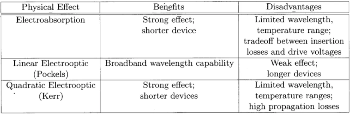
2.1 Summary of the benefits and disadvantages of physical modulation effects . 43
3.1 Refractive indices of materials in the arsenide-based, p-i-n modulator het-erostructure that is designed to operate at A=0.8pm. . . . . 55
3.2 Calculated values of V, at A=0.8pm for Alo.8Gao.2As/Ino.5 3Gao.4 7P
Mach-Zehnder Interferometer-based devices of various lengths oriented in the < 011 > direction, assuming an r41 = 1.44 -10-12 m/V. . . . . . . . . 58
3.3 Material thickness and doping values that were used in simulating the elec-trical behavior of the n-i-n MOS heterostructure. . . . . 72 3.4 Relative permittivities of the AlOY and AlGai_,As materials . . . . 75 3.5 Calculated area-normalized capacitances at low frequency of the Al2OY and
upper cladding layers. . . . . 75 3.6 Refractive indices at A=0.8pim of AlGaiAs materials composing the n-i-n
MOS modulator heterostructure. . . . . 80 3.7 Refractive indices at A=0.8tm of GaAs, AlAs and AlOY materials composing
the n-i-n MOS modulator heterostructure. . . . . 80 3.8 Calculated values of V, at A=0.8[tm for the Al0.17Gao.83As/Alo.27Gao.73As
MOS devices of various Mach-Zehnder arm lengths oriented in the < 011 > direction, assuming an r41 = 1.44 -10-12 m/V. . . . . 84
4.1 Modified NR7-3000P negative photoresist process . . . . 105 4.2 Summary of measured optical power transmission . . . .111 4.3 Summary of the 12pm-wide MMI theoretical calculations for varying
wave-lengths of operation, and calculated for both Adachi and Gehrsitz indices of refraction at these wavelengths . . . . 113
4.4 Summary of the 16pm-wide MMI theoretical calculations for varying wave-lengths of operation, and calculated for both Adachi and Gehrsitz indices of
refraction at these wavelengths . . . . 113
4.5 Modified BCB annealing process . . . . 118
A. 1 Mechanical, electrical, and thermal properties of the Cylotene 3022 series. . 138 B. 1 Oxide chemical vapor deposition process . . . . 147
B.2 Mask 1 -AZ5214 positive photoresist 1.5pm-thick photolithography process 147 B.3 AZ5214 curing/plasma ashing process . . . . 148
B.4 SiO2 RIE process with an AZ5214 protective etch mask . . . . 148
B.5 Removal process of the AZ5214 photoresist following the SiO2 RIE . . . . . 148
B.6 HBr RIE for the removal of the top doped semiconductor layers . . . . 148
B.7 Oxide chemical vapor deposition process for ICP-RIE etch mask . . . . 149
B.8 Mask 2 -NR7-3000P negative photoresist 3pm-thick photolithography process 149 B.9 SiO2 RIE process with an NR7-3000P etch mask . . . . 149
B. 10 NR7-3000P negative photoresist stripping process . . . . 149
B.11 ICP-RIE process for GaAs-based materials . . . . 150
B.12 AlAs oxidation process . . . . 150
B.13 Benzocyclobutene application process . . . . 150
B. 14 Benzocyclobutene furnace anneal process . . . . 150
B. 15 Oxide chemical vapor deposition process for the etch of the Benzocyclobutene to expose the Mach-Zehnder Interferometer arms . . . . 151
B.16 Mask 3 -NR7-3000P negative photoresist 3pum-thick photolithography process 151 B.17 SiO2 RIE process with an NR7-3000P etch mask . . . . 151
B.18 NR7-3000P negative photoresist stripping process . . . . 152
B. 19 Benzocyclobutene RIE etch back with the SiO2 etch mask . . . . 152
B.20 Hydrofluoric dip for removal of SiO2 over the Mach-Zehnder Interferometer arm s . . . . 152
B.21 Mask 4 - NR7-1500PY negative photoresist 1.5pm-thick photolithography process... ... ... .... .. ... .. 152
B.22 Top ohmic contact evaporation . . . . 153
B.24 Bottom ohmic contact evaporation . . . . 153
B.25 Anneal of ohmic contacts . . . . 153
B.26 Oxide chemical vapor deposition process for wet etch mask . . . . 156
B.27 Mask 1 -AZ5214 positive photoresist 1.5tm-thick photolithography process 156 B.28 AZ5214 curing/plasma ashing process . . . . 156
B.29 SiO2 RIE process with an AZ5214 etch mask . . . . 157
B.30 Removal process of the AZ5214 photoresist following SiO2 RIE . . . . 157
B.31 Wet etching procedure for the removal of the top doped semiconductor layers 157 B.32 Oxide chemical vapor deposition process for ICP-RIE etch mask . . . . 157
B.33 Mask 2 - NR7-3000P negative photoresist 3pm-thick photolithography process157 B.34 SiO2 RIE process with an NR7-3000P etch mask . . . . 158
B.35 NR7-3000P negative photoresist stripping process . . . . 158
B.36 ICP-RIE process of GaAs-based materials . . . . 158
B.37 AlAs oxidation process . . . . 158
B.38 Benzocyclobutene application process . . . . 159
B.39 Benzocyclobutene furnace anneal process . . . . 159
B.40 Mask 5 - NR7-3000P negative photoresist 3pim-thick process, facet etch mask 160 B.41 Benzocyclobutene RIE etch back over facets . . . . 160
Chapter 1
Introduction
The emergence of the solid state laser [3] in 1960 marked the onset of research and devel-opment in optical components and devices. Less than two decades later, the optics and communication fields began to overlap as major telecommunication carriers first invested in fiber-optic links at 0.8pm, and later linked continents with transoceanic optical fibers operating at 1.55pim. Today, optical networks continue to thrive due to their bandwidth ca-pability, characteristic high speeds, low losses and cost [4], enabling communication through the encoding of information onto an optical frequency carrier - an integral function known as optical signal modulation.
There are a variety of optical modulator designs, including, but not limited to acousto-optic, electroabsorption, electroacousto-optic, liquid crystal and fiber-optic modulators. Aside from use in telecommunications, optical modulation serves a fundamental function in a wide vari-ety of applications such as optical displays and in measurements. Recently, modulators have found use in optical arbitrary waveform generation (OAWG), a spectral line-by-line pulse shaping technique that produces arbitrary temporal waveforms by phase and amplitude modulation of the spectral lines across an entire bandwidth of a coherent optical frequency comb [5].
The OAWG system, schematically shown in Figure 1-1, is composed of a carrier-envelope phase-stabilized femtosecond oscillator, parallel sets of phase and amplitude modulators, a demultiplexer and multiplexer (often in the form of gratings). The system separates the frequency components of a mode-locked fiber-laser into an optical frequency comb, and employs both broadband phase and amplitude modulators to alter the properties of
CEO-stabilized
Oscillator
Figure 1-1: Schematic of the optical arbitrary waveform generation (OAWG) system. An optical pulse train that is generated by a mode-locked short pulse laser is passed through a demultiplexer in order to decompose its frequency spectrum. A series of modulators ma-nipulate the phase and amplitude of each frequency component, which are then recombined through a multiplexer at the output to create an optical arbitrary waveform.
individual frequency components. Upon multiplexing (recombination) of the modulated spectrum, the system outputs an altered waveform.
Pulse shaping technology that is based on the InP-InGaAsP material system has been re-ported at the telecommunication wavelength [6, 7]. These pulse shaping devices are based on mode-locked laser-compatible fabrication processes that encourage the possibility of full sys-tem integration, but most current OAWG syssys-tems are based on slow reconfigurable elements such as acousto-optic [8] or liquid crystal modulators [9, 10, 11], discrete bulk components that limit performance, stability, scalability and reliability [12). Integrated photonic optical arbitrary waveform generators will provide high-resolution, monolithic, ultra-compact semi-conductor encoder-decoders that support high-speed (> 40 GHz/channel) reconfiguration, scalability and reliability.
The manipulation of broadband frequency combs and the generation of broadband wave-forms is made possible by the parallel processing of spatially separated frequency lines. Such high resolution control of femtosecond elements of the electric field enables several technolo-gies. For instance, the performance of carrier-free ultra-wideband (UWB) wireless devices that are commonly used in imaging, biomedical, and surveillance systems are sensitive to the selection of an impulse signal [13]. Such devices would greatly benefit from the freedom of waveform modulation that is granted with OAWG systems. OAWG is also used in optical
code-division multiple-access (OCDMA) and UWB communication systems at 1.55pm [14], high bandwidth radar and high-speed communication networks, high capacity transmission systems [15, 16], and in generating and processing of high bandwidth RF and optical com-munications signals that require phase and amplitude control [17]. The works of Cundiff et al [18] and Weiner [19] can be consulted for more information on these and additional applications.
1.1
OAWG Based on Ti:Sapphire-Generated Optical Combs
CW~~ DyLRT t4d AG L
REIVOLtJTI
Ix C nter
lioot[
DYE ARG4 Cr YAG
lots~t~t
- 1 - ,Cr -One cycle
To sopphiro Two cyc Its
I 1966 1970 197T 1900 1985 1900 190" 2000 200
ubpetcn YEAR I t
Passive pul~s APM
modeWocking
Figure 1-2: Evolution in laser technologies and developments in the generation of short pulses over the past decades [1].
Figure 1-2 displays the progress over the past decades in the development of ultra-short pulse-generating laser. Significant efforts have been made to shorten the duration of pulses, which has in turn produced broader optical spectrums. Lasers that output pulses on the order of a few femtoseconds, such as the Ti:Sapphire laser, first realized by Moulton [20], have spectrums hundreds of nanometers wide. High resolution optical arbitrary waveform generation necessitates optical frequency combs with repetition rates in the GHz range, that are generated by broadband spectrum optical sources. Stabilized optical combs have been demonstrated using both a Ti:Sapphire and fiber laser sources [21, 22, 23]. At A=1.55pm, optical frequency combs generated by fiber lasers for OAWG applications are pursued due
to the availability of high-speed optical modulators at this wavelength. At A=0.8pm, the stable, optically broadband, carrier-enveloped offset (CEO) locked titanium-doped sapphire laser (Ti:sapphire being the amplifying medium), generates ultrashort, femtosecond pulses ([24]) and hence frequency combs. The high gain of Ti:Sapphire lasers around A=0.8pm encourages exploration of ultra broadband modulators in this wavelength regime for the development of a broadband OAWG system for utilization in communications, research and many more applications that have yet to be envisioned.
1.2
Thesis Organization
Chapter 2 examines the theory behind the physical electroabsorption (EA) and electrooptic (EO) effects that contribute to optical signal modulation. The advantage of the electrooptic effect over electroabsorption due to broadband performance capability is explained, and directional coupler and Mach Zehnder Interferometer (MZI) devices that operate on these effects are introduced. The mathematical theory of both devices is provided to support the adoption of low-power MZI modulators.
Chapter 3 provides an overview of past work in the field and the previously pursued ridge waveguide modulator design that is based on a p-i-n configuration. The design and simulation of optical waveguides and power splitters is explored, and a mask set is offered. The subsequent fabrication process and testing results are presented, motivating the de-velopment of a novel n-i-n, Metal-Oxide-Semiconductor (MOS) epitaxial heterostructure. The electrical performance of the n-i-n MOS modulator is investigated and the fabrication, design benefits and disadvantages of the heterostructure are highlighted.
Chapter 4 introduces a self-aligned mask set that improves upon the former by offering full power transfer between optical components of the waveguide. The mask set is applied to a specialized fabrication process in the pursuit of a novel n-i-n epitaxial heterostructure-based modulator. Measurements and a thorough analysis of the results are reported, and an optimized fabrication process is detailed and verified through the characterization, providing a significant improvement in waveguide operation and optical losses. Additionally, the modeling of power splitting devices is discussed, and the characterization of fabricated multimode interferometers (MMIs) and Y-splitters is presented and compared to theory, verifying the performance of modulator components that are based on the n-i-n structure.
Chapter 5 concludes the thesis with a summary of the work that was accomplished and offers future directions of research in the effort to construct optical modulators operating at A=0.8pm. A second generation mask set design is provided, improvements on the n-i-n heterostructure aimed at achieving push-pull operation, and an alternative electrode configuration for improved electrical operation are discussed.
Chapter 2
Optical Signal Modulation
An optical carrier is described by its physical qualities -polarization, amplitude (Ao), phase
(#),
and frequency (w). The carrier is expressed as a time-varying electric field of the formE(t) = Aocos(wot - 0) = Re[8Aoei0oexp(-iwot)] (2.1)
where E is the electric field, Re represents the real part, 8 denotes a unit vector and the field polarization. Modulation of these elemental optical signal properties (amplitude, phase, frequency, and polarization) is the foundation of optical communication.
The electric field output of a Light Amplification by Stimulated Emission of Radiation device, or laser, is described by the expression in Equation 2.1, and can be either directly modulated or indirectly modified by external modulator devices. Direct modulation of a semiconductor diode laser is a common procedure that is inherently limited by the properties of the diode itself [25] and the current flow through it, resulting in center frequency shifting (chirping - the ratio of the change in refractive index An to the change of the extinction ratio Ak), reduced effective feedback levels, thermal effects and delays [26, 271, and spectral linewidth broadening. These concerns and others that are related to direct modulation present a formidable obstacle to reliable long-haul optical communication systems, limiting transmission speeds and distances [28].
External optical modulators [29] are an alternative to direct modulation, allowing the source to operate independently and improving the accuracy of the frequency control (by eliminating carrier induced frequency variation) and the output power control [30]. Despite the additional 5-7dB of insertion losses [31], external modulators are advantageous due to
their high operational speeds and high extinction ratio, allowing for data rates of up to 50Gb/s [32].
There are several basic types of modulation effects and hence external modulators. This chapter provides an overview of the prevalent electroabsorption and electrooptic effects and offers insight into their application in the construction of optical phase and amplitude modulators.
2.1
Physical Optical Modulation Effects
Materials are characterized by real and imaginary parts, which correspond to the refractive index and absorption coefficient. The refractive index, n, describes the decrease in the phase velocity of light that is traveling through a medium relative to light that is propagating in a vacuum. The absorption coefficient, a, dictates how far light can propagate before it is absorbed by the material. Both the refractive index and the absorption coefficient are wavelength dependent and are related through the Kramers-Kronig relation
n(w) = 2 (W 2 du' (2.2)
where c is the speed of light, w is the frequency of interest, and w' the frequencies over which integration is performed. The relationship clarifies that a modification of the absorption induces a change in the refractive index (or vice versa). Adjustments in the absorption coefficient are associated with amplitude modulation of an optical carrier, while changes in the phase, frequency, and polarization are correlated with the index of refraction.
The two classes of external modulators - absorption and electrooptic - are built upon the Kramers-Kronig relationship. Absorption-based modulators are typically small (on the order of microns in length), and utilize the strong tuning effect of an applied electric field on the absorption edge of quantum wells. Electrooptic modulators (longer devices due to the relatively weaker linear electrooptic coefficient) [28] exploit the electrooptic properties of compound semiconductor structures and their high indices of refraction to produce strong electric fields and efficient index change. While the following sections provide a basic overview of the physical modulation effects that are considered in this work, for completeness, please refer to the discussions in [2].
2.1.1 Absorption Effects
Electroabsorption modulators are key components in optical fiber communication systems. Their main strengths are the possibility of integration with other semiconductor photonic devices such as distributed feedback (DFB) [33] and distributed Bragg reflector (DBR) lasers, low cost [34], low chirp, high speed, and low driving voltages and small device dimensions.
Operation of electroabsorption modulators is based on the Franz-Keldysh effect and the principle that an applied electric field can shift the absorption spectrum and change the amount of light that is absorbed. This type of modulator is implemented with either bulk semiconductors or multiple quantum well (MQW)/quantum dot structures, typically using compound semiconductors. MQW and quantum dot structures apply the quantum-confined Stark effect (QCSE) to achieve a high modulation extinction ratio.
Broadband GaAs/AlxGai_,As modulators spanning wavelengths between 905nm and 960nm have been demonstrated using the Franz-Keldysh effect [35]. Despite this and other reported successes, the Franz-Keldysh effect is weak and is enhanced only by millimeter-scale devices and high driving voltages, relative to the stronger QCSE. Therefore, QCSE is the primary effect that is pursued in the design of modulators. Wood et al have demonstrated P-I-N, GaAs/AlGai .As multiple quantum well (MQW) absorption modulators operating at 860nm [36]. Tobin and Bruno [37] designed a GaAs/AlGaAs triple-quantum-well, P-I-N modulator structure that uses the QCSE for an application operating at 810nm. In this con-figuration, the coupling between multiple wells (composed of either GaAs or Alo.o6Gao.94As
and that are separated by very thin Alo.3Gao.7As layers) allows the photon transition energy
to be tuned to the desired value. Jarrahi et al fabricated velocity-matched, traveling wave Mach-Zehnder modulators at 870nm with multiple AlGai_2As quantum wells on a GaAs substrate. The device displayed a low driving voltage of 0.45V by incorporating both the QCSE and a resulting electro-refractive effect [38].
2.1.2 Linear Electrooptic Effect
The refractive index of a material that experiences a change due to an applied electric field is described by the following power series expansion
A rijkEk + RjkiEkE1 +... (2.3)
where Ek is the kth component of the electric field, rijk is the linear electrooptic coefficient (describing a linear dependence on the applied electric field) and Rik is the quadratic elec-trooptic coefficient. The elecelec-trooptic effect, also known as the Pockels effect, is represented by: / A 1\ Tii T12 r13 n2 1 r 2 2 r2 3 El 1F 1 A2 T31 T32 r3 3 E2 A r4 1 r4 2 r4 3 YZ E3 r5 1 r5 2 r5 3 n., A1 T61 r62 r63
For GaAs, an isotropic cubic crystal with four-fold symmetry of group 43 that lacks inversion symmetry, the electrooptic matrix reduces to
0 0 0 0 0 0 0 0 0 r41 0 0 0 r5 2 0 0 0 r6 3
where r41 = T52 = r63 for isotropic materials. For example, a change, An, that is produced
by a y-directed applied electric field is
1
A x2z= r52E = (2.4)
In a GaAs-based modulator, the applied electric field induces a change in the refractive index along perpendicular axes, i.e. Ey produces a response in the x and z-directed refractive
indices. However, the electric field also distorts the index ellipsoid from a circle in the xz plane to an ellipsoid rotated by 45' off the xz plane. Hence, the applied electric field Ey results in modified n,,' and nz' (the refractive indices in the x' and z' major axes of the index ellipsoid). An incoming beam that is directed along the z axis has a TE component along the x axis and a TM component along the y axis. The TE mode will be affected by the modified n', while the TM mode lying on the same axis as the electric field, will not feel the effects of a An (consequently, the device's efficiency is reduced as only the TE mode of the beam undergoes modulation [39]). An optical wave propagating along the z' axis and polarized in the x' direction will have the following expression for the change in the index of refraction:
1
Ant' =r 41n3EY (2.5)
Alternately, an optical wave propagating along the x' axis and polarized in the z' direction will have a change in the index of refraction similarly determined by
1
Anz' = I r41n3EY (2.6)
2
The linear electrooptic effect further describes the effects of an applied electric field on the phase of an optical carrier. The total phase shift of a beam traveling along the z axis, that is induced by an electric field that is applied along the y axis, is given by
Ap = koLAn = 2Ln 3 r4 E (2.7)
A 2
where k' is a wavevector equal to 2-, L is the modulator length, r41 is the y-axis electrooptic
coefficient (typically on the order of 1-10- 12m/V [30, 40] and varies little with composition and wavelength [41]) and A is the wavelength of operation. The relationship between the applied voltage and the corresponding electric field is expressed as
V = Ey - tg (2.8)
between the applied voltage and the phase shift is given by
7r Lnsr4 1V (2.9)
A tg
The phase shift that is shown in Equation 2.9 is an important concept of optical inter-ference, which is illustrated in Figure 2-1. If the crests (or troughs) of two waves meet at the same time and are superimposed, they will combine constructively to form a wave with a magnitude equal to the sum of the individual amplitudes of the two waves (top image). The principle of constructive interference occurs when the difference in phase between the two waves with the same magnitude is an integer multiple of 27. When the phase difference between the same waves is an odd integer multiple of 7r (i.e., 37r, 57r, etc.), the crest of
one wave will meet the trough of the other wave at the same time. In this scenario, the waves will destructively interfere, and the magnitude of the combined wave will be equal to the difference in amplitude between the two waves (bottom image). In modulators that are based on principles of optical interference, a phase shift of
#
= r between two optical signals of equal magnitude yields signal extinction, and requires an applied voltage known as V, described byV, = A 9 (2.10)
Ln3r4 1
An early example of a modulator that is based on the linear electrooptic, or Pock-els, effect is a double heterostructure GaAs/AlGaiAs design [42] and demonstrated a drive voltage of
1OV
over the 1mm-long device (at A=1.153pm). The Pockels effect is de-scribed as weak in bulk modulators that are composed of III-V materials (i.e. GaAs [40]). Accordingly, these devices require higher applied voltages to achieve signal extinction. In contrast, multiple quantum well (MQW) heterostructures exploit an electrooptic effect with a quadratic dependence on the electric field intensity (i.e. Kerr effect) to construct shorter and lower voltage-length (VL) modulator devices than those created with bulk materials and the corresponding Pockels effect. Despite these benefits, MQW modulators which suffer from higher propagation losses [43] relative to bulk semiconductor devices, typically produce small changes in the refractive index [44], and are limited to narrow operational wavelength and temperature ranges.Wave # Wave # A 0 A
IVLN/27L\A
~AAL2J+
~vv
vv v
t t Wave #1 t Wave #2T-AO-v:v v v V
AA A
V VV
tConstructive Interference at output
t
Destructive Interference at output
t
Figure 2-1: Superposition of waves resulting in constructive or destructive interference. The combination of two waves of equal phase and amplitude, A0, results in constructive
interference at the output (top figure). The combination of two waves of equal amplitude but with a relative phase retardation of 1800 between them yields destructive interference of the signals at the output and complete signal extinction (bottom figure).
A A A A A
V V V V V
2AO
2.2
Amplitude Modulators
Electrically-induced index or absorption changes in guiding materials are the basis of am-plitude modulation. The phase modulation resulting from the varied refractive index is translated into amplitude modulation through devices such as directional couplers and Mach-Zehnder Interferometers that are described in the following sections. For more infor-mation on a variety of modulation devices, please consult the works of Dagli [28], Dakin and Brown [30], and Saleh [45].
2.2.1 Directional Coupler
Directional couplers are the building blocks of both optical waveguide switches and intensity modulators. While this section covers the relevant theory on the operation of directional
couplers as modulators, information on coupled-mode theory is available in [46, 47, 48]. The directional coupler consists of two parallel waveguides (A and B) in close proximity to each other over a length of L, allowing for evanescent coupling to occur between the waveguides. Optical coupling is controlled by two variables:
1. The coupling coefficient ,, which is adjusted by the application of an electric field over the waveguides which instigates a change in the wavelength and waveguide dimensions, as well as in the refractive index of the propagating mode. The coupling coefficient is related to L, the length at which the optical power shifts completely from one waveguide to the other, by
L = 7r/2 (2.11)
2. A3, the mismatch between the propagation constants of both waveguides [45]. The fundamental mode propagation constant, 13, represents the variance in the elec-tromagnetic wave amplitude as it propagates in space, and is defined as the wavenumber multiplied by the refractive index of the waveguide within which it travels, or
= n (2.12)
A0
A#, the propagation mode mismatch which in turn is designated as
A/3 = #1 -3 2 = An 27 (2.13)
WaveguideA
Waveguide B
Figure 2-2: The directional coupler consists of two parallel waveguides (A and B) in close proximity to each other over a length of L, allowing for evanescent coupling to occur between the waveguides.
where
#1
and#2
are the propagation constants corresponding to the two waveguides, andAn
is the difference between their respective indices of refraction. If /3=0 (the waveguides are equivalent physically) and only one of the waveguides is excited at the input so that A(O)=Ai and B(O)=0, the power from waveguide A will transfer fully to B at the coupling length, L.To construct a modulator with a directional coupler, the electrodes are positioned over (and parallel to) the waveguides within the coupling region. The electric field that is produced by an applied voltage changes the refractive index and consequently the coupling ratio. A change in the refractive index, n, in response to a time varying external voltage, v(t), is expressed as
n(t) = no + An = no + Kv(t) (2.14) where K is a proportionality constant set by the geometry, the physical effect and the material. Under external perturbation, the effect on the refractive index as described in Equation 2.14 combines with the expression for the propagation constant in Equation 2.12 to produce a
#1
and#2
of#2 = n2(t) = #0 + #2 = r(no + K2V(t)) (2.16)
Ao Ao
The power transfer between the two waveguide is expressed as the ratio, T:
T = PBz = (- 2sinc2
[
(I + )2) (2.17)PA(z = 0) 2) 27r
The transfer function is not periodic, and has a maximum for
A/3L
= 0 and a null for A3L v/57r. To switch the modulator from the on state to the off state, a switching voltage, or V, is applied. The directional coupler is most often implemented as a switch device, but has also been employed in unison with physical effects to produce intensity modulators. For in-stance, Khan et al designed an electrooptic directional coupler modulator at A=0.8pbm with propagation losses of 3.4dB/cm [49]. The 3.5mm-long AlGai-xAs/GaAs ridge waveguide modulator had a corresponding drive voltage of 2V. The ridge design confined the optical mode, allowing a high overlap between the optical and electrical modes and reducing the required applied voltage.2.2.2 Mach-Zehnder Interferometer
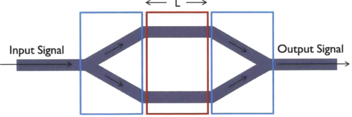
Interferometric devices apply the principle of interference to perform relative measurements. The Mach-Zehnder Interferometer (MZI), that was developed by Ludwig Mach and Ludwig Zehnder, measures the relative phase shift between two optical signals propagating within its two arms [50, 51]. In the MZI, which is shown in Figure 2-3, an input optical wave from
:
L
>Input Signal
Output Signal
Figure 2-3: The MZI structure is composed of input and output waveguides, Y-junctions (within blue boundary) that split and recombine optical power, and Interferometer arms (within red boundary) of length L.
a coherent optical source is divided equally into two paths (in this case, using a Y-junction device). The split wave propagates through the arms of the interferometer and recombines at a second junction at the opposite end of the arms. At the output of the second Y-junction, the recombined wave - a result of interference -is coupled into a waveguide through
which the beam propagates to the device output.
Ideally, the power split to each arm at the Y-junction is equal to half the original power, and is expressed as the power splitting ratio, s2. However, device processing is often inaccurate and results in uneven pathways. The resulting formula for s2 includes a factor of
(
that considers fabrication errors that may affect the power split:1
S2
= - + (2.18)
2
The interferometer arms of the MZI are independent phase modulators of length L, each with propagation constants (13, and /32) associated with their propagating modes, and phase shifts (oi and W2) that are in response to the applied electric field. The result of the
recombination of phase modulated optical waves is an output signal that has its amplitude modulated relative to the input.
There are two states for the MZI modulator -on and off. When the interferometer arms and the paths traversed by the split optical beams are identical, that is,
#1L = #2L (2.19)
there is constructive interference at the modulator output. As exhibited in Figure 2-4(a), when no voltage is applied to either of the arms, a system that had a single mode signal as the input will similarly output a single mode. However, if the voltage equivalent to V, is applied to one of the interferometer arms [see Figure 2-4(b)], the phase of the optical signal will shift 1800 relative to the phase of the signal propagating in the other arm, such that
(#1 - #2)L = 7r (2.20)
At the output, the signals recombine and interfere destructively. As the two beams interfere along the length of the output waveguide, a higher mode with a null in the center is excited. This mode radiates out if the waveguide is single mode, and only if the path is long enough
V=o
Input output
(a)
V=V I
Input 1800 phase shift Output
(b)
Figure 2-4: The Mach-Zehnder Interferometer (MZI) modulator at the on (a) and off (b) states. For a single mode launched into the modulator input - (a) If no voltage is applied along either arm of the interferometer, there is no difference in phase between the divided optical signals traveling along each arm, and the output signal is a fundamental mode. (b) If a voltage equivalent to V, is applied to one of the arms, the signal is phase shifted 1800
relative to the other arm and the carriers interfere destructively. If the waveguides support higher order modes, the fundamental mode will be converted to higher order modes at the output.
for the mode to completely radiate away. If the waveguide is not sufficiently long, there will be power present at the output. If the waveguide is not single mode, the fundamental
mode will be converted to higher order modes at the output [30].
is generally defined as
A(z) = AOe-jz (2.21)
The amplitude at the MZI output (A,) is expressed relative to the optical amplitude at the input (Ai) of the MZI as
A, = Aj[s2e-j(/1L+2(pi) + (1 - s2)e-j(#2L+202)] (2.22)
Setting s2 to its value from Equation 2.18, the output amplitude can be further developed into [30]
A, = Aj[cos(-) - 2j~sin(y)]e- 2(wi±p2 (2.23)
where -y is equal to
7 ( 31 /2 ) 3 +(i (L 2) (2.24)
If the pathways are equal such that there is no phase shift between the interferometer arms and the fabrication is ideal (yielding a one-half power split) then Equations 2.15, 2.16, 2.23, and 2.24 simplify to
Ao = Aicos (- *(K 1 - K2)LV(t) (2.25)
\(AO
and can be further expressed as a transfer function
A 2 =cos2 (K1 - K2)LV(t)) (2.26)
In contrast with the directional coupler modulator, the transfer function of the Mach-Zehnder interferometer modulator is periodic. The voltage that is applied to switch the modulator from the on state to the off state, Vr (explained in Section 2.1.2), is
Ao

![Figure 1-2: Evolution in laser technologies and developments in the generation of short pulses over the past decades [1].](https://thumb-eu.123doks.com/thumbv2/123doknet/14185431.477029/25.918.277.659.382.673/figure-evolution-laser-technologies-developments-generation-pulses-decades.webp)
![Figure 3-1: Common semiconductor materials in the III-V group and associated bandgap energies, lattice constants and emission wavelengths [55]](https://thumb-eu.123doks.com/thumbv2/123doknet/14185431.477029/49.918.216.737.106.471/figure-semiconductor-materials-associated-energies-constants-emission-wavelengths.webp)