HAL Id: hal-00394779
https://hal.archives-ouvertes.fr/hal-00394779
Submitted on 16 Oct 2013
HAL is a multi-disciplinary open access
archive for the deposit and dissemination of sci-entific research documents, whether they are pub-lished or not. The documents may come from teaching and research institutions in France or abroad, or from public or private research centers.
L’archive ouverte pluridisciplinaire HAL, est destinée au dépôt et à la diffusion de documents scientifiques de niveau recherche, publiés ou non, émanant des établissements d’enseignement et de recherche français ou étrangers, des laboratoires publics ou privés.
Ultra-high Q/V Fabry-Perot microcavity on SOI
substrate
Philippe Velha, E. Picard, T. Charvolin, E. Hadji, Jean-Claude Rodier,
Philippe Lalanne, David Peyrade
To cite this version:
Philippe Velha, E. Picard, T. Charvolin, E. Hadji, Jean-Claude Rodier, et al.. Ultra-high Q/V Fabry-Perot microcavity on SOI substrate. Optics Express, Optical Society of America - OSA Publishing, 2007, 15 (24), pp.16090-16096. �hal-00394779�
Ultra-High Q/V Fabry-Perot microcavity
on SOI substrate
P. Velha1,2,3, E. Picard1, T. Charvolin1, E. Hadji1, J. C. Rodier2, P. Lalanne2 and D. Peyrade3,*
1 Département de Recherche Fondamentale sur la Matière Condensée, CEA,
17 rue des Martyrs, -38054 GRENOBLE Cedex 9, France.
2 Laboratoire Charles Fabry de l’Institut d’Optique, CNRS,
F-91403 ORSAY Cedex, France.
3 Laboratoire des Technologies de la Microélectronique, CNRS,
17 rue des Martyrs, F-38054 GRENOBLE Cedex 9, France. *Corresponding author: [email protected]
Abstract: We experimentally demonstrate an ultra high Q/V nanocavity on
SOI substrate. The design is based on modal adaptation within the cavity and allows to measure a quality factor of 58.000 for a modal volume of 0.6(λ/n)3 . This record Q/V value of 105 achieved for a structure standing on a physical substrate, rather than on membrane, is in very good agreement with theoretical predictions also shown. Based on these experimental results, we show that further refinements of the cavity design could lead to Q/V ratios close to 106.
2007 Optical Society of America
OCIS codes: (130.0130) Integrated optics; (130.7408) Wavelength filtering devices; (250.5300)
Photonic integrated circuits; (230.5298) Photonic crystals;
References and links
1. J. Poon, L. Zhu, G. DeRose, and A. Yariv, “Transmission and group delay of microring coupled-resonator optical waveguides,” Opt. Lett. 31, 456 (2006)
2. A. Melloni and M. Martinelli, “Synthesis of Direct-Coupled-Resonators Bandpass Filters for WDM Systems,” J. Lightwave Technol. 20, 296 (2002)
3. Bradley Schmidt, Qianfan Xu, Jagat Shakya, Sasikanth Manipatruni, and Michal Lipson, “Compact electro-optic modulator on silicon-on-insulator substrates using cavities with ultra-small modal volumes,” Opt. Express 15, 3140 (2007), http://www.opticsinfobase.org/abstract.cfm?URI=oe-15-6-3140
4. K. Sakoda, ”Optical Properties of Photonic Crystals,” Springer (2004)
5. O. Painter, R. K. Lee, A. Scherer, A. Yariv, J. D. O. Brien, P. D. Dapkus, I. Kim, “Two-Dimensional Photonic Band-Gap Defect Mode Laser,” Science 84, 1819 (1999)
6. D. K. Armani, T. J. Kippenberg, S. M. Spillane & K. J. Vahala, “Ultralow-threshold microcavity Raman laser on a microelectronic chip,” Nature 421, 925 (2003)
7. T. Tanabe, M. Notomi, E. Kuramochi, A. Shinya and H. Taniyama, “Trapping and delaying photons for one nanosecond in an ultrasmall high-Q photonic-crystal nanocavity,” Nature Photonics 1, 49 (2007) 8. S. Noda, M. Fujita and T. Asano, “Spontaneous-emission control by photonic crystals and nanocavities”
Nature Photonics 1, 449 (2007)
9. M. W. Pruessner, T. H. Stievater, and W. S. Rabinovich, ” Integrated waveguide Fabry-Perot microcavities with silicon/air Bragg mirrors,” Opt. Lett. 32, 533 (2007)
10. Y. Tanaka, T. Asano, R. Hatsuta, and S. Noda, “Investigation of point-defect cavity formed in two-dimensional photonic crystal slab with one-sided dielectric cladding,” Appl. Phys. Lett. 88, 011112 (2006) 11. J. S. Foresi, P. R. Villeneuve, J. Ferrera, E. R. Thoen, G. Steinmeyer, S. Fan, J. D. Joannopoulos, L. C.
Kimerling, Henry I. Smith & E. P. Ippen, “Photonic-bandgap microcavities in optical waveguides,” Nature
390, 143 (1997)
12. D. Peyrade, E. Silberstein, Ph. Lalanne, A. Talneau, and Y. Chen, "Short Bragg mirrors with adiabatic modal conversion," Appl. Phys. Lett. 81, 829 (2002)
13. P. Velha, J. C. Rodier, P. Lalanne, J. P. Hugonin, D. Peyrade, E. Picard, T. Charvolin, E. Hadji, “Ultracompact silicon-on-insulator ridge-waveguide mirrors with high reflectance,” Appl. Phys. Lett. 84, 171121 (2006)
14. C. Sauvan, G. Lecamp, P. Lalanne and J.P. Hugonin, “Modal-reflectivity enhancement by geometry tuning in Photonic Crystal microcavities,” Opt. Express. 13, 245 (2005),
http://www.opticsinfobase.org/abstract.cfm?URI=oe-13-1-245
#86247 - $15.00 USD Received 8 Aug 2007; revised 11 Oct 2007; accepted 14 Oct 2007; published 20 Nov 2007 (C) 2007 OSA 26 November 2007 / Vol. 15, No. 24 / OPTICS EXPRESS 16090
15. P Velha, J C Rodier, P Lalanne, J P Hugonin, D Peyrade, E Picard, T Charvolin and E Hadji, “Ultra-high-reflectivity photonic-bandgap mirrors in a ridge SOI waveguide,” New Journal of Physics 8, 204 (2006) 16. P. Yeh, “Optical Waves in Layered Media,” Wiley-Interscience (1988)
17. E. Silberstein, P. Lalanne, J. P. Hugonin, and Q. Cao, "Use of grating theories in integrated optics," J. Opt. Soc. Am. A 18, 2865-2875 (2001)
18. G. Lecamp, J.P. Hugonin and P. Lalanne, "Theoretical and computational concepts for periodic optical waveguides," Opt. Express 15, 11042-60 (2007).
19. H. Kim, I.M. Lee and B. Lee, "Extended scattering-matrix method for efficient full parallel implementation of rigorous coupled-wave analysis," J. Opt. Soc. Am. A 24, 2313-2327 (2007).
1. Introduction
In recent years, the race for faster optical communications and data processing has motivated research towards optoelectronic devices. The latter will need more functional elements directly interconnected on a single chip to create truly integrated circuits. Functional devices such as channel drop filtering [1,2], On-Off switch or light modulator [3] can be imagined. It is admitted [4] that the exaltation of optical non-linearity and spontaneous emission inhibition or exaltation (threshold laser reduction) [5] are mainly governed by the Q/V ratio. Thus, high quality factor (Q) optical micro-cavities that confine light in small modal volumes (V) at optical wavelength scales are essential components for signal processing. Highest Q as large as 108 were obtained on silica toroïds [6]. But these toroïds have a huge modal volume and gives a Q/V of approximately 5. 104 (λ/n)3. Recently, the interest in manufacturing ultra small micro-cavities with extremely high Q/V in two dimensional PC slabs have been boosted as those cavities offer mode volumes close to the theoretical limit of V= (λ/2n)3. Q factors as high as 106 [7,8] have been achieved. These resonators are Fabry-Perot cavities where the Bloch mode is bouncing between two mirrors fabricated on semiconductor air membranes. Even though suspended membranes are viable at a research level, several issues cloud such cavities: they present many drawbacks in terms of electrical injection, thermal dilatation and mechanical stability. So, an ultra-small high Q cavities realized on a substrate is a critical milestone [9-12].
In this work, we report on high-Q, small-V linear Fabry-Perot micro-cavities manufactured in ridge waveguides on silicon-on-insulator wafers without removing the silica cladding. First, we briefly describe the design of modal adaptation principle and present the fabrication process of the photonic nanostructure. After describing the characterization set-up, we detail the optical properties of the microcavities in terms of Q factor, transmittance and losses. Finally, we discuss the increase of cavities performances with the help of a predictive model.
2. Design and fabrication of Fabry-Perot microcavities
In 1997, Foresi et al. [11] demonstrate the viability of a cavity design consisting in two mirrors made of a chain of periodic holes located on a ridge waveguide. Until recent works, the Q factors of such cavities stayed very low and did not exceed 500. The introduction of a tapered section based on modal adaptation permitted to enhance Q factor [12] and we demonstrated the possibility to reach Q factor of about 9000 in a previous work [13]. The tapering process is based on Bloch mode engineering concepts [14] and consists in the adaptation of modes profiles between the fundamental cavity mode supported by the ridge waveguide and the evanescent Bloch mode of the periodic mirror. The design takes into account the vertical cladding dissymmetry of the structure where the cavity lies on the silica cladding. It results in the addition of a tapered section of four holes placed next to the periodic section of the mirror composed of N holes, see Fig. 1. Simulations of such a design show that radiation losses at the ridge-mirror are divided by 400 and that the Q value of the resonant peak calculated for an infinite number of holes is as high as 400,000. This tapering design increase the cavity performance (Q is multiplied by 800) in comparison to a classical Fabry-Perot device with fully-periodic mirrors [15].
#86247 - $15.00 USD Received 8 Aug 2007; revised 11 Oct 2007; accepted 14 Oct 2007; published 20 Nov 2007 (C) 2007 OSA 26 November 2007 / Vol. 15, No. 24 / OPTICS EXPRESS 16091
Silicon-On-Insulator wafers used in this work were manufactured by SOITEC. Stack layer consists of a 340 nm silicon top layer (waveguide core) and a 2 µm thick SiO2 insulator
supported by a bulk silicon substrate. The ridge waveguide (500 nm width) and holes patterning is performed by electron-beam lithography with a Leica VB-6UHR on a single 400 nm thick NEB22 negative resist spin coated on top of the sample. The electron beam energy is 100 keV resulting in a 5-nm probe-beam diameter. After developing the resist, Inductive-Coupled-Plasma etching of the sample is performed in an industrial plasma chamber (DPS from Applied Materials Inc).
The native oxide is first removed by a short breakthrough with a CF4 gas mixture. Then, the silicon native layer is etched with a HBr, Cl2, O2 gas mixture, at a pressure of 4 mT.
Finally, the resist is stripped by oxygen plasma. Then, each sample is manually cleaved in order to obtain optical facets. As an example, Fig. 1 presents a fabricated Fabry-Perot cavity where each mirror is composed of two sections. The periodic section of the mirror is formed of holes with identical diameter and with identication hole-separation distances. The tapered section is formed with four holes with different diameters and with periods decreasing as one approaches the cavity defect.
3. Optical resonance properties of the microcavities
After cleaving optical facets, the device is mounted on a XYZ translational stage regulated in temperature. TE-polarized light from a tunable laser source emitting from 1.45µm to 1.59 µm is launched into the 9 mm long ridge access waveguide. Light is injected through the cleaved facets in waveguides. We use a polarization maintaining optical fibber. This optical fibber is chemically etched in order to obtain an end diameter of about 2 µm. After passing through the device, the light is collected by a x15 reflective objective. The waveguide output is then imaged, either onto an IR camera for observing light at the output of the cleaved facet, or onto an InGaAs photodiode for transmission measurements. Additionally, when using the photodiode, the imaging system incorporates a diaphragm and a polarizer in order to spatially filter inevitable spurious substrate-guided light. Sample is observed by a microscope with an angle of collection of 30°, which permits to collect the light escaping vertically from the structure. This light is guided via an optical fibber from the microscope objective onto another InGaAs detector.
cavity periodic
mirror taper periodic
mirror taper
1µm cavity
periodic
mirror taper periodic
mirror taper
cavity periodic
mirror taper periodic
mirror taper
1µm
Fig.1. SEM picture of the lineic Fabry-Perot cavity inserted in the silicon waveguide. On both sides of the cavity, each mirror is composed of a taper and of a periodic section. The taper is located on the cavity side of the mirror and is made of four holes with increasing diameter (130, 170, 200, 200 nm) and separated by increasing distances (300, 320, 350 nm respectively). The periodic mirror is made of N holes (N=4 on the picture) with a diameter of 200 nm and a period of 370 nm. The inset presents a magnification of the tapered zone.
#86247 - $15.00 USD Received 8 Aug 2007; revised 11 Oct 2007; accepted 14 Oct 2007; published 20 Nov 2007 (C) 2007 OSA 26 November 2007 / Vol. 15, No. 24 / OPTICS EXPRESS 16092
Figure 2 presents the cavity-loss spectrum of the cavity with N=7. On the whole measurement range, the cavity exhibits a band gap with a sharp resonance at wavelength of 1574 nm. Fabry-Perot oscillations corresponding to the sample facets superimpose on the cavity mode signal and perturb cavity quality factor measurement. In order to separate both contributions, we acquire spectra at different temperature (see the two insets in Fig. 2). In the worst case, this effect could boost the estimation of the cavity Q, concluding to the observation of a Q factor as high as 80 000 (T=21°C). The left-inset (T=20°C) shows a width of the lorentzian peak of 27 pm, which correspond to a Q factor of 58000 in the less favorable case. Many measurements have been performed to estimate the Q value by varying the temperature, and we conclude that the Q is actually larger than 58000. Because the calculated modal volume is approximativly equal to 0.6(λ/n)3 , we estimate that the Q/V ratio is as high as 1.0 105(λ/n)3.
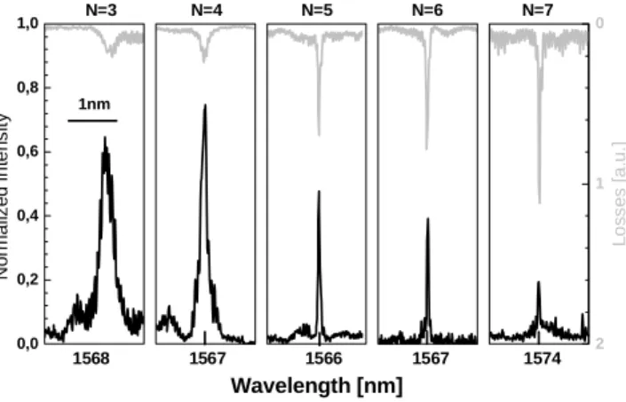
We have also performed measurements for other cavities for N ranging from N=3 to N=7. The spectra in Fig. 3 show the transmission of these cavities in black and the radiation losses measured by the top of the cavity in light grey. Transmission spectra through the device are normalized by a reference waveguide measurement. Spectra collected above the cavity show a resonant peak with the same spectral position and linewidth as observed in transmission spectra. This is consistent with the Fabry-Perot model [16] and gives a second check for the estimation of the Q factor.
1560 1565 1570 1575 1573.9 1574.0 1574.1 T = 20 °C T = 21 °C 27 pm In te n s it y [ u .a ] Wavelength [nm] 1574,0 1574,1 1574,2
Fig. 2. Resonant cavity peak collected above the cavity. The insert details the resonant peak for two regulated temperature of the sample. Left-inset is fitted with a lorentzian curve replicated with a dashed line in the right-inset.
2 1 0 0,0 0,2 0,4 0,6 0,8 1,0 N o rm a liz ed i n te ns it y 1568 1567 1566 1567 1574 Wavelength [nm] N=3 N=4 N=5 N=6 N=7 L o s s e s [a .u .] 1nm
Fig. 3. Evolution of the resonant peak with increasing the number of holes in the periodic mirror (N). The black curve presents the normalized transmission across the cavities, the grey one shows the vertical losses collected by the top of the sample in arbitrary units with inverted axis.
#86247 - $15.00 USD Received 8 Aug 2007; revised 11 Oct 2007; accepted 14 Oct 2007; published 20 Nov 2007 (C) 2007 OSA 26 November 2007 / Vol. 15, No. 24 / OPTICS EXPRESS 16093
As the number N of holes increases, the transmission peak (Tmax) at resonance shows a
global significant decrease, meanwhile losses collected above the cavity increase (Fig. 3 and table 1). When the light is bouncing inside the cavity, it could experience two kinds of losses: In one hand, losses at each reflection due to the mode-profile mismatch and located at the tapered sections. This term is roughly constant and independent of the number of holes in the periodic section of the mirror. In a less significant way, the second source of loss corresponds to in-line losses due to the ridge waveguide roughness estimated to 6 dB/cm.
As the Q factors increase, both the number of reflections inside the cavity and the light path increase. This explains the decrease of Tmax and the increase of the light collected above
the cavity.
Table 1. Experimental Cavity Q’s and Tmax for N ranging from 3 to 7 designed with the same tapering section.
N λr(nm) Qexp Tmax(+/-0.05) 3 1568.22 2,700 0.6 4 1567.26 8,200 0.7 5 1569.09 19,000 0.5 6 1567.62 45,000 0.4 7 1574.00 58,000 0.2 4. Cavity performances
The experimental evolution of the Q factor with the number of holes N is represented in Fig. 4 with black dots and is compared with computational data obtained with a 3D fully vectorial Fourier modal method.
The 3D frequency-domain modal method used in this work for the computation is described in Ref.[17-18]. In brief, the method relies on an analytical integration of Maxwell’s equations along the ridge-waveguide z-axis and on a supercell approach in the two others. Periodic boundary conditions with Perfectly-Matched-Layers implemented as nonlinear coordinate transforms are used in the orthogonal directions to carefully handle out-of-plane far-field radiations in the air and in the SiO2 substrate. Since these layers absorb
non-evanescent radiations, the electromagnetic fields are null on the boundaries of the supercell and are thus periodic functions of the z-coordinates. This allows to calculate the radiated and guided modes in a Fourier basis in each layer (the cylindrical bumps are discretized in a series of thin uniform layers) and to analytically integrate Maxwell’s equations in the z-direction by relating recursively the modes amplitudes in the different layers using a scattering matrix approach [19]. The Q factors in Fig. 4 are computed by looking for the complex-poles
λ
~
of the scattering matrix and by use of the relationQ
=
Re
( )
λ
~
2
Im
( )
λ
~
. In Fig. 5, in order to strongly reduce the computational loads, the Q’s are estimated by calculating the mirror modal reflectivity spectra [18]. From these values, we infer the cavity Q factors using a Fabry-Perot model. The latter has been shown to provide highly accurate predictions for Q for these cavities, see Ref. [13,14]. Convergence tests have been performed to estimate the accuracy of the computational results by increasing the number P of plane-waves retained for the computation. Stable results for the modal-reflectivity and for the Q values have been obtained for P>1000, letting us expect a relative error below 1% for all calculated data. Thus the only approximation results from the spatial discretization (staircase profile) used to numerically encode the mirror holes.Figure 4 shows that the Q factors (model and experimental) augment with N, which corresponds to the increase of the mirror reflectivity.
#86247 - $15.00 USD Received 8 Aug 2007; revised 11 Oct 2007; accepted 14 Oct 2007; published 20 Nov 2007 (C) 2007 OSA 26 November 2007 / Vol. 15, No. 24 / OPTICS EXPRESS 16094
3 4 5 6 7 8 9 10 103 104 105 106 Q f act or
Number of holes in the mirror
Fig. 4. Experimental (dots) evolution of the Q factor for the lineic Fabry-Perot cavity with increasing N. The shaded region represents the theoretical values for an increasing number of holes in the periodic mirror of the cavity and for a tolerance of +/- 10 nm on the nominal value of the hole diameters. The dot curve shows the optimum Q factor value calculated for an optimal cavity length for each N.
The miror (periodic section with N holes + tapered section) is defined by three intrinsic parameters: its modal reflectivity Rm, its modal transmittance Tm and its losses Lm, all linked
by the relation Rm+Tm+Lm=1. The losses Lm correspond to the mode profile mismatch at the
taper and do not depend on N as already mentioned. Both experimental and calculated values saturate as N increase over 4-5 due to the losses located at the tapered section. The experimental Q factor values (dots) are included between two fitted models (grey zone) corresponding to a variation in the nominal hole dimensions of +/-10 nm. It shows the robustness of the cavities performances in association with realistic nanofabrication possibilities.
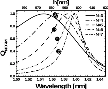
Fig. 5. Evolution of the normalized quality factor QNORM as a function of the resonant
wavelength of for N=3 to N=7. The labeled numbers represent the experimental values (Qexp ,λr). h is the cavity length given by the relation h=λ/neff.
560 570 580 590 600 610 620 1.50 1.52 1.54 1.56 1.58 1.60 1.62 1.64 0.0 0.2 0.4 0.6 0.8 1.0 3 4 5 6 N=3 N=4 N=5 N=6 N=7
Q
NORMWavelength [nm]
7 7 7 7h[nm]
#86247 - $15.00 USD Received 8 Aug 2007; revised 11 Oct 2007; accepted 14 Oct 2007; published 20 Nov 2007 (C) 2007 OSA 26 November 2007 / Vol. 15, No. 24 / OPTICS EXPRESS 16095
Figure 5 details the evolution of calculated QNORM factor (QNORM being the normalised Q
factor obtained by dividing the actual Q by the maximum Q achievable with the same number N of holes) as a function of the cavity defect length h. On the same picture, the experimental values for the resonant wavelengths and Q factors have been added for N ranging from 3 to 7.
We first observe that the calculated QNORM optimum (curves in Fig. 5) is shifting and is
getting sharper as N increases. This shift is due to the fact that the Q factors for N<4 are mainly limited by the mirror transmission Tm , which is minimal for λ=1.55 µm. For N>4, the
Q factor is limited by the losses Lm, which is minimal for λ=1,6 µm. Thus the maximum of Q
factor achievable is shifted from 1,55 µm to 1,6 µm. Secondly, cavities have been designed and fabricated with a constant length h for all N's. The experimental cavity length allows to obtain Q factors close to the optimum QNORM for N=3 and N=4, but a progressively-increasing
wavelength shift is obtained for larger N values. Finally, we report on Fig. 4 (dash-line) the theoretical evolution of Q factor calculated with the optimum h value for every N. Figure 5 additionally shows that the experimental Q factors can be further improved by adjusting the cavity length for each N values in order to have the optimal Q factor.
To conclude, with such a design optimization, cavity Q factor’s could become closer and closer to the calculated value Q=150,000 for N=7 or Q=400,000 for N=10. Moreover, we note that the cavity geometry allows to achieve ultra-high Q/V on a SOI substrate over a broad spectral range (e.g. Q > 58 000 over ~40 nm and Q > 20 000 over ~100 nm).
5. Conclusion
We report on experimental studies of Fabry-Perot microcavities with a tapered sections lying on a substrate. Cavity optical characteristics have been studied for an increasing number of holes in the mirror. This study shows the reliability of the modal adaptation concept and points the fact that large Q factor can be achieved over a wide spectral range of operation (compatible with U-DWDM) and thus could still be improved by adjusting the cavity defect length as a function of the number of holes in the mirrors. Q factor of 58000 with a modal volume of about 0.6(λ/n)3 have been demonstrated. This implies a Q/V of 1.0 105 (λ/n)3 which is, to our knowledge, the highest Q/V value measured on a SOI substrate at telecom wavelengths.
Acknowledgments
This work is supported by the French national program PNANO from the “Agence Nationale de la Recherche” under the MIRAMAN contract and P. Velha benefit from a BDI-CNRS-CEA fellowship. BDI-CNRS-CEA-LETI is acknowledged for providing us with an access to the micro/nanofabrication facility center.
#86247 - $15.00 USD Received 8 Aug 2007; revised 11 Oct 2007; accepted 14 Oct 2007; published 20 Nov 2007 (C) 2007 OSA 26 November 2007 / Vol. 15, No. 24 / OPTICS EXPRESS 16096