HAL Id: hal-02120550
https://hal.archives-ouvertes.fr/hal-02120550
Submitted on 6 May 2019
HAL is a multi-disciplinary open access
archive for the deposit and dissemination of
sci-entific research documents, whether they are
pub-lished or not. The documents may come from
teaching and research institutions in France or
abroad, or from public or private research centers.
L’archive ouverte pluridisciplinaire HAL, est
destinée au dépôt et à la diffusion de documents
scientifiques de niveau recherche, publiés ou non,
émanant des établissements d’enseignement et de
recherche français ou étrangers, des laboratoires
publics ou privés.
Maximization of the open circuit voltage for
hydrogenated amorphous silicon n–i–p solar cells by
incorporation of protocrystalline silicon p -type layers
R. Koval, Chi Chen, G. Ferreira, A. Ferlauto, J. Pearce, P. Rovira, C Wronski,
R. Collins
To cite this version:
R. Koval, Chi Chen, G. Ferreira, A. Ferlauto, J. Pearce, et al.. Maximization of the open circuit voltage
for hydrogenated amorphous silicon n–i–p solar cells by incorporation of protocrystalline silicon p
-type layers. Applied Physics Letters, American Institute of Physics, 2002, 81 (7), pp.1258-1260.
�10.1063/1.1499735�. �hal-02120550�
Maximization of the open circuit voltage for hydrogenated amorphous
silicon
n
–
i
–
p
solar cells by incorporation of protocrystalline silicon
p
-type layers
R. J. Koval, Chi Chen, G. M. Ferreira, A. S. Ferlauto, J. M. Pearce, P. I. Rovira, C. R. Wronski, and R. W. Collinsa)
Center for Thin Film Devices, Department of Electrical Engineering, and Materials Research Institute, The Pennsylvania State University, University Park, Pennsylvania 16802
共Received 11 April 2002; accepted for publication 17 June 2002兲
In studies of hydrogenated amorphous silicon (a-Si:H) n – i – p solar cells fabricated by rf plasma-enhanced chemical vapor deposition 共PECVD兲, we have found that the maximum open circuit voltage (Voc) is obtained by incorporating p-type doped Si:H layers that are protocrystalline
in nature. Specifically, these optimum p layers are prepared by PECVD in the a-Si:H growth regime using the maximum hydrogen-to-silane flow ratio possible without crossing the thickness-dependent transition into the mixed-phase (amorphous⫹microcrystalline) growth regime for the ⬃200 Å p-layer thickness. The strong dependence of the p-layer phase and solar cell Vocon the underlying
i-layer phase also confirms the protocrystalline nature of the optimum Si:H p layer. © 2002 American Institute of Physics. 关DOI: 10.1063/1.1499735兴
High open circuit voltages (Voc) and record high
effi-ciencies for hydrogenated amorphous silicon (a-Si:H) n – i – p solar cells fabricated by rf plasma-enhanced chemi-cal vapor deposition共PECVD兲 have been achieved by incor-porating p-type doped Si:H layers deposited at low tempera-ture (T⬃200 °C) using high hydrogen-to-silane flow ratios
共typically R⬅关H2兴/关SiH4兴⬃50– 200兲.1–3 It was proposed
that such optimum p layers are, in fact, microcrystalline Si:H (c-Si:H) and that this material yields improved cell perfor-mance through an increase in the built-in potential of the junction and through decreases in series resistance and ab-sorption losses.
In Ref. 1, the high conductivities characteristic of c-Si:H were measured only on thick p layers共⬎1000 Å兲; however, the layers incorporated into the devices were much thinner 共⬃100 Å兲. In subsequent studies, the Vocvalues
ob-tained with p layers prepared by PECVD at high R were found to increase further as the p-layer deposition tempera-ture 共T兲 was decreased.2,3 To explain this behavior, an in-crease in p-layer crystallinity with decreasing T was hypoth-esized, yet just the opposite trend for T⬍400 °C had been described earlier for four different sets of PECVD films.4 Reflection high energy electron diffraction 共RHEED兲 pat-terns were also presented as evidence that the optimum p layers werec-Si:H.3RHEED is a highly surface-sensitive technique, however, and so fails to probe the p-layer material closest to the i/ p junction.
In view of these considerations, an explanation of the high Vocvalues of Refs. 1–3 in terms of ac-Si:H p layer is
not compelling owing to a possible barrier for microcrystal nucleation on an amorphous i-layer surface.5–7As a result, 100–200-Å-thick p layers prepared on i layers under certain conditions may be amorphous even at R values as high as 200.8In the present study, the problem of Si:H p-layer
opti-mization has been reconsidered. Light and dark current– voltage characteristics dominated by bulk recombination for state-of-the-art a-Si:H n – i – p solar cells9 have been corre-lated with spectroscopic ellipsometry共SE兲 results for the cor-responding p layers of the n – i – p structures.
Three experimental approaches were applied for p-layer optimization in a-Si:H solar cells.
共1兲 Si:H p layers for use in p – i – n solar cells were
devel-oped for high nucleation density and single-phase micro-crystalline structure in 100-Å-thick films on glass/ZnO and glass/SnO2/ZnO substrates using a single-chamber
rf PECVD system and guidance from real time SE
共RTSE兲. In this approach, p-layer gas mixtures of 关H2兴/关SiH4兴/关B(CH3)3兴 were used, and a deposition
phase diagram revealed the preferred conditions of R
⫽200 and D⫽关B(CH3)3兴/关SiH4兴⫽0.02 for immediate
high-densityc-Si:H nucleation on ZnO.10The p – i – n cell structures incorporated an R⫽0 i layer to avoid pos-sible p-layer substrate-induced microcrystallinity.7
共2兲 Si:H p layers for use in n – i – p cells were developed in
a similar manner as the p layers for p – i – n cells. In this approach, however, the underlying i-layer surface was subjected to a 2 min H2-plasma treatment that generates
nanocrystalline Si:H nucleation sites for the p-layer deposition. A wide window for single-phase c-Si:H was found using 关H2兴/关SiH4兴/关BF3兴 mixtures with D
⫽关BF3兴/关SiH4兴⫽0.2 and R⫽200. 8
This preferred p-layer process was then adopted for n – i – p cells on Cr-coated glass using an R⫽10 i layer.
共3兲 After fabrication of p – i – n and n – i – p solar cells with
p layers designed for dense, single-phasec-Si:H struc-ture, a number of state-of-the-art n – i – p devices were fabricated on Cr-coated glass in a multichamber rf PECVD system under a variety of p-layer conditions. For all such cells, the i layer was deposited to 4000 Å with R⫽10, but the H2-plasma treatment was eliminated
a兲Electronic mail: rwc6@psu.edu
APPLIED PHYSICS LETTERS VOLUME 81, NUMBER 7 12 AUGUST 2002
1258
0003-6951/2002/81(7)/1258/3/$19.00 © 2002 American Institute of Physics
to avoid any direct substrate-induced microcrystallinity in the overlying p layers.7,8 In this third approach, BF3
doping gas was used with D⫽0.2, and R was varied from 50 to 200. Solar cells with and without a 200-Å-thick R⫽40 a-Si:H i-layer region6deposited just prior to the p layer were also compared to assess i layer substrate-dependent effects on the p layer.
For all three high R p-layer deposition approaches listed above, the substrate temperature was fixed at 200 °C and the rf plasma power was in the range of 0.3–0.8 W/cm2. Where appropriate, the Vocvalues obtained from solar cells incor-porating the high R p layers were compared to the values obtained from cells incorporating a standard R⫽0 a-Si1⫺xCx:H p layer with composition x⬃0.1. In the latter p-layer process, a gas mixture of关SiH4兴/关CH4兴/关B(CH3)3兴 was used with D⫽0.01, z⫽关CH4兴/兵关SiH4兴⫹关CH4兴其⫽0.5,
and an rf plasma power of 0.05 W/cm2.
In approaches 共1兲 and 共2兲, RTSE 共1.5–4 eV兲 was per-formed using a multichannel instrument.11 In approach 共3兲, ex-situ SE 共1.5–5.5 eV兲 was performed on identical glass/ Cr/n-i- p structures cofabricated with the solar cells. Phase determinations by SE were corroborated by atomic force mi-croscopy共AFM兲 and electron microscopies.
First, the final outcome will be summarized for the char-acterization of a-Si:H p – i – n and n – i – p solar cells incor-porating the preferred single-phasec-Si:H p layers devel-oped with guidance from RTSE according to approaches共1兲 and 共2兲 above. For a-Si:H p – i – n solar cells deposited on ZnO with an R⫽0 i layer, thec-Si:H p-layer process gave Voc⫽0.64 V. This value is much lower than the baseline of 0.81 V, which is obtained for p – i – n cells fabricated under identical conditions, but using the standard a-Si1⫺xCx:H process designed to ensure a purely amorphous p layer. For a-Si:H n – i – p cells with an R⫽10 i layer, thec-Si:H p layer process gave Voc⫽0.76 V, again much lower than the
corresponding baseline of 0.88 V. Such results demonstrate that deposition processes designed to maximize microcrys-talline nucleation density and volume fraction for 100 Å p layers do not optimize Voc for a-Si:H p – i – n and n – i – p
solar cells, and that record high efficiencies are unlikely for cells incorporating purelyc-Si:H p layers.
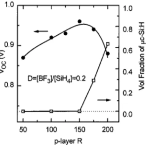
Thus, it is important to re-address this problem by con-sidering state-of-the art solar cells fabricated by multicham-ber PECVD and incorporating p layers deposited using a variation in R according to approach 共3兲 above. In this way, the phase of the p layer can be varied from pure amorphous Si:H through mixed-phase amorphous⫹microcrystalline Si:H 关(a⫹c)-Si:H兴. Figure 1 shows Voc for the series of
n – i – p solar cells incorporating p layers prepared with D
⫽关BF3兴/关SiH4兴⫽0.20, but with different R values over the
range 50⭐R⭐200.
Also plotted versus R in Fig. 1 is the microcrystalline silicon volume fraction in the p layer as obtained by ex-situ SE in the actual n – i – p solar cell configuration. Least-squares regression analyses applying the Bruggeman effec-tive medium theory were performed for the determination of the microcrystalline fractions of the p layers, assuming a three-component mixture of a-Si:H/c-Si:H/void.5 The component dielectric function for single-phase c-Si:H in
these analyses was obtained in studies of a 200-Å-thick p layer prepared on H2plasma treated a-Si:H at 200 °C using a
关H2兴/关SiH4兴/关BF3兴⫽200/1/0.1 gas mixture. This p layer
was measured by RTSE during growth8and then upon cool-ing to 25 °C. The component dielectric function for scool-ingle- single-phase a-Si:H was obtained from an R⫽10 a-Si:H film using ex-situ SE. In Fig. 2, the true optical properties共corrected for surface roughness overlayers兲 are presented for 共a兲 the R
⫽150 p layer with no detectable microcrystalline phase 共⬍0.02 in vol. fraction兲 and 共b兲 the R⫽200 p layer with the
highest microcrystalline content共0.63 in vol. fraction兲, incor-porated within the cells with the highest Voc 共0.96 V兲 and reduced Voc共0.88 V兲 values, respectively. The fact that the p
layer in Fig. 2共b兲 is mixed-phase (a⫹c兲-Si:H, rather than single-phasec-Si:H, may be accounted for by the absence of an i-layer H2-plasma pretreatment.8
The electrical properties of the p layers reveal overall similar trends. For thin 共⬍1000 Å兲 R⫽100 p layers depos-ited on i layers, a thickness-dependent conductivity 共兲 and conductivity activation energy (E) are observed with rela-tively high values of E⬃0.5 eV, attributed to transport dominated by the amorphous phase 共but with an increasing influence of the microcrystalline phase with thickness兲. In contrast, thin p layers with R⫽200 exhibit thickness-independent properties with E⬃0.1 eV, attributed to trans-port dominated by the microcrystalline phase.
Thus, from the overall results presented here, it is clear that the maximum Vocis obtained for the cell incorporating
the p layer deposited at the maximum possible R, while re-maining just below the amorphous-to-共mixed-phase amorphous⫹microcrystalline兲 关a→(a⫹c)兴 transition throughout the 200 Å thickness of the p layer. In fact, this is the same optimization criterion as is applied for one-step i layers to maximize not only Vocbut also the fill factor
sta-bility against light-induced degradation.6Thus, we conclude that Voc is maximized when the p layer is prepared in the
protocrystalline Si:H state and that the overall highest solar cell performance in annealed and degraded states is attained by using protocrystalline Si:H for both p and i layers.
There are two key characteristics that identify the growth regime yielding protocrystalline Si:H.6The first characteris-FIG. 1. Open circuit voltage Voc 共left scale兲 plotted vs the p-layer R
⫽关H2兴/关SiH4兴 value for a series of a-Si:H n – i – p solar cells with one-step R⫽10 i layers 共solid points兲. The p-layer microcrystalline Si:H volume fractions共right scale兲 are also included, as measured by SE in the actual n – i – p cell configuration共open points兲.
1259 Appl. Phys. Lett., Vol. 81, No. 7, 12 August 2002 Kovalet al.
tic is the accumulated thickness dependence of the phase of the growing material. Although the term ‘‘protocrystalline’’ describes an amorphous Si:H phase, given sufficient thick-ness protocrystalline Si:H ultimately evolves—as its name implies—first to mixed-phase (a⫹c)-Si:H and finally to single-phasec-Si:H. A second characteristic of protocrys-talline Si:H is the substrate dependence of the phase evolu-tion. Under protocrystalline growth conditions, microcrystal-line nucleation is suppressed on an underlying a-Si:H film; however, under the same deposition conditions local epitaxy is favored on underlying c-Si:H.
To demonstrate the latter effect, Fig. 2共c兲 provides the dielectric function for the p layer of a n – i – p solar cell fab-ricated under conditions identical to those of the optimum cell of Fig. 2共a兲, with the only difference being the incorpo-ration of a 200 Å R⫽40 interface i layer6 between the R
⫽10 bulk i layer and the overlying R⫽150 p layer. Also
shown in Fig. 3 is a comparison between the resulting solar cell I – V characteristics in the annealed state for共i兲 the op-timum cell of Fig. 2共a兲 with the one-step R⫽10 i layer and the R⫽150 p layer, and 共ii兲 the cell of Fig. 2共c兲 with the two-step R⫽10/R⫽40 i layer and the identically-prepared R⫽150 p layer. Two important effects are observed in Figs. 2共c兲 and 3. First, microcrystalline nuclei at the top surface of the R⫽40 interface i layer, as detected by AFM in p – i – n studies, induce microcrystallites in the p layer. In fact, the volume fraction of microcrystalline phase in the p layer
in-creases from undetectable levels 共⬍0.02兲 to 0.31 with the addition of the R⫽40 interface i layer. Second, Voc of the resulting solar cell drops from 0.96 to 0.77 V due to this increase in p layer microcrystalline fraction. These results further demonstrate that protocrystalline Si:H p layers opti-mize Voc, and that even relatively low substrate-induced
mi-crocrystalline fractions in the p layer are detrimental. In conclusion, we have re-addressed the issue of p-layer optimization for a-Si:H solar cells, finding that the maximum open circuit voltage (Voc) in n – i – p solar cells is obtained
using p layers that are protocrystalline in nature, i.e., depos-ited at the maximum possible R⫽关H2兴/关SiH4兴 without
tra-versing the transition from the a-Si:H growth regime to the mixed-phase (a⫹c)-Si:H regime for the ⬃200 Å p-layer thickness. The higher Voc values may be due to the wider
mobility gaps for the protocrystalline Si:H p layers that are also observed in the case of the i layers.7Owing to the pro-tocrystalline nature of p-layer growth, any microcrystalline silicon nuclei in the underlying i layer, for example, due to excessive H2-dilution, induce microcrystallinity in the p
layer, which reduces Voc.
The authors acknowledge support of this research by NREL 共subcontract Nos. XAF-8-17619-22 and AAD-9-18-668-09兲 and by NSF 共Grant No. DMR-0137240兲.
1S. Guha, J. Yang, P. Nath, and M. Hack, Appl. Phys. Lett. 49, 218共1986兲. 2A. Banerjee, Sol. Energy Mater. Sol. Cells 36, 295共1995兲.
3
X. Deng, S. J. Jones, T. Liu, M. Izu, S. R. Ovshinsky, and K. Hoffman, Mater. Res. Soc. Symp. Proc. 467, 795共1997兲.
4S. Veprˇek, F.-A. Sarott, and M. Ru¨ckschloß, J. Non-Cryst. Solids
137&138, 733共1991兲.
5
R. W. Collins, A. H. Clark, S. Guha, and C.-Y. Huang, J. Appl. Phys. 57,
4566共1985兲.
6J. Koh, Y. Lee, H. Fujiwara, C. R. Wronski, and R. W. Collins, Appl. Phys.
Lett. 73, 1526共1998兲.
7J. Koh, A. S. Ferlauto, P. I. Rovira, C. R. Wronski, and R. W. Collins,
Appl. Phys. Lett. 75, 2286共1999兲.
8J. Koh, H. Fujiwara, R. J. Koval, C. R. Wronski, and R. W. Collins, J.
Appl. Phys. 85, 4141共1999兲.
9J. M. Pearce, R. J. Koval, A. S. Ferlauto, R. W. Collins, C. R. Wronski, J.
Yang, and S. Guha, Appl. Phys. Lett. 77, 3093共2000兲.
10
P. I. Rovira, A. S. Ferlauto, R. J. Koval, C. R. Wronski, R. W. Collins, and G. Ganguly, Mater. Res. Soc. Symp. Proc. 609, A19.6共2000兲.
11R. W. Collins, J. Koh, H. Fujiwara, P. I. Rovira, A. S. Ferlauto, J. A.
Zapien, C. R. Wronski, and R. Messier, Appl. Surf. Sci. 154, 217
共2000兲.
FIG. 2. Real and imaginary parts of the dielectric functions (1,2) of the p layers of a-Si:H n – i – p solar cells incorporating 共a兲 a one-step R⫽10 a-Si:H i layer and R⫽150 protocrystalline Si:H p layer; 共b兲 a one-step R
⫽10 a-Si:H i layer and R⫽200 (a⫹c)-Si:H p layer; and共c兲 a two-step R⫽10/R⫽40 i layer and R⫽150 p layer with substrate-induced (a
⫹c)-Si:H structure.
FIG. 3. Annealed state I – V characteristics for the optimum a-Si:H n – i – p solar cell of Fig. 2共a兲 with the R⫽150 protocrystalline Si:H p layer 共solid symbols兲, and for the n – i – p cell of Fig. 2共c兲 fabricated under otherwise identical conditions, but incorporating a 200 Å R⫽40 Si:H i layer at the i/p junction共open symbols兲.
1260 Appl. Phys. Lett., Vol. 81, No. 7, 12 August 2002 Kovalet al.