HAL Id: hal-03037303
https://hal.archives-ouvertes.fr/hal-03037303
Submitted on 17 Dec 2020
HAL is a multi-disciplinary open access
archive for the deposit and dissemination of
sci-entific research documents, whether they are
pub-lished or not. The documents may come from
teaching and research institutions in France or
abroad, or from public or private research centers.
L’archive ouverte pluridisciplinaire HAL, est
destinée au dépôt et à la diffusion de documents
scientifiques de niveau recherche, publiés ou non,
émanant des établissements d’enseignement et de
recherche français ou étrangers, des laboratoires
publics ou privés.
Control of the deprotonation of terephthalic acid
assemblies on Ag(111) studied by DFT calculations and
low temperature scanning tunneling microscopy
Jeanne Heintz, Corentin Durand, Hao Tang, Roland Coratger
To cite this version:
Jeanne Heintz, Corentin Durand, Hao Tang, Roland Coratger. Control of the deprotonation of
tereph-thalic acid assemblies on Ag(111) studied by DFT calculations and low temperature scanning
tun-neling microscopy. Physical Chemistry Chemical Physics, Royal Society of Chemistry, 2020, 22 (6),
pp.3173-3183. �10.1039/c9cp05151a�. �hal-03037303�
Control of the deprotonation of
Terephthalic
Acid
assemblies
on
Ag(111) studied by DFT calculations
and low temperature scanning
tun-neling microscopy
Jeanne Heintz, Corentin Durand, Hao Tang,
and Roland Coratger
SINANO Group, CEMES/CNRS, 29 rue J. Marvig, 31055 Toulouse, France and Université Paul Sabatier, 118 route de Narbonne, 31000 Toulouse.
E-mail: coratger@cemes.fr
Published in:
Phys. Chem. Chem. Phys. 22(6) (2020) 3173-3183.
https://doi.org/10.1039/C9CP05151A Supplementary Information also available.
1
Abstract
This paper deals with the investigations of Terephthalic Acid (TPA) molecules deposited on a low reactive Ag(111) surface and studied by scanning tunneling microscopy (STM) at low temperature and DFT calculations. These investigations show that two deprotona-tion states energetically equivalent can be produced at the single molecule level. On self assemblies, the mobility of H atoms at 77 K favours the motion of created defects in the layer. The STM obser-vations and DFT calculations show that the most stable structures are obtained when only one hydrogen atom is removed from a O-H...O bond and when these deprotonated molecules are located in adjacent TPA rows.
2
Introduction
The study of self-assembled molecular layers on metal surfaces is of fundamental importance for the development of functional mate-rials and molecular devices1. Among the possible candidates,
ben-zoic acids are known to be model systems to characterize the role of molecular interactions in the synthon structure2. Indeed, these
molecules are able to produce self assemblies mainly bonded by weak hydrogen interactions and whose geometry can be easily pre-dicted by using the appropriate tectons. Thus, linear molecules will tend to produce 1D chains after adsorption while threefold moi-eties will give open-honeycomb networks able to behave as host structures3. The carboxyl groups can also produce carboxylate and metal-ligand bonds leading to specific networks4–7. Among the above mentionned molecules, terephthalic acid (TPA) is one of the most frequently used molecular linkers for the fabrication of 3D metal organic frameworks (MOFs)8,9. When assembled in
2D by hydrogen bonds, its adsorption properties have been studied on different metallic surfaces such as Cu(110)10, Pd(111)11and Au(111)12as well as on Si(111) and passivated Si(111)-√3 ×√
3-Ag substrates13. These molecules are also able to form 2D
metal-ligand coordination arrays for example with magnetic atoms such as the high-spin Fe(TPA)4 assemblies obtained by Gambardella et
al. on Cu(100) surfaces and conducive to investigations concern-ing magnetic anisotropy14. On the same surface, different stud-ies demonstrate the formation of three different lattices depend-ing on the temperature of the metallic surface durdepend-ing molecule deposition, these networks being also linked to a partial or total deprotonation of TPA2,15,16. Recently, White et al. use the same molecules on Cu(111) as a model system to study the well-known interplay between intermolecular and adsorbate-substrate inter-actions17. The possible deprotonation states of these molecules, the intermolecular interactions inside the layers as well as the role of the H atoms appear of fundamental importance for the under-standing of the self assemblies. On a reactive surface such as Cu, the molecule-surface interactions are very important. In this case, deprotonation already appears during the first stages of the self-assembly and once the first hydrogen bonds are formed as sug-gested in Refs18and19. Thus, the choice of a less reactive substrate appears as the possible way to study and control these deprotona-tion states.
In this paper, the low reactive Ag(111) surface has been used to study the controlled deprotonation of TPA single molecules as well as its impact on self-assemblies. The deprotonation state of the molecules can be produced either by a soft thermal annealing or directly using the scanning tunneling microscopy (STM) tip. Two different states of deprotonation can be created in good agreement with the equivalent energy paths calculated by DFT. STM images and DFT calculations demonstrate that H atoms coming from bro-ken OH bonds diffuse on the surface and favour the displacement of the created defects between adjacent rows. These investigations have been also conducted at the single molecule level and show that a local deprotonation can be carried out by the STM tip using the electric field in the tunneling junction. In this case, the cal-culated energy path shows that the two deprotonation states are equivalent in good agreement with the experimental results.
3
Experimental details
STM experiments have been performed at liquid nitrogen temper-ature (T = 77.8 K) for self assembly observations and at liquid helium temperature (T=4.5 K) for single molecule experiments on a commercial STM (LT Omicron) working with a base pressure of 2.10−11mbar. The Ag(111) crystal was cleaned by repeated Ar+
bombardment cycles at E = 500 eV followed by annealing at 780 K for 45 minutes. Once the Ag(111) surface was clean, the molecules were evaporated from a quartz crucible heated by a W wire 0.25 mm in diameter. This evaporator was first pumped by a turbo molecular pump during at least 12h before deposition. Evapora-tions on the substrate held at room temperature were performed in the preparation chamber. The deposition rate was about half a monolayer per minute. Afterwards, the substrate was transferred to the STM chamber to be cooled down at the desired tempera-ture. Evaporations have also been conducted on a cold substrate. For this, the sample was removed from the STM head and placed 5 centimetres above the crucible to reach the same evaporation rate. The deposition was performed during less than one minute and the sample was immediately reintroduced on the STM head to
be cooled down. The whole process took about 1 minute and it is estimated that the sample temperature never exceeded 120 K. In a third type of experiment, the evaporations were performed directly on the STM head through a small hole 1 mm in diameter drilled in one of the cryostat windows. The small solid angle between the source and the substrate supports very small evaporation rates with a typical value of 1/1000 monolayer per second. In this case, the inner cryostat was filled with liquid helium. These conditions were used for single molecule experiments in which thermal diffu-sion has to be inhibited and ultra low coverages are essential. STM tips made of tungsten wires 0.2 mm in diameter were prepared by electrochemical etching and cleaned in UHV using direct current heating. In the text, the indicated bias voltage was always applied to the sample.
4
Theoretical methods
The density functional theory (DFT) calculations were carried out by using the 5.4.4 version of VASP (Vienna Ab-initio Simulation Package)20,21. For these calculations, the valence electronion core interaction was described by the projector augmented wave (PAW) method in a plane wave basis set22. The exchange-correlation interaction was considered within the Perdew-Beck-Eneker (PBE) method in the generalized gradient approximation (GGA)23. The
van der Waals (vdW) interaction was considered with a modified version of DFT-D2, an semi-empirical correction method proposed by Grimme24. The cut-off of the kinetic energy was set to 440 eV, which optimized the silver fcc crystal with a lattice parameter of 4.162 Å. The self-consistent electronic convergence criterion was set to 10−6 eV and the geometrical relaxation was considered to be converged when the forces on each unfixed atom were lower than 0.02 eV/Å. For the adsorbed single TPA molecule, the surface of Ag(111) was described by a 4 atomic layers slab composed of 192 Ag atoms with lateral dimensions 23.53 x 1.543 nm2. For the
self-assembled monolayer, the Ag(111) surface was described by a 4 atomic layers slab of 11.77 x 20.61 Å2 with 128 Ag atoms and
four TPA molecules along the [110] direction (2x2 TPA unit cell). The Brillouin zone was sampled with only the gamma point in the reciprocical space for preliminar calculations and a 3x3 in-plane Monkhorst-Pack grid25for the final results. The vacuum space was set to about 17 Å (above the molecules, and about 20 Å from the Ag surface) in order to minimize the interaction between neighbor supercell in the z direction. The dipole correction was also consid-ered in the z direction to avoid the artificial interaction between periodic cells due to the interface dipole.
The activation barriers for dehydrogenation and diffusion of the TPA molecule and diffusion of the ponctual defects in the TPA monolayer were calculated by applying the two-step procedure proposed by J. Björk26. In that procedure, the transition states were obtained. The Climbing Image Nudged Elastic Band (CI-NEB) method as implemented by the Henkelman group (at UT Austin) was used at first27,28. With this method, the minimum energy re-action path was identified, by optimizing the forces perpendicular to this path to be lower than 0.5 eV/Å on each of equally sepa-rated intermediate conformations. As a second step, the rougly optimized transition state configuration and the images just before and after it were used as the input for the Dimer method29,30. The
final transition state was obtained when the forces on each atom of the central conformation were converged at 0.02 eV/Å.
5
Experimental results
5.1 Deposition at room temperature
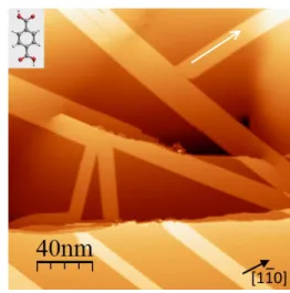
Fig. 1 STM image of a Ag(111) surface after deposition at room temper-ature of TPA molecules (Vbias=0.6 V, I=2 pA, T=77 K). The angle between
the white arrow and the [110] direction is 7◦. The inset shows the molecule
structure.
In these first experiments, the molecules were evaporated in the preparation chamber on the Ag substrate held at room tempera-ture. A large scale STM image of the surface after molecule depo-sition is presented in Fig. 1. It shows the characteristic brickwork structure already reported in previous investigations on low re-acting surfaces12,13,31. The submonolayer coverage results in the formation of molecular bands extended over several hundreds of nanometers. These bands cover the flat terraces but also the de-fects such as steps or screw dislocations present on the surface. During this carpet-like growth, the molecular chains are organised according to the same structure.
Fig. 2 STM image of the TPA network (Vbias=0.6 V, I=50 pA, T=77 K).
The white arrow gives the direction of the molecular band as in Fig. 1.
pre-sented in Fig. 2. The molecules form an oblique network with a lattice parameter of 0.75±0.05 nm and an angle of γ=102±3◦ similar to the structure already reported by Suzuki et al.13. They
are coupled head to tail through linear [O-H...O] bonds between carboxylic end groups giving rise to a marked 1D character along the length of the molecule (see the white arrows in Fig. 1 and Fig.2). Each molecular chain is separated by 0.6±0.05 nm from its neighbours. The apparent height of these domains relative to the Ag(111) surface is about 0.13 nm for a bias voltage of 0.6 V. This value remains almost constant within the bias voltage range used in these experiments. No direct relation between the band ori-entations and the dense <110> or <211>-type directions of the substrate has been found and the measured angles are arbitrary (an example is given in Fig. 1).
Fig. 3 dI/dV spectroscopy performed on the Ag(111) substrate (blue curve) and the TPA self-assembly (red curve) (Vbias=0.2 V, I=30 pA, T=77
K, ∆V=20 mV, f=425 Hz).
The electronic structure of these molecular layers has been also investigated. For this, dI/dV spectroscopic measurements have been conducted on the Ag(111) surface and on the TPA layer and are presented in Fig. 3. The blue curve presents the characteris-tic onset of the Ag(111) surface state at about 60 meV below the Fermi level. This feature is attributed to the well-known surface state band present on the (111) surfaces of noble metals32–34. When the spectra are performed on the molecular layer, an up-ward shift is observed and the feature now appears at about 50 meV above the Fermi level (red curve). Such a phenomenon has already been observed for NaCl(100) ultra thin layers deposited on Cu(111) surfaces35. In this case, the surface band forms an in-terface state confined between the two materials and presenting a modified dispersion relation with respect to the bare metallic sur-face. For the TPA domains, the energy shift is 110±10 meV, a value lower than the one observed for NaCl on Cu (230 meV). A higher value is expected for NaCl because of the high ionic character of this compound with respect to a TPA layer35.
5.2 Evolution of the self-assembly
During these investigations at low temperature, the lattice struc-ture did not change in time. However, the appearance of the molecules inside the assembly evolves when the sample is gen-tly annealed at a sufficient temperature, typically 30 minutes at about 370 K. Above this temperature, molecular desorption takes place and the self-assemblies disappear step by step from the sur-face. The same result can also be reached if the sample is simply
held at ambient temperature during several days. After this kind of experiment, some molecules in the domains present unexpected dark contrasts as illustrated in Fig.4.
Fig. 4 STM image of a TPA domain on Ag(111): the sample was left at room temperature during five days (Vbias=-1 V, I=30 pA, T=77 K).
On this image, a molecular domain close to a step (lower left part of the topography) is presented. Then, dark features ran-domly distributed on the assembly can be detected (the three dark holes on the substrate appearing in the upper part of the image are due to well-known sulphur defects always present near the sil-ver surface36. These features on the molecular domains have not
been observed before and appeared only after annealing. Their apparent depth is about 50 pm for a bias voltage of 100 mV. These dark contrasts look like those presented by White et al17for TPA
on Cu(111) but without the structural difference reported by these authors. Indeed, during our experiments, the intermolecular dis-tances around the defects remain identical to those measured in the pristine lattice. Previous investigations on these molecules demonstrate that these defects are related to the partial depro-tonation of the TPA2,16,18. Indeed, these latter are not due to the presence of a vacancy in the assembly but to a subtle modification of the contrast between two TPA. As a consequence, these defects are assumed to be due to the partial or total deprotonation of the molecule induced by the thermal treatment.
Fig. 5 STM images of TPA assemblies after successive annealing: a) t=135mn, T=370 K. b) t=195mn, T=370 K. c) t=315mn, T=370 K (tunneling conditions: Vbias=0.6 V, I=15 pA, T=77 K).
Thereafter, several annealing at 370 K have been performed of the same sample, starting from a pristine TPA network (Figs. 1 and
2). The evolution of the self assemblies are presented in Fig. 5. Af-ter a first annealing of 45 minutes at 370 K, the density of defects is similar to the one observed in Fig.4. This means that such a ther-mal treatment is equivalent to a stay at ambient temperature for several days. After a second anneal at the same temperature but for an additional 90 minutes, the number of defects substantially increases (Fig. 5a). In the same way, large scale images show that the domain size raise up since molecular diffusion is thermally ac-tivated. Due to the low molecule/substrate interaction, the largest domains grow while the smallest disappear. This tendency is also observed during the next two experiments (Fig. 5b and c) in which the defect number increases in relation with the total annealing time. The radial distribution function (RDF) of Fig. 5c has been calculated and is presented in Supplementary Materials. Indeed, a remaining charge on each defect due to its deprotonation state could induce a minimum distance with the other charged sites lo-cated in the neighborood due to electrostatic repulsion. However, the calculated RDF does not present such a phenomenon indicat-ing that the position of the defects cannot be related to an interac-tion between charged molecules. On the contrary, the distribuinterac-tion shows that the measured lateral distances cover all the possible sites around the deprotonated molecules with a rather monotonic decreasing probability for large distances as expected and without any peaked correlation. This suggests that such an electrostatic in-teraction does not take place mainly because of the predominant presence of the metallic substrate and its screening properties for such small local charges. To establish a clear relation between the number of deprotonated molecules and the total annealing time, the percentage of defect number with respect to the total num-ber of molecules has been calculated using data processing and is reported in Fig. 6.
Fig. 6 Evolution of the number of deprotonated molecules in terms of total annealing time at 370 K deduced from data processing of the STM images.
The graph shows that the defect number increases linearly in terms of total annealing time. At 370 K, the maximum anneal-ing time is slightly below 350 minutes. Below this duration, the domain size increases but the number of observed domains sub-stantially decreases and their presence is more and more rare. Be-yond this value, almost all the molecules desorb from the metallic surface. Thus, the deprotonation is closely linked to the thermal treatment applied to the molecules before their complete
desorp-tion.
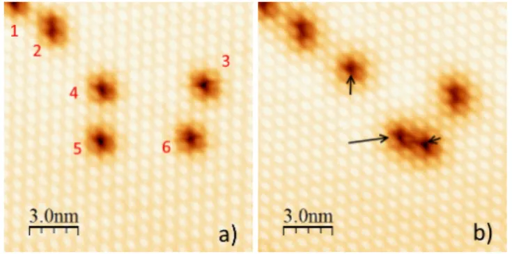
On the different images, it also appears that some of these de-protonated molecules are unstable, i.e. they induce instabilities of the tip. A sufficient positive bias voltage (typically 1.2 V) associ-ated with a relative high current (about 50 pA) induces the spon-taneous displacement of some defects during the tip scan. This can be observed while scanning the same area and recording suc-cessive images. The two images presented in Fig.7 show the same area scanned at 100 mV. Between the two images, this area has been scanned at 1.2 V with the same tunneling current and same scan frequency. The different defects shown in Fig.7a are labelled from 1 to 6. Only 1 and 2 stay in the same position. On the other hand, objects 4, 5 and 6 move between the two images. Moreover, object 3 is slightly modified: an extension appears on its bottom part. Thus, a second defect has been created during the interme-diate scan at "high" voltage.
Fig. 7 a) STM images of six defects. b) Image of the same area after an intermediate scan at 1.2 V showing the displacement of some defects (∆t=30 s). The black arrows show the displacement of the objects 4, 5 and 6 (Vbias=100 mV, I=50 pA, T=77 K).
The dark arrows show the travel done by the mobile defects as well as their length. Thus, during a time interval of 30 seconds, the jump lengths can reach three intermolecular distances (this latter corresponds to the lattice parameter in the self-assembly), i.e. about 2 nm and along precise directions with respect to the TPA rows (−→a or −→b directions in Fig. 2). With these tunneling conditions, this is the maximum distance travelled by these defects. Generally, most of the jump lengths are of one lattice parameter distance (0.75 nm typically). The presence as well as the mobility of these defects suggest that they consist of single hydrogen atoms diffusing on the surface and exchanging their place between fully protonated and deprotonated TPA (such a substitution implying simultaneously the two H atoms between two molecules in a chain, is statistically impossible). This point will be discussed in the DFT calculations (Section 5).
These defects are not only present within the domains after soft annealing but can also be produced by the tip. Indeed, a local in-crease of the bias voltage above 1.2 V generally leads to the forma-tion of defects. Likewise, the extension of the defect 3 in Fig. 7 is assumed to be due to the same tip effect. A more precise example is presented in Fig. 8, the voltage pulse location being indicated by white arrows. Starting from a pristine TPA domain, a first pulse of 1.2 V during 100 ms has been performed in the center of the domain and produces a defect exactly below the tip location. The
Fig. 8 STM image of a molecular assembly after two bias pulses at 1.2 V (during ∆t=100 ms). The white arrows indicate the pulse location: the first has been performed in the center of the band and the second close to the edge (Vbias=400 mV, I=5 pA, T=77 K).
second pulse has been conducted with the same conditions close to the right edge of the assembly but its consequences are different. Two defects have been produced, one exactly below the tip and the second in the adjacent TPA row. Each voltage pulse generally pro-duces this kind of structures but the precise location of the defect cannot be assured. It is also possible to create large areas of defects by increasing the voltage above 1.5 V. This phenomenon appears irreversible since once a defect is created, it can be slightly moved has previously discussed but the defect cannot be cured. As for the thermal annealing, this kind of result is in good agreement with the controlled deprotonation of the molecules. At a sufficient bias voltage, the electric field in the tunneling junction combined with the catalytic role of the metal is able to produce the removal of a single H atom from a TPA. This can also explain the uncertainty in the location of the defect below the tip because the efficiency of the mechanism depends on the field distribution, itself related to the tip apex shape. All these experiments demonstrate that sin-gle H atoms can be removed from TPA domains either using a soft thermal annealing or with the electric field produce at the tip apex.
5.3 Experiments at the single molecule level
In order to complete these observations, experiments on single molecules have been also conducted at liquid helium temperature. For this, evaporation has been performed directly on the metallic surface held at 4.5 K and using ultra low deposition rates. This results in the deposition of isolated molecules as presented in Fig. 9.
Each molecule appears as a slightly elongated protrusion which apparent corrugation is 80±4 pm (with these tunneling condi-tions). These protrusions present a diameter of about 1.35±0.08 nm in good agreement with the distance of 0.95 nm between the most distant H atoms of TPA. Since TPA is physisorbed on the Ag surface, the tunneling current has to be rather low (typically a few
Fig. 9 STM image of three TPA molecules after evaporation on the Ag substrate held at liquid helium temperature. The inset shows the apparent corrugation of a molecule with respect to the metallic substrate (Vbias=800
mV, I=2 pA, T=4.5 K).
picoamps) to avoid molecule displacement. Physisorption of sin-gle TPA also results in the absence of spectroscopic features that could be due to the molecule electronic levels (contrary to the self-assemblies where the metallic surface state is shifted above the Fermi level and becomes an interface state). The electronic surface state around the molecules is not disturbed, contrary to what is ob-served on Cu(111) where dark depressions appear on the molecule extremities simply after their adsorption on the susbtrate17.
On these single molecules, the same voltage pulses that those previously described have been applied. Most of the time, these pulses do not produce any effect except some minor displacements of molecules. To observe real modifications of these molecules, it is necessary to increase the bias voltage, typically above 1.5 V (with ∆t=100 ms). This threshold value is more important than for molecules organized in the self assemblies. The main difficulty for these modifications is the displacement of the molecules below the tip when a pulse is applied. In addition, the tip apex plays an important role in the field distribution in the STM junction. When TPA is embedded in the 2D layer, the location of the defects produced by the tip cannot be precisely planned. Thus, when the experiments are performed on single molecules, a larger electric field has to be produced to modificate them successfully and this can explain the larger voltage that has to be used in this case.
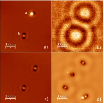
These voltage pulses performed on single molecules induce dif-ferent defects reported in Fig.10. Fig.10a presents the two types of defects stable in time produced by this process. The first one, called "a" type, consists of a small depression on one of the elon-gated parts of the molecule. Its apparent depth is about 30 pm with respect to the Ag surface while the central protrusion exhibits almost the same height than previously observed in Fig. 9 (about 70 pm). A close inspection of this defect shows that the depres-sion is located at 30◦ of the principal axe of the protrusion. One
Fig. 10 STM image of single TPA molecules after evaporation on the Ag substrate held at liquid helium temperature. a) Two type of defects "a" and "b" produced by a voltage pulse on each molecule (for imaging Vbias=500
mV). b) dI/dV image of the same area showing the quantum oscillations of the electron gas and the larger contrast on the double deprotonated TPA ("b" defect) (for imaging Vbias=95 mV). c) Creation of a "b" defect from a
"a" defect produced by a new voltage pulse (for imaging Vbias=500 mV). d)
Creation of a third type of defect called "c" after a new pulse on the second molecule (Vbias=60 mV). Pulse parameters : pulse duration ∆t=100 ms,
Vpulse=1.6 V. Imaging parameters: I=10 pA, T=4.5 K. Locking parameters:
∆V=20 mV, f=425 Hz.
around the molecule, their center being slightly displaced towards the produced depression. These perturbations are due to inter-action of the molecule with the metallic substrate and are not ob-served before the bias pulse (see Fig. 9). The second type of defect, called "b", presents two depressions around the central part of the molecule, giving a symmetrical shape to this structure. For this ob-ject, the apparent height of the center significantly decreases from 70 pm to 12 pm. On the other hand, the depressions are slightly deeper than for the a type (40 pm instead of 30 pm). A spectro-scopic dI/dV image of the area has been performed simultaneously and is presented in Fig. 10b. For this, a small modulated voltage of 20 mV at 425 Hz has been added to the constant bias of the tun-neling junction. This image shows that these two defects produce an important diffusion of the 2D electronic gas and that this effect is more important for the b-type one. Indeed, the amplitude of the dI/dV signal is 0.17 pA for the first type while it reaches 0.21 pA for the second.
These two types of defects are stable in time. They can also be moved on the surface using the STM tip but with more difficulty than for TPA: for example the imaging current can be significantly increased above 10 pA without any important motion of the de-fects. Fig.10c highlights another characteristic. The STM image shows the same area but after a second bias pulse of 2.2 V has been applied to the top molecule (previously an "a" type). In this case, this molecule switches and then exhibits a "b" shape. It means that
a and b types are closely linked and correspond to similar mecha-nisms inside a single molecule.
A third type of defect formed by successive bias pulses is also observed (called "c" in Fig. 10d). It consists of an asymmetrical structure in which one of the dark lobes of the b shape decreases in size while the corrugation of the central part disappears. In addition to its particular shape, this object is highly unstable and mobile on the surface. While the "a" and "b" forms are rather sta-bilized by the voltage pulse suggesting a larger interaction of TPA with the substrate after the modification, this third type of defect generally disappears after a few scans. It is assumed that in this case, the TPA molecule is fragmented. Then, the interaction with the substrate vanishes and the adsorbate looses it stability. The "a" and "b" type objects can be produced using another derivative method. For this, the tip is withdrawn of 1 nm from the surface and the bias voltage is increased up to 2.8 V. A high electric field is then produced all around the tip location. In this perimeter (about 10 nm in diameter), all the molecules are switched in "a" or "b" form, independently of their position with respect to the tip apex. However, this last method is less accurate than the one using small bias pulses. Indeed, using a bias voltage of about 1.8 V, it is pos-sible to switch the molecules into the "a" state only, even if the switching yield is not exactly 100%. With the second method, the results of the switch are randomly distributed between the "a" and "b" forms. In every cases, these mechanisms are irreversible. Once a form is produced, it is impossible to come back to the original conformation. Manipulations with the STM tip also show that it is impossible to exchange one of these defects with an intact TPA molecule. For example, in the bottom part of Fig. 10d, a defect (b type) and a protonated TPA have been brought closer using atomic manipulation without it being possible to modify the defect at the expense of the molecule.
Previous investigations on single objects have demonstrated that these observations are due to different deprotonation states of the molecules induced by the voltage pulses37,38. Recently, Schmitt and co-workers reported deprotonation of biphenyl dicarboxylic acid (BDA) on a Cu(111) surface39. BDA have great similarities with TPA because of their two carboxyl moieties at the two ends of the molecules. After deprotonation, BDA exhibits well-known depressions due to the carboxylate bond to the metallic surface. TPA is known to have the same behaviour on a metallic surface af-ter deprotonation and the formation of a carboxylate with metallic atoms has been previously evoked on different surfaces11,16 but
never directly observed. In addition, Fig. 10 shows that it is pos-sible to control the state of the molecule with one or two depro-tonated carboxyl groups. This also means that the molecules are adsorbed fully protonated which is not surprising if one considers the low reactivity of the Ag(111) surface.
6
DFT calculations
6.1 Adsorption and deprotonation of single TPA molecules 6.1.1 Adsorption parameters
DFT calculations have been performed both at the single molecule level and for the TPA self assembly. For a single molecule, calcula-tions show that TPA is physisorbed on the Ag(111) with an
adsorp-tion energy of -1.43 eV and a van der Waals (vdW) contribuadsorp-tion of -1.61 eV.
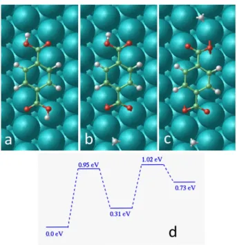
Fig. 11 Top and side views of the adsorption geometries of a single TPA on Ag(111): a) neutral, b) without an H atom and c) without two H atoms.
The C atoms backbone to the surface distance is about 0.29 nm (Fig.11a) which is similar to the 0.29 nm distance measured for ex-ample by X-ray standing waves (XSW) in perylene-tetracarboxylic-dianhydride (PTCDA) on Ag(111)40. This value is then in good agreement with a physisorption of the molecule. Upon adsorption, the Fermi energy is shifted upwards from 0.16 eV, and the cal-culated work function was reduced by 0.07 eV as compared to the bare Ag(111) slab. Then, this physisorption induces a slight charge transfer of 0.14 electron from the substrate to the molecule.
When the TPA molecule has lost one hydrogen atom, the de-protonated carboxylate group becomes strongly attached to the surface with an adsorption energy of -3.51 eV which is accompa-nied with a slight increase of the vdW interaction to -1.68 eV. The carboxylic acid extremity has a distance to the surface similar to the un-dehydrogenated TPA molecule. However, in the dehydro-genated carboxylate group, the O atoms are now situated at 0.21 nm from the Ag(111) surface (Fig.11b). Thus, the bending be-tween the benzene plane and these O atoms is 80 pm, a value more important than the one reported for TPA on Cu(001)16. The total charge transfer is +0.75 electron from the surface to the molecule. Because of this charge transfer, the work function increased by 0.11 eV and the Fermi energy shifted 100 meV upward as com-pared to the bare Ag(111).
When the second hydrogen was cleaved, the two extremities with the carboxylate groups bind by chemical bonding to the Ag(111) surface with an important adsorption energy of -5.51 eV. Consequently, the two ends of the molecule are bent towards the surface (Fig.11c). Due to this strong binding, a total of +1.37 elec-trons are transferred from the surface to the molecule. The Fermi energy is shifted 0.05 eV upwards and the work function increased by 0.26 eV (all these parameters can be found in Supplementary Materials, Table 1). The deformation of the molecule induced by adsorption and deprotonation (80 pm with respect to the central carbon backbone) cannot be observed on the experimental STM images because each molecule appears as a protrusion without any resolution inside the molecular skeleton. At this scale, the STM features are mainly related to the density of electronic states. The DFT results show that the interaction with the substrate in-creases as a function of deprotonation state mainly because of the binding of one or two carboxylate groups with the metallic atoms.
In the same way, the STM images present two different configu-rations (a and b in Fig. 10) as a function of their deprotonation state. Thus, the dark areas located in the molecule extremities can be associated to the carboxylate parts in chemical interaction with the metallic atoms. The so-induced charge transfer (0.75 and 1.37 electrons respectively), the subsequent increase of the work fonc-tion (+0.11 and +0.26 eV respectively) and their effects on the local density of states could perfectly explain this phenomenon. Experimentally, the carboxylate formation on deprotonated single TPA is also revealed through the formation of well-known oscil-lations of the 2D electron gas in the spectroscopic dI/dV images. Thus, the oscillation amplitude measured by STM increases with the deprotonation state (Fig. 10b) revealing the increasing chemi-cal interaction of the molecule ends with the silver atoms.
Fig. 12 Top views showing DFT calculations of a single TPA adsorbed on Ag(111): a) neutral, b) without an H atom and c) without two H atoms. d) shows the activation energies for these conformations.
6.1.2 Deprotonation of a single molecule
From the DFT approach, the barrier to break a first O-H bond from a neutral TPA molecule has been calculated to be 0.95 eV (these calculations are reported in Fig. 12). The singly dehydrogenated TPA with the detached hydrogen atom adsorbed close by, has an energy 0.31 eV higher than the neutral one. Starting from this state, the energy barrier to break the second O-H bond of the molecule is 0.71 eV, still with the detached hydrogen atom ad-sorbed close by. To dehydrogenate directly these two H atoms (without desorption of an H2 molecule), it is necessary to
over-come a barrier of 1.02 eV (Fig. 12d). This result is consistent with the fact that experimentally, a bias voltage slightly higher than 1.5 V could produce both of "a" type and "b" type forms, which are attributed to singly and doubly deprotonated TPA respectively. In the activation barrier calculations, the free diffusion of H atoms is not considered, neither the desorption of H2molecule after
and the H-H recombination barrier were estimated as 3.1 kcal/mol (0.13 eV) and 12.6 kcal/mol (0.55 eV) respectively. The dehydro-genation reactions are endothermic. The reverse reaction pathway corresponds to re-attach the free H atoms with an activation bar-rier of 0.29 eV and 0.64 eV respectively. As the single molecule is only stable at 4.5 K on the metallic substrate, it is not possible to re-attach at low temperature these H atoms spontaneously without activation. This explains that once the molecule is deprotonated using the STM tip, it is impossible to turn back.
6.2 TPA self-assembly
The problem is more difficult when the molecules are embedded in a self-assembly because the H atoms may diffuse on the molec-ular layer and interact with the surrounding molecules. For TPA molecules self-assembled in a monolayer (ML), the physisorption energy for the 2x2 TPA unit cell (considered in the following as the neutral ML) is -7.76 eV, which corresponds to an adsorption energy of -1.94 eV per molecule. This energy is stronger than the physisorption energy of single TPA molecule (-1.43 eV). This differ-ence is due to the intermolecular H-bonds and vdW forces which take place in the TPA domains (see table 2 in Supplementary Ma-terials). Indeed, the molecule-surface contribution per molecule (-1.64 eV) is similar to that of the single molecule (-1.61 eV).
With one singly dehydrogenated TPA inside the ML unit cell (sin-gle defect), the total adsorption energy is -9.94 eV, i.e. 2.18 eV stronger than the adsorption energy of the neutral ML. This dif-ference between the neutral and singly dehydrogenated ML is al-most the same as in the case of single TPA on Ag(111) (2.08 eV). With one doubly dehydrogenated TPA molecule embedded, the ad-sorption energy of the 2x2 cell is -11.70 eV, i.e. 3.94 eV stronger than the neutral ML. This difference is slightly lower than in the case of single TPA on Ag(111) (4.08 eV). That means that, once a molecule is deprotonated (singly or doubly), the difference of adsorption energy is the same for the whole system whether its is a single molecule or a complete layer. In this case, a TPA is chemically bound to the substrate and this does not depend on its surrounding. Thus, the chemical bond plays the major role in the adsorption calculations.
With two singly dehydrogenated molecules (i.e. two single de-fects in the unit cell), the adsorption energy of the 2x2 unit cell is -11.95 eV. In this case, each molecular chain (i.e. each 1D TPA wire stabilized by double H-bonds) has only one singly dehydrogenated molecule. This energy is -11.86 eV when the two dehydrogenated molecules were originated from the same double H-bonds dimer in the same 1D chain (double defect). The difference in adsorption energy with the neutral 2x2 TPA unit cell is slightly above 4 eV for these two configurations which suggests that these two types of de-fects do not significantly alter the stability of the monolayer. How-ever, the conformation in which two molecules are deprotonated in different 1D chains, leads to the most stable conformation (90 meV lower than the double defect). The Fermi level of the neutral TPA ML has increased drastically compared to that of the single molecule (upwards shift of 0.67 eV v.s. 0.16 eV for single TPA). This large Fermi energy difference is consistent with the fact that in a ML, the Ag(111) surface is fully covered by TPA molecules.
Thus, the increase of the Fermi level is enhanced for a complete molecular layer with respect to its position for the bare Ag surface. The presence of singly or doubly dehydrogenated TPA among all the other molecules only induces small shifts of EF. Thus, the most
important effect of the self assembly is the significant upward shift observed in the Fermi level, the two deprotonation states having only a small influence of the calculated energies (all the calculated parameters for the 2x2 TPA unit cell are reported in Table 2 of Supplementary Materials).
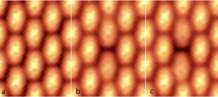
Fig. 13 Calculated STM images of a TPA self-assembly: a) neutral mono-layer, b) with only a deprotonated TPA in the center and c) with a double defect (two H removed in the hydrogen bond between two TPA of the same row).
It is also interesting to study the influence of the deprotona-tion states to the STM topographies performed on the molecular assemblies. For this, STM images of the neutral ML, a ML contain-ing a scontain-ingle defect and then, a double defect have been calculated by using an extended Hückel theory based program in which the tunneling current was evaluated with a formalism based on the Greens function method42,43. In the calculated images presented in Fig. 13, small contrast differences in the three cases (neutral, single defect and double defect) can be distinguished. Plotting the iso-value surface of the local density of states (LDOS) for these three assemblies also confirms these results. Such small differ-ences between the LDOS with and without the defects should only induce small corrugations in the STM images. This is exactly what is experimentally observed since the maximum corrugation on the deprotonated areas (produced by thermal annealing or by the STM tip) is only 40 pm.
6.3 Diffusion of H atoms 6.3.1 Single defects
During the STM experiments, it has been observed that the defects due to deprotonation of TPA can move during the tip scan (Fig. 7). This point has been theoretically investigated starting from an unit cell in which an H atom has been already removed. In this case, the first detached H atom is considered to have diffused far away or desorbed as H2molecule when recombined with another freely
diffusing H atom. The activation barrier to break a second O-H bond has been calculated. Surprisingly, a new H atom migration pathway has been identified and is presented in Fig. 14.
This latter can be described as the exchange of an H atom com-ing from a normal O-H...O bond to the already deprotonated bond of a neighbouring row. This pathway has two transition states
sep-Fig. 14 Activation barrier calculated for H exchange between TPA rows. a) Initial state with one H atom removed from a TPA of the right row (en-circled). b) Intermediate state. c) Final state with the H defect located on the left row (encircled). d) Energy path including the two transition as well as the intermediate states.
arated by an intermediate state with a slightly lower total energy (-0.16 eV). The negative value of the intermediate state suggests that this conformation should be the most stable. However, this small numerical value does not represent an absolute result mainly be-cause of the limited dimensions of the periodic super-cell slab and its consequences on the energy calculations. This simply suggests that there is a minimum between two transition states and this minimum is used to calculated the energy barriers. The first one is 0.5 eV higher than the initial state, and the second barrier between the intermediate state and the second transition state is 0.67 eV. When the activation energies are high enough to overcome these two barriers, it is possible to induce a migration between these two quasi degenerated singly dehydrogenated states. This H atom migration pathway could also be considered as the migration of single deprotonated defects, which are observed during the scan at a bias of 1.2 V at 77 K (Fig. 7). As the activation barriers of this migration are much lower than the barrier necessary to detach a first H atom from the neutral ML (0.95 eV), it is possible to induce H migration at this relative low voltage without generating new defects. However, it is important to note that due to the periodic super-cell, the density of dehydrogenated defects is much higher than in experiments. This migration can also explain the difficulty to create defects immediately below the tip apex. Indeed, once created, the defects can diffuse, thanks to the H migration, and induce the apparition of "new" defects a few tenth of nanometers from the tip apex (Fig. 8).
6.3.2 Double defects
Another question comes from the stability of single and double defects. Remember that in the first type of defect, a single H atom is removed from the TPA raw while in the second, the two H atoms implied in the hydrogen bond between two TPA have disappeared. In order to study this stability, the possibility to migrate one H atom implied in the O-H...O bonds in a TPA row to an neighbouring double defect located in the adjacent row has been investigated.
Fig. 15 Activation barrier calculated for H exchange between TPA rows. a) Initial state with two H atom removed from a TPA row (encircled). b) Intermediate state. c) Final state with the migrating H located on the right row and the presence of two single defects. d) Energy path including the two transition as well as the intermediate states. e) STM image of the TPA self-assembly after thermal annealing showing the orientation of the H defects along [10] or [01] directions of the surface Bravais lattice(T=77K).
The identified pathway contains two activation barriers. The initial state is presented in Fig. 15a and corresponds to a double defect in the right TPA row. A first barrier of 0.32 eV between this state and an intermediate state has been calculated (Fig. 15b). A second barrier of 0.5 eV appears between this intermediate state and the final state in which two single defects in two adjacent rows are observed (Fig. 15c). In this final state, one H atom from the left row migrates to the right row to form a second single defect. Fi-nally, this state is composed of two single defects, one on each TPA row. Note that for the intermediate state at -0.14 eV, the remark previously made for the same type of state in Fig. 14d is still avail-able. Reversely, from the double single defect to the double defect, the two barriers are respectively 0.49 eV and 0.46 eV (Fig. 15d). As these barriers have the same magnitude than the diffusion of a single defect as discussed above, the transformation from a double single defect to a single double defect and vice versa should be pos-sible. Concerning the total energy, the double single defect is 0.13
eV more stable than a double defect (another example of possible pathways starting from a defect free ML and demonstrating the stability of single defects is presented in the Supplementary Mate-rials). This point is particularly interesting when compared to the experimental results (Fig. 15e). In this image, the large majority of dark spots are single defects. The darker structures which are double defects are rather rare (less than 0.5%), a result in good agreement with the energy calculation concerning the stability of single deprotonated TPA. When the density of defects is sufficient, which is the case in the presented STM image, the defects are asso-ciated in dimers, trimers, quadrimers or more. The angle between the direction of these groups of defects and the TPA rows corre-sponds to the one observed in Fig. 15c between the line joining two single defects (final state) and the vertical TPA row (about 48±5◦). It also corresponds to the angle between the [10] or [01]
directions of the self-assembly and the TPA row directions (about 50±5◦).
7
Conclusion
The deprotonation of TPA molecules deposited on low reactive Ag(111) surfaces in UHV has been studied by combining LT-STM images and DFT calculations. For stable, individual TPA molecules, a temperature as low as 4.5 K is necessary to prevent diffusion. The deprotonation of these molecules was achieved by applying a tip bias voltage of 1.5 V at least. Then, two energetically equivalent deprotonation states could be created. The mechanism of deproto-nation is attributed to the high electric field produced around the tip location. The slight difference in activation barriers between the single dehydrogenation and the double one is the reason for which these two states could be obtained during a voltage pulse. For self-assembled TPA MLs observed at 77 K, the majority of de-fects created when the samples were kept at RT or moderately annealed at a maximum temperature of 370K are singly deproto-nated molecules, while double defects are rarely observed. This difference agrees with the lower stability of the double defect and with the lower migration barrier of an H atom of a double O-H...O bond dimer to a double defect. Then, most of these later evolve so that each of them forms two single defects. Application of a voltage pulse as for individual molecules, could induce similar de-fects. Some of such defects are displaced after a scan at "high" voltage (typically above 1.2 V). This mobility is explained by the presence of two low diffusion barriers (0.5 eV) separated by an in-termediate state which involves an intermolecular O-H...O bond. The diffusion facility of these defects is similar to the Grotthuss mechanism of fast proton diffusion in liquid water44, and favours
the formation of 1D linear defects dimers, trimers, quadrimers, etc. This possibility could be exploited for the fabrication of one atom thick magnetic wires by coordinating metallic atoms to these 1D structures.
Conflicts of interest
There are no conflicts to declare.
Acknowledgements
This study has been supported through the EUR grant NanoX n◦
ANR-17-EURE-0009 in the framework of the "Programme des
In-vestissements d’Avenir". DFT calculations were performed using HPC resources from CALMIP (Grant 2019-P0686).
References
1 J. V. Barth, Annual Review of Physical Chemistry, 2007, 58,
375–407.
2 S. Stepanov, N. Lin, F. Vidal, M. Rubens, J. Barth and K. Kern,
Nano. Letters, 2005,5, 901–904.
3 N. Lin, D. Payer, A. Dmitriev, T. Strunskus, C. Wöll, J. V. Barth and K. Kern, Angewandte Chemie, 2005,44, 1488–1491.
4 J. Barth, J. Weckesser, N. Lin, A. Dmitriev and K. Kern, Applied
Physics A, 2003,76, 645–652.
5 A. Dmitriev, H. Spillmann, N. Lin, J. V. Barth and K. Kern,
Ange-wandte Chemie International Edition, 2003,42, 2670–2673.
6 A. Dmitriev, H. Spillmann, M. Lingenfelder, N. Lin, J. V. Barth and K. Kern, Langmuir, 2004,20, 4799–4801.
7 T. Classen, G. Fratesi, G. Costantini, S. Fabris, F. L. Stadler, C. Kim, S. de Gironcoli, S. Baroni and K. Kern, Angewandte
Chemie International Edition, 2005,44, 6142–6145.
8 M. Eddaoudi, J. Kim, N. Rosi, D. Vodak, J. Wachter, M. O’Keeffe and O. M. Yaghi, Science, 2002,295, 469–472.
9 G. Férey, C. Mellot-Draznieks, C. Serre, F. Millange, J. Dutour, S. Surblé and I. Margiolaki, Science, 2005,309, 2040–2042.
10 D. S. Martin, R. J. Cole and S. Haq, Phys. Rev. B, 2002, 66,
155427–155435.
11 M. Cañas-Ventura, F. Klappenberger, S. Clair, S. Pons, K. Kern, H. Brune, T. Strunskus, C. Wöll, R. Fasel and J. Barth, The
Journal of Chemical Physics, 2006,125, 184710.
12 S. Clair, S. Pons, A. Seitsonen, H. Brune, K. Kern and J. Barth,
The Journal of Physical Chemistry B, 2004,108, 14585–14590.
13 T. Suzuki, T. Lutz, D. Payer, N. Lin, S. Tait, G. Costantini and K. Kern, Phys. Chem. Chem. Phys., 2009,11, 6498–6504.
14 P. Gambardella, S. Stepanow, A. Dmitriev, J. Honolka, F. de Groot, M. Lingenfelder, S. Gupta, D. Sarma, P. Bencok, S. C. S. Stanescu, P. S., N. Lin, A. Seitsonen, e. H. Brun, J. V. Barth and K. Kern, Nature Materials, 2008,8, 189–193.
15 S. Stepanow, T. Strunskus, M. Lingenfelder, A. Dmitriev, H. Spillmann, N. Lin, J. V. Barth, C. Wöll and K. Kern, The
Journal of Physical Chemistry B, 2004,108, 19392–19397.
16 J. D. Fuhr, A. Carrera, N. Murillo-Quirós, L. J. Cristina, A. Cos-saro, A. Verdini, L. Floreano, J. E. Gayone and H. Ascolani, The
Journal of Physical Chemistry C, 2013,117, 1287–1296.
17 T. W. White, N. Martsinovich, A. Troisi and G. Costantini, The
Journal of Physical Chemistry C, 2018,122, 17954–17962.
18 B. Quiroga Argañaraz, L. J. Cristina, L. M. Rodriguez, A. Cos-saro, A. Verdini, L. Floreano, J. D. Fuhr, J. E. Gayone and H. As-colani, Phys. Chem. Chem. Phys., 2018,20, 4329–4339.
19 M. Uphoff, G. S. Michelitsch, R. Hellwig, K. Reuter, H. Brune, F. Klappenberger and J. V. Barth, ACS Nano, 2018,12, 11552–
11560.
20 G. Kresse and J. Furthmuller, Computational Materials Science, 1996,6, 15 – 50.
21 G. Kresse and J. Furthmuller, Phys. Rev. B, 1996, 54, 11169–
22 P. E. Blöchl, Phys. Rev. B, 1994,50, 17953–17979.
23 J. P. Perdew, K. Burke and M. Ernzerhof, Phys. Rev. Lett., 1996,
77, 3865–3868.
24 S. Grimme, Journal of Computational Chemistry, 2006, 27,
1787–1799.
25 H. J. Monkhorst and J. D. Pack, Phys. Rev. B, 1976,13, 5188–
5192.
26 J. Björk, Y.-Q. Zhang, F. Klappenberger, J. V. Barth and S. Stafström, The Journal of Physical Chemistry C, 2014,118,
3181–3187.
27 G. Henkelman and H. Jónsson, The Journal of Chemical Physics, 2000,113, 9978–9985.
28 G. Henkelman, B. P. Uberuaga and H. Jónsson, The Journal of
Chemical Physics, 2000,113, 9901–9904.
29 G. Henkelman and H. Jónsson, The Journal of Chemical Physics, 1999,111, 7010–7022.
30 J. Kästner and P. Sherwood, The Journal of Chemical Physics, 2008,128, 014106.
31 A. Carrera, L. J. Cristina, S. Bengió, A. Cossaro, A. Verdini, L. Floreano, J. D. Fuhr, J. E. Gayone and H. Ascolani, The
Jour-nal of Physical Chemistry C, 2013,117, 17058–17065.
32 S. Kevan and R. Gaylord, Phys. Rev. B, 1987,36, 5809–5818.
33 R. Paniago, R. Matzdorf, G. Meister and A. Goldmann, Surface
Science, 1995,336, 113 – 122.
34 G. Hörmandinger, Phys. Rev. B, 1994,49, 13897–13905.
35 J. Repp, G. Meyer and K. Rieder, Phys. Rev. Lett., 2004, 92,
036803.
36 P. Avouris, I.-W. Lyo and P. Molinàs-Mata, Chemical Physics
Let-ters, 1995,240, 423 – 428.
37 L. Lauhon and W. Ho, Surface Science, 2000,451, 219 – 225.
38 Y. Kitaguchi, A. Shiotari, H. Okuyama, S. Hatta and T. Aruga,
The Journal of Chemical Physics, 2011,134, 174703.
39 T. Schmitt, L. Hammer and M. A. Schneider, The Journal of
Physical Chemistry C, 2016,120, 1043–1048.
40 S. Duhm, A. Gerlach, I. Salzmann, B. Bröker, R. Johnson, F. Schreiber and N. Koch, Organic Electronics, 2008, 9, 111
– 118.
41 A. Montoya, A. Schlunke and B. S. Haynes, The Journal of
Phys-ical Chemistry B, 2006,110, 17145–17154.
42 J. Cerdá, M. A. Van Hove, P. Sautet and M. Salmeron, Phys.
Rev. B, 1997,56, 15885–15899.
43 J. Cerdá and F. Soria, Phys. Rev. B, 2000,61, 7965–7971.