HAL Id: cea-01974216
https://hal-cea.archives-ouvertes.fr/cea-01974216
Submitted on 8 Jan 2019
HAL is a multi-disciplinary open access
archive for the deposit and dissemination of
sci-entific research documents, whether they are
pub-lished or not. The documents may come from
teaching and research institutions in France or
abroad, or from public or private research centers.
L’archive ouverte pluridisciplinaire HAL, est
destinée au dépôt et à la diffusion de documents
scientifiques de niveau recherche, publiés ou non,
émanant des établissements d’enseignement et de
recherche français ou étrangers, des laboratoires
publics ou privés.
Performance and Transport Analysis of Vertically
Stacked p-FET SOI Nanowires
Bruna Cardoso Paz, Marcelo Pavanello, Mikael Casse, Sylvain Barraud, Gilles
Reimbold, Maud Vinet, Olivier Faynot
To cite this version:
Bruna Cardoso Paz, Marcelo Pavanello, Mikael Casse, Sylvain Barraud, Gilles Reimbold, et al..
Perfor-mance and Transport Analysis of Vertically Stacked p-FET SOI Nanowires. 2017 Joint International
EUROSOI Workshop and International Conference on Ultimate Integration on Silicon
(EUROSOI-ULIS), Apr 2017, Athènes, Greece. �10.1109/ULIS.2017.7962606�. �cea-01974216�
Performance and Transport Analysis of Vertically
Stacked p-FET SOI Nanowires
Bruna Cardoso Paz and Marcelo Antonio Pavanello
Department of Electrical Engineering Centro Universitário da FEI São Bernardo do Campo, Brazil
Mikaël Cassé, Sylvain Barraud, Gilles Reimbold,
Maud Vinet and Olivier Faynot
Département des Composants Silicium – SCME/LCTE CEA-LETI Minatec
Grenoble, France
Abstract—This work presents the performance and transport
characteristics of vertically stacked p-MOSFET SOI nanowires (NWs) with inner spacers and epitaxial growth of SiGe raised source/drain. Electrical characterization is performed for NWs with [110] and [100] channel orientations, as a function of both fin width (WFIN) and channel length (L). Results show a good
electrostatic control and reduced short channel effects (SCE) down to 15nm gate length. Improved effective mobility is obtained for [110]-oriented NWs due to higher sidewall mobility contribution.
Keywords—performance; transport; electrical characterization; vertically stacked nanowire; SOI MOSFET; channel orientation.
I. INTRODUCTION
Multiple gate transistors have been designed to improve the electrostatic control of the gate over the charges in the channel, allowing stronger immunity against short channel effects [1]. Since higher electrostatic coupling is obtained increasing the number of gates and reducing the distance among them, triple gate (3G) and Gate-All-Around (GAA) MOSFETs have demonstrated to outperform short channel FinFETs, attracting interest of both scientific community and semiconductor industry [2].
Nanoscale multiple gate MOSFETs called nanowires, characterized by thin silicon thickness and narrow fin width, have shown to be a good alternative to FinFET technology for the continuity of the CMOS roadmap due to their great performance and scalability [3], [4].
To fulfill higher drive current requests imposed by the International Technology Roadmap for Semiconductors (ITRS), the performance of multiple gate structures have been improved through the development of new technologies and implementation of different materials and process techniques, such as mechanical stress and rotated substrates. While the use of compressive and tensile stress can enhance holes and electrons mobility, respectively [5], [100]-orientated channel can boost n-type NWs current due to higher electrons mobility along (100) sidewalls [6].
Recently, vertically stacked NWs have been successfully fabricated due to advanced process developments. These devices combine reduced SCE and improved on-state current (ION) due to higher device aspect ratio, as the overall channel
width (Weff) is increased and proportional to the number of
beams [7]–[9].
In this work, we present the performance and transport of vertically stacked p-FET SOI NWs fabricated with inner spacers and SiGe raised source/drain [9]. The analysis is performed as a function of both WFIN and L, for NWs
orientated along [110] and [100] directions. Electrical characterization is performed from I-V and C-V curves to evaluate ION/IOFF behavior, gate-to-channel capacitance (CGC),
effective oxide thickness (EOT), threshold voltage (VTH)
roll-off, subthreshold slope (S), DIBL, series resistance (RS) and
effective mobility (eff).
II. DEVICES CHARACTERISTICS
Vertically stacked NWs with two levels have been fabricated at CEA-LETI, starting from SOI wafers with 145nm buried oxide thickness and using a replacement metal gate (RMG) process. TEM images of the cross section (a) and the longitudinal section (b) of the studied stacked-NWs MOSFETs are presented in Fig. 1. It is observed that the wire at the bottom presents a -shaped gate while the wire at the top is GAA. Both levels have a 10nm thick Si channel and Si0.7Ge0.3:B raised source/drain have been used in order to
induce a compressive strain of up to 1% in both top and bottom channels [9]. The transistors have been fabricated along two different crystallographic orientations, [110] and [100], and present a gate stack composed by HfO2/TiN/W. Further
fabrication details of the stacked-NWs studied in this work can
Fig.1. Vertically stacked SOI NW cross section (a) and longitudinal section (b) TEM images.
-1.5 -1.0 -0.5 0.0 0.5 0 5 10 15 20 -1.5 -1.0 -0.5 0.0 0.5 0 50 100 150 200 250 300 |IDS|.L (A.m) VDS = -40mV VGS (V) 45° 0° L=100nm L=30nm 1E-8 1E-6 1E-4 0.01 1 100 VDS = -0.9V WFIN = 15nm 50 fins 1E-5 1E-4 1E-3 0.01 0.1 1 10 100 1000 (a) (b)
Fig.3. |IDS|.L as a function of VGS at VDS = –40mV (a) and –0.9V (b) for
[110] and [100]-NWs, L = 100 and 30nm. 0 100 200 300 400 500 0.1 1 10 100 1000 10 20 30 40 50 60 70 0 1 2 3 4 5 ION/WFIN = 1100A/m for WFIN = 15nm WFIN from 15 to 30nm I OFF /W ef f (nA/ m) ION/Weff (A/m) (a) ION/WFIN = 2500A/m for WFIN = 15nm ION = IDS @VGS=-0.9V IOFF = IDS @VGS=0V L = 30nm VDS = -0.9V 0° 45° ION /IOFF (x1 0 4 ) WFIN (nm) (b)
Fig.4. ION/IOFF characteristics for [110] and [100]-NWs with L = 30nm, at
VDS = –0.9V.
be found in [9].
In order to extract the EOT resulted from the gate stack deposition after RMG process, capacitance measurements were performed and compared to results obtained from a Poisson-Schrödinger solver considering quantum confinement effects for FDSOI MOSFETs. Fig. 2.a presents CGC as a function of
VGS for [110]- and [100]-NWs, WFIN = 45nm and L = 100nm.
The solid line indicate the modelled result considering EOT of 1.2nm. After fitting the experimental C-V curves, 1.2nm of EOT has been extracted for both transport orientations. Fig. 2.b presents CGC as a function of WFIN for NWs biased at the same
gate voltage overdrive (VGT = VGS – VTH = –1V). The linear
behavior, highlighted by the dashed lines, allows to conclude that EOT is sustained with WFIN scaling and channel
orientation, indicating uniform and well controlled gate stack deposition process.
III. RESULTS AND DISCUSSION
Fig. 3 presents the normalized drain current (IDS.L) as a
function of the gate voltage (VGS) for [110] (0°) and [100]
(45°) NWs in multiple finger structures (50 fins), with L = 30nm and 100nm, at small (a) and strong (b) horizontal electric field, VDS of –40mV and –0.9V, respectively. Higher drain
current is observed in [110]-NWs, as expected for p-FETs. Indeed, holes mobility is enhanced in the (110)-oriented sidewalls in comparison to (100) plan [10]. Additionally, the SiGe source and drain induce a uniaxial compressive stress, which may become detrimental in narrow p-NWs with [100]-oriented channel. As reported in [11], the longitudinal piezoresistive coefficient of [100]-oriented NWs are lower than zero (see Fig. 5 in [11], whereL,NW[100] < 0), which degrades
even more the holes mobility in such narrow devices. From the logarithmic scaled curves in Fig. 3, it is possible to state that neither by reducing L from 100nm to 30nm nor by decreasing VDS down to –0.9V significant degradations of the
subthreshold characteristics are observed.
Fig. 4 presents IOFF/Weff as a function of ION/Weff (a) and
ION/IOFF as a function of WFIN (b) for L = 30nm, at VDS = –
0.9V. IOFF and ION have been extracted at VGS = 0 and –0.9V,
respectively. For WFIN ranging between 15 and 30nm, ION/Weff
of [110]-NWs reaches up to 450µA/µm, while ION/WFIN can
reach up to 2500µA/µm for WFIN = 15nm. The normalization
of ION by the effective channel width (calculated by 4.tSi +
3.WFIN) has an important physical meaning, once it aims to
calculate the amount of current per unit of length that flows considering all the seven conduction channels formed in both bottom and top wires. On the other hand, the normalization of ION by WFIN allows a comparison from the point of view of the
top area, highlighting the benefit of increasing Weff by stacking
-1.5 -1.0 -0.5 0.0 0.5 0 5 10 15 20 10 20 30 40 50 5 10 15 20 25 45° 0° Model WFIN = 45nm L = 100nm CGC (fF) VGS (V) EOT = 1.2nm VGT = -1V CGC (fF) WFIN (nm) (b) (b)
Fig.2. CGC as a function of VGS (a) and CGC as a function of WFIN (b) for
[110] and [100]-NWs, L = 100nm. CGC modelling allowed EOT
2 levels of NWs. Moreover, one can observe similar IOFF for
both channel directions and ION/IOFF ratio in the order of ~104,
higher for 0° NWs and increasing with WFIN reduction.
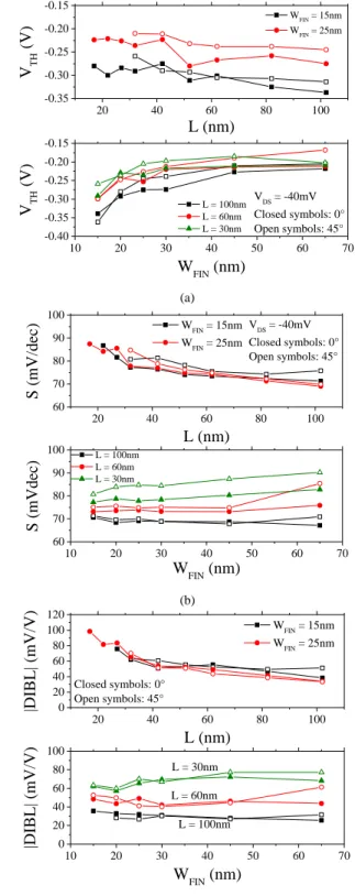
Fig. 5.a shows the VTH behavior with WFIN and L, extracted
by the second derivative method, at VDS = –40mV.
Improvements for narrower NWs and very small VTH roll-off
(lower than 60mV) is observed while reducing L down to 15nm. Figs. 5.b and 5.c show, respectively, S and |DIBL| results as a function of WFIN and L. A small subthreshold slope
degradation is obtained with channel shortening. For [110]-NWs with WFIN of 25nm, S is lower than 88mV/dec down to L
= 15nm. Through both S and |DIBL|, it is observed approximately constant dependence with WFIN for L = 100nm
and 60nm, reduced SCE for narrower NWs for L = 30nm and that both [110]- and [100]-NWs exhibit similar results, as predicted by the logarithmic scaled curves in Fig. 3. Besides, |DIBL| is lower than 100mV/V for [110]-oriented NWs with WFIN = 25nm and L down to 15nm.
Fig. 6 shows the results for the total resistance (RT =
VDS/IDS) as a function of the inverse of the NW gain (β), for
[110] and [100]-NWs, WFIN of 15, 30 and 65nm, VDS = –40mV
and VGT = –1V. From these curves, RS is extracted following
the Y-function method [12]. Good linearity of the data points is demonstrated by the solid lines, which lead to series resistance values around 140 and 360Ω.µm, for [110] and [100]-NWs, respectively. The linear curves observed in Fig. 6 cross the y-axis at the same RT.Weff value for all WFIN studied, indicating
that RS scales with WFIN for the entire range of L, from 100
down to 15nm.
The hole mobility as a function of the inversion carrier density (Ninv) extracted by split-CV technique [13] for L =
100nm and WFIN = 15nm is shown in Fig. 7. The maximum
mobility is found equal to 63 and 32cm2/V.s for standard and
rotated NWs, respectively. Moreover, the inner figure shows that the eff ratio between both [110] and [100]-NWs is close to
2, which agrees with the ION/Weff results obtained in Fig. 4.
Fig. 8 presents eff as a function of L (a), extracted by
Y-function method, and as a Y-function of WFIN (b), extracted by
split-CV technique, for several NWs, at Ninv of 0.8×1013cm-2.
Standard NWs show strong eff degradation for L < 60nm
while rotated NWs present a constant, but lower, mobility down to L = 30nm. Besides, eff shows improvements of up to
17% with WFIN reduction for [110]-NWs, while [100]-NWs
0 1 2 3 0.0 0.5 1.0 1.5 2.0 2.5 3.0 0 1 2 3 4 R S ~ 140.m Standard NWs Rotated NWs L from 15nm to 100nm VDS = -40mV and VGT = -1V W FIN = 15nm W FIN = 30nm W FIN = 65nm
R
T .W
eff(k
.m)
(a) (b) R S ~ 360.mR
T .W
eff(k
.m)
1/(
x
V
2/A)
Fig.6. RT.Weff as a function of 1/β for several [110] (a) and [100]-NWs (b),
at VDS = –40mV and VGT = –1V. 20 40 60 80 100 -0.35 -0.30 -0.25 -0.20 -0.15 10 20 30 40 50 60 70 -0.40 -0.35 -0.30 -0.25 -0.20 -0.15 VTH (V) L (nm) WFIN = 15nm WFIN = 25nm VDS = -40mV Closed symbols: 0° Open symbols: 45° VTH (V) WFIN (nm) L = 100nm L = 60nm L = 30nm (a) 20 40 60 80 100 60 70 80 90 100 10 20 30 40 50 60 70 60 70 80 90 100 VDS = -40mV Closed symbols: 0° Open symbols: 45° S (mV/dec ) L (nm) W FIN = 15nm W FIN = 25nm L = 100nm L = 60nm L = 30nm S (mVdec) W FIN (nm) (b) 20 40 60 80 100 0 20 40 60 80 100 120 10 20 30 40 50 60 70 0 20 40 60 80 100 Closed symbols: 0° Open symbols: 45° |DIBL| (mV/V) L (nm) WFIN = 15nm WFIN = 25nm L = 30nm L = 60nm L = 100nm |DIBL| (mV/V) WFIN (nm) (c)
Fig.5. VTH (a), S (b) and |DIBL| (c) as a function of both L and WFIN, for
0.0 0.5 1.0 1.5 2.0 0 10 20 30 40 50 60 70 80 90 0.0 0.5 1.0 1.5 2.0 0 1 2 3 4 VDS = -40mV WFIN = 15nm L = 100nm
eff(cm
2/V.s)
N
inv(x10
13cm
-2)
0°
45°
eff _ 0 ° / eff _ 4 5 ° Ninv (x1013 cm-2 )Fig.7. µeff and µeff_0°/µeff_45° as a function of Ninv for [110] and
[100]-NWs, L = 100nm and WFIN = 15nm, at VDS = –40mV. 20 40 60 80 100 10 20 30 40 50 20 40 60 10 20 30 40 50 60 L = 100nm 45° 0° Ninv = 0.8x1013 cm-2 VDS = -40mV eff (cm 2 /V.s) L (nm) (a) WFIN = 15nm WFIN = 25nm 45° 0° eff (cm 2 /V.s) WFIN (nm) (b) ~ 0% +17%
Fig.8. µeff as a function of L (a) and WFIN (b) for several [110] and [100]-NWs,
at Ninv = 0.8×1013cm-2 and VDS = –40mV.
show constant behavior, which is agreement with triple gate MOSFETs results [14].
IV. CONCLUSIONS
Two levels stacked NWs present high ION/WFIN (up to
2500µA/µm for [110]-NWs), although smaller µeff is expected
for stacked p-NWs in comparison to 3G MOSFETs due to stronger top surface (100) contribution.
Despite complex source and drain engineering, the small values of series resistance extracted for [110]-stacked NWs are comparable to those obtained for advanced planar MOSFETs.
Excellent SCE control (small VTH, S and DIBL
degradations down to 15nm gate length) have been obtained for both [110] and [100]-oriented NWs due to good electrostatic coupling and channel control provided by the sum of Ω-Gate and GAA wires.
On the same way as for 3G NWs, [110] orientation is better for p-type stacked NWs due to hole mobility improvements in (110)-oriented sidewalls.
ACKNOWLEDGMENTS
The authors would like to acknowledge the French Public Authorities from NANO 2017 program, CNPq and São Paulo Research Foundation (FAPESP) grants 2015/10491-7 and 2016/06301-0.
This work is also partially funded by the SUPERAID7 (grant N° 688101) project.
REFERENCES
[1] J.-P. Colinge, “Multiple-gate SOI MOSFETs,” Solid-State Electron., vol. 48, no. 6, pp. 897–905, Jun. 2004.
[2] K. J. Kuhn, “Considerations for Ultimate CMOS Scaling,” IEEE
Trans. Electron Devices, vol. 59, no. 7, pp. 1813–1828, Jul. 2012.
[3] R. Coquand et al., “Strain-induced performance enhancement of tri-gate and omega-tri-gate nanowire FETs scaled down to 10nm Width,” in
2012 Symposium on VLSI Technology (VLSIT), 2012, pp. 13–14.
[4] R. Coquand et al., “Scaling of high-k/metal-gate Trigate SOI nanowire transistors down to 10nm width,” in 2012 13th International
Conference on Ultimate Integration on Silicon (ULIS), 2012, pp. 37–
40.
[5] S. Barraud et al., “Strained Silicon Directly on Insulator N- and P-FET nanowire transistors,” in 2014 15th International Conference on
Ultimate Integration on Silicon (ULIS), 2014, pp. 65–68.
[6] M. Saitoh et al., “Short-channel performance and mobility analysis of <110>- and <100>-oriented tri-gate nanowire MOSFETs with raised source/drain extensions,” in 2010 Symposium on VLSI Technology, 2010, pp. 169–170.
[7] H. Mertens et al., “Gate-all-around MOSFETs based on vertically stacked horizontal Si nanowires in a replacement metal gate process on bulk Si substrates,” in 2016 IEEE Symposium on VLSI Technology, 2016, pp. 1–2.
[8] C. Dupre et al., “15nm-diameter 3D stacked nanowires with independent gates operation: ΦFET,” in 2008 IEEE International
Electron Devices Meeting, 2008, pp. 1–4.
[9] S. Barraud et al., “Vertically stacked-NanoWires MOSFETs in a replacement metal gate process with inner spacer and SiGe source/drain,” in 2016 IEEE International Electron Devices Meeting
(IEDM), 2016, p. 17.6.1-17.6.4.
[10] S. Takagi, A. Toriumi, M. Iwase, and H. Tango, “On the universality of inversion layer mobility in Si MOSFET’s: Part II-effects of surface orientation,” IEEE Trans. Electron Devices, vol. 41, no. 12, pp. 2363– 2368, Dec. 1994.
[11] J. Pelloux-Prayer et al., “Study of the piezoresistive properties of NMOS and PMOS Ω-gate SOI nanowire transistors: Scalability effects and high stress level,” in Electron Devices Meeting (IEDM),
2014 IEEE International, 2014, p. 20.5.1-20.5.4.
[12] G. Ghibaudo, “New method for the extraction of MOSFET parameters,” Electron. Lett., vol. 24, no. 9, pp. 543–545, Apr. 1988. [13] A. Ohata, M. Cassé, and S. Cristoloveanu, “Front- and back-channel
mobility in ultrathin SOI-MOSFETs by front-gate split CV method,”
Solid-State Electron., vol. 51, no. 2, pp. 245–251, Feb. 2007.
[14] J. Pelloux-Prayer et al., “Transport in TriGate nanowire FET: Cross-section effect at the nanometer scale,” in 2016 IEEE
SOI-3D-Subthreshold Microelectronics Technology Unified Conference (S3S),
![Fig. 3 presents the normalized drain current (I DS .L) as a function of the gate voltage (V GS ) for [110] (0°) and [100]](https://thumb-eu.123doks.com/thumbv2/123doknet/12979036.378191/3.893.62.426.79.373/fig-presents-normalized-drain-current-function-gate-voltage.webp)