HAL Id: cea-01546754
https://hal-cea.archives-ouvertes.fr/cea-01546754
Submitted on 26 Jun 2017HAL is a multi-disciplinary open access archive for the deposit and dissemination of sci-entific research documents, whether they are pub-lished or not. The documents may come from teaching and research institutions in France or abroad, or from public or private research centers.
L’archive ouverte pluridisciplinaire HAL, est destinée au dépôt et à la diffusion de documents scientifiques de niveau recherche, publiés ou non, émanant des établissements d’enseignement et de recherche français ou étrangers, des laboratoires publics ou privés.
Distributed under a Creative Commons Attribution - NonCommercial| 4.0 International License
Localized electrochemistry for the investigation and the
modification of 2D materials
Kevin Jaouen, Olivier Henrotte, Stéphane Campidelli, Bruno Jousselme,
Vincent Derycke, Renaud Cornut
To cite this version:
Kevin Jaouen, Olivier Henrotte, Stéphane Campidelli, Bruno Jousselme, Vincent Derycke, et al.. Lo-calized electrochemistry for the investigation and the modification of 2D materials. Applied Materials Today, Elsevier, 2017, 8, pp.116 - 124. �10.1016/j.apmt.2017.05.001�. �cea-01546754�
1
Localized electrochemistry for the investigation and
the modification of 2D materials
K. Jaouen, O. Henrotte, S. Campidelli, B. Jousselme, V. Derycke, R. Cornut*
LICSEN, NIMBE, CEA, CNRS, Université Paris-Saclay, CEA Saclay 91191 Gif-sur-Yvette Cedex, France. E-mail: renaud.cornut@cea.fr
Abstract
In this review, we present the state of the art regarding the interplay between two emerging fields, namely localized electrochemistry and 2D materials. Electrochemistry involves oxidations and reductions taking place at an electrode immersed in a solution. When the substrate is composed of 2D materials or layered materials, electrochemistry can be used to investigate or modify these layers. It is thus an essential link between 2D materials and their applications, in particular those related to sustainable energy conversion and storage. In addition, the properties of 2D materials often differ along their edges, at defect sites or upon folding and stacking. Most interesting properties (such as catalytic activity, conductivity, chemical reactivity, etc.) drastically depend on such inhomogeneity or imperfections, which can be purposely induced (by functionalization or nanostructuration) or not (intrinsic defects resulting from the material synthesis or consequences of the material handling and deposition processes). These key aspects are suitably investigated using local electrochemical strategies, which allow both the analysis and the local modification of 2D materials. This article reviews the most significant results of this rapidly growing field.
Introduction
2D materials are foreseen as key building blocks in an increasing number of applications ranging from electronics to energy storage and conversion devices. Since Novoselov et al. isolated single-layer graphene by simple mechanical exfoliation in 20041 the fabrication of 2D materials has made very rapid progresses, and the community has now access to a wide variety of 2D materials with many different properties. They can be derived from graphene (graphene oxide, few layer graphene, etc)2 or contain transition metal dichalcogenides.3 However, while 2D materials already lead to performance improvement in several examples4 (electrocatalysis,5 optoelectronics,6 etc), the understanding of the precise origin of such improvement remains challenging. In fact the integration of new materials into functional devices critically relies on our ability to both understand and modify their intrinsic properties. In this regard, the study of the interface of two systems (e.g. 2D materials and ionic solutions) to investigate electron transfer implying oxidation-reduction reactions known as “electrochemistry” appears particularly appealing to analyze new 2D layers and improve their functionality. It must be noticed that in devices, global performances are the result of many contributions coming from different elements present in the functional layer. In fact, the inherent heterogeneity (edges, folds, defects, stacks...) of the deposited 2D materials is both a chance –as the particular properties of the modified surface are often due to such heterogeneities– and a challenge –as their analysis or modification require local investigations.
2
There are two main strategies to explore the electrochemical properties of 2D materials and relate them to local information. The first one consists in performing standard electrochemistry on substrates having variable and identified amounts (or percentage) of specific features under investigation (edges, planes, stacks, etc). This requires complementary experiments using conventional characterization tools (Atomic Force Microscopy (AFM), Scanning Electron Microscopy, (SEM)…). An alternative and particularly powerful approach relies on electrochemical scanning probe techniques. In this case, an electrode (such as a functional AFM cantilever, a microelectrode or a pipette, see below) is used as local probe and moved over the substrates to provide an electrochemical map of the substrate. Depending on the scanning conditions different information can be obtained. In this review, we start by presenting the different local probe techniques that can be used to perform localized electrochemical investigations of 2D materials. Then, we present the studies in which localized electrochemistry experiments are used to evaluate some key properties of 2D materials. Finally, in a last part, we focus on contributions related to material modifications (electrochemical functionalization, etching…), which allow modulation of the properties in a spatially controlled manner.
1. Local probe techniques
To combine electrochemistry and micrometric or submicrometric investigations, the most common strategy is to use a small probe and displace it in the vicinity of the materials. Depending on the type of probe, different techniques are considered.
The most common technique to perform local electrochemistry uses a microdisk electrode, i.e. a metallic wire surrounded by an insulator as schematically illustrated in figure 1a. In this case, the local probe technique is named “Scanning Electrochemical Microscopy” abbreviated as SECM.7 Introduced in 1989, the technique combines a standard electrochemistry set up (three-electrode system) with motors and positioning systems to move the probe which can be micro- to nano-sized. The probe is usually the working electrode in the electrochemical set up, which means that both the current and the potential are accessible experimentally. The size of the probe determines the spatial resolution of the study that ranges typically from 10 µm to 1 µm. With a bipotensiostat, it is possible to monitor the electric potentials of both the substrate and the tip. The SECM configuration offers a large variety of electrochemical characterizations through the change of the experimental sequences such as the probe and substrate potentials, or the electrolyte content.8 Electrochemical measurements can also be
combined with Atomic Force Microscopy in a combined AFM-SECM approach (Fig. 1b) to get simultaneously topological and electrochemical information.9 This permits the deconvolution of the two contributions and a more precise evaluation of the electrochemical activity. Another technique derived from SECM known as Scanning ElectroChemical Cell Microscopy (SECCM) consists of a dual-channel pipette with a Quasi-Counter-Reference Electrode (QCRE) in each channel with a fixed potential bias between both (Fig. 1c).10 Only the probe is filled with solution so that only the area of interest is analyzed. When the solution is confined with a micropipette, the technique is called “microdroplet cell” (Fig. 1d) and micrometric spatial resolution can be achieved.11
3
Figure 1. Presentation of the different probe techniques to perform localized electrochemistry (a) SECM, (b) AFM-SECM, (c) SECCM, (d) Microdroplet cell. WE: Working Electrode, CE: Counter Electrode, RE: Reference Electrode, QCRE: Quasi Counter Reference Electrode. The green triangle represents a piece of 2D material under study.
2. Characterization of electronic transfers
Most of the time, the source of the measured probe signal is unambiguously identified thanks to concordant non-electrochemical images, generally obtained by SEM, AFM or spectroscopy (see examples below). In the following part, different investigations of 2D materials are reviewed. In a first section, the investigations dealing with simple electron transfers between the layer and a redox mediator present in the electrolyte solution, such as ferrocene, are presented. The charge transfer kinetic associated to these simple processes informs on the ability of the 2D layer to exchange electrons with its environment. In a second section, the studies of more complex reactions (involving multistep mechanisms and absorbed species) are reviewed. Finally, the investigations of the transport of species (electrons, absorbed species, etc.) within or on top of the layer(s) are presented.
2.1. Redox mediator charge transfers
First, local electrochemistry is used to investigate how simple charge transfers occur at surfaces covered with layered materials, with a special focus on graphene. In this
4
configuration, the probe is used as an electrode to extract or bring electrons to these materials, through the solution that contains a redox mediator such as typically Fe(CN)63- or Ferrocene.
Local electrochemistry is perfectly suitable to investigate the impact of defects and edges on electronic transfers. In fact, such investigation of layered materials follows extensive studies on bulk materials exhibiting crystalline surfaces.12 In particular, highly oriented pyrolytic graphite (HOPG) has been extensively investigated.12c Using standard electrochemistry12b, 13 or local probes14 structural defects (see figure 2) are identified as more efficient locations for
electron exchanges between the solution and the surface. The effective activity of graphite basal plane is also the subject of intense debates.15 SECCM shows that basal planes can effectively exchange electrons with a solution,16 even when Fe(CN)
63- is used as redox
mediator, which is well known to have a low charge transfer kinetic.
How these conclusions are transferable from HOPG to 2D materials is also investigated. This is done either with local probes9c, 17 or surface templating.18 It is
concluded that charge transfer is more favorable on graphene than on HOPG: both the defects17b, 18a, b and the basal plane18c have a higher activity on graphene than on HOPG. Different redox mediators are considered, and small kinetic constants for Fe(CN)63- and higher constants for ferrocene are observed.19 These observations
are in line with the previously mentioned studies dealing with HOPG. The importance of folding effects at graphene edges is also investigated by electrochemistry. It shows that the charge transfer is about 35 times faster at open-edged than at folded-edges.20 The number of layers also impacts the charge transfer constants: conversely to what can be expected from the difference between bulk materials and monolayers, with graphene11, 21 or MoS222 the general
trend is to observe an enhanced charge transfer upon increasing the number of layers, as illustrated in figure 3. Quantitative studies show that the charge transfer kinetics (with FeCN63- and IrCl62-) on graphene approximately double when going from 1 to 2 layers.23 With
2D materials, the surface underneath the layer impacts the transfer kinetics, for example by trapping charges in the vicinity of the 2D materials, thereby screening part of the applied potential.24 Gold subsurface also enhances the charge transfer by a factor of about 5 due to
electronic coupling between the layer and the gold.25 The high sensitivity of the charge transfer to the sublayer and to the redox mediator is similarly observed on graphene oxide (GO) and on reduced graphene oxide (r-GO).26
Figure 2. Schematic view of the graphite surface and examples of local sites with potentially different electrochemical activity
5
Figure 3. Microscopy of exfoliated graphene on a Si/SiO2 substrate. (a) Optical microscopy
image (dashed lines define the boundaries between the graphene sample and the substrate), (b) AFM topographical image, and (c) SECCM map for the reduction of Ru(NH3)63+.
Reprinted with permission from 21b. The areas identified as dotted rectangles in figure b have lower SECCM response in figure c.
2.2. Electrocatalysis
The growing role of layered materials in energy storage and conversion devices5b makes the understanding of their electrocatalytic properties of paramount importance. This is notably the case for the Oxygen Reduction Reaction (ORR) and Hydrogen Evolution Reaction (HER) encountered in fuel cells and electrolyzers.5a Only few studies of ORR catalysis on 2D materials are presently available. With a microdroplet cell, ORR on HOPG is observed as being more efficient on edges than on basal planes27 similarly as for simpler charge transfers.
ORR performances of MoSe2 and r-GO hybrid nanostructures are evaluated with SECM,
providing direct evidence of the synergy between both components.28
Figure 4. (a) Illustrative STM image (47 nm x 47nm) of MoS2 on Au(111). Exchange current
density regarding H2 evolution versus MoS2 area coverage (b) and MoS2 edge length (c). A
strong linear correlation is only observed in the latter case. Open and filled circles correspond to different annealing temperatures of the samples (400 and 550°C respectively). Reprinted with permission from 29.
6
HER is very much investigated on MoS2.30 The enhanced activity of edges is observed with
substrates covered by MoS2 flakes having different sizes, which generate different edge
contents on the samples (figure 4).29 The enhanced activity of edges is also observed on macroscopic MoS2 crystals having basal or edge exposed planes.12b Studied with SECM,
sulfur vacancies within the plane are found to enhance the kinetic constants by a factor of 4 if the structure is strained,31 while the surface coverage of adsorbed H2 at the surface increases
when decreasing the substrate potential.32
Figure 5. Investigation of 2D materials using the interface between 2 immiscible electrolyte solutions. (a) Scheme of the process for HER assessment, (b) The UV-vis cell used to follow the reaction, (c) Experimental results showing that MoS2 on mesoporous carbon has the
highest activity. Reprinted with permission from 33.
At the border of the scope of this review dealing with localized electrochemistry, it is worth mentioning that the electrocatalytic activity of MoS2 toward HER can also be investigated by
trapping 2D layers at the interface between 2 immiscible electrolyte solutions, as presented in figure 5. The activity toward HER is studied by biphasic reactions monitored by UV/Vis spectroscopy. The presence of MoS2 edges and the strong electronic coupling between the
MoS2 and the support leads to enhanced performances. 33 Surprisingly few studies perform
localized electrochemistry to investigate the photocatalytic activity of 2D materials. Scanning photocurrent microscopy34, which uses a laser beam focused on the surface (figure 6a) and
evaluates the generated current at the substrate to map the quantum yield of a sample with micrometric lateral resolution. With this technique, the photoproduction of H2 by Pt
nanoparticles deposited on WSe2 layersis observed to be very heterogeneous along the crystal
(figure 6b-c).35 Such strategy perfectly matches the ongoing increasing complexity of the photocatalytic systems. A rapid growth of the utilization of scanning photocurrent microscopy can thus be anticipated in the next years.
7
Figure 6. (a) Principle of Scanning photocurrent microscopy applied to the investigation of Pt-WSe2. Example of combined SEM (b) and quantum yield map (c) obtained in the presence
of Ru(NH3)63+. Reprinted with permission from 35 .
2.3. Electrons, ions and molecules transport on surfaces
In sections 2.1 and 2.2, the mentioned studies are related to charge transfers occurring perpendicularly to the layers, from the material to the electrolyte. Local measurements also permit to investigate the transport of molecules, ions or electrons parallel to the surface. Electronic
transport on r-GO flakes is
investigated with SECM, as illustrated in figure 7. The measurement provides information on the local conductivity of the substrate via a feedback loop between the probe and the flake (figure 7d). Both the intrinsic conductivity36 (measured on individual flakes) and the contact resistance37 between r-GO flakes (evaluated on perfectly identified flake-flake junctions within small aggregates) can be quantified. The measurements show that when the GO flakes are reduced with hydroiodic acid (HI),38 the contact resistance is 5 times larger than the flake resistance. The macroscopic resistance of r-GO thin films is thus mostly governed by contacts between flakes.
Figure 7. Micrographs of the same r-GO flake deposited on Si/SiO2 wafer. (a) SEM image, (b) AFM image and (c)
SECM image obtained using Ferrocene as redox mediator. (d) Scheme presenting the different steps involved in the feedback loop between the probe and the microelectrode during SECM measurements. Reprinted with permission from 60.
8
Concerning the transport of molecules, surface diffusion on graphene of a tripodal cobalt complex was investigated with SECM.39 The technique permits to observe the evolution of a spot of molecules deposited on the layer, by measuring its hindering effect on the charge transfer between the graphene and the solution. By surface diffusion, the surface concentration decreases and the exchange of electrons between the graphene and the solution is reactivated. With this strategy, the diffusion is measured to be slower on graphene than in solution, but faster than in solids. Concerning the transport of ions, the Li+ intercalation
within few layer graphene was investigated. Electrochemistry coupled to Raman spectroscopy40 shows the increase of strain upon intercalation when decreasing the number of layers. SECM (using a Hg-capped microelectrode, see41 for more details) on purposely
templated substrates concludes that Li ions move into graphene interlayers more efficiently through the edge planes.42 Li intercalation within MoS2 was followed with Raman
spectroscopy and in situ optical observations.43 The study shows how the optical transmission and the electronic conductivity of the layers are impacted by the intercalation process.
To conclude on this part, many of the technical difficulties associated to localized electrochemical analysis of 2D materials have now been overcome, and many protocols to investigate a precise process on a given layer are now available. The observed features depend on the observation scale: as an illustration, nanometric artifacts do not have an observable signature if micrometric probes are used. This is for example the case in figure 7, where AFM and SEM show flake folding that is not observed with SECM performed with a 10 µm diameter microelectrode. The next step is now to use the methods on series of 2D materials in order to improve the understanding of these systems. This is particularly the case in electrocatalysis, where the diversity of situations, the sensitivity of the processes to defects and the complexity of the mechanisms perfectly match the versatility of localized electrochemistry. Besides, it can be noticed that some 2D materials exist under different phases (1T and 2H for MoS2). 44 These have very different electronic and optic properties, and
this could be advantageously studied by localized electrochemistry. At the present moment, we do not have knowledge of such studies.
3. Material modification
Localized electrochemistry is also used to modify locally 2D materials with a spatial resolution mainly limited by the probe size. This is a highly versatile alternative to template-based strategies such as photolithography. Probe-induced surface modification is very popular for other materials than 2-dimensional ones.45 Regarding the modification of 2D materials, as
detailed in the following, the existing works mainly deal with graphene or graphene derivatives such as GO, so that many routes for the modification of other 2D materials are not explored yet.
3.1. Localized oxidation of 2D materials
The scientific community has been working on the probe-induced modification of graphene since 2008.46 Most of the studies use a well-known technique, Local Anodic Oxidation (LAO), which was introduced in 1989 for creating holes on graphite surface with an STM.47 The electrochemical nature of the process was identified soon after, as illustrated in figure 8a.48
9
Figure 8. (a) Principle of local anodic oxidation (LAO) on graphene with an AFM. Reprinted with permission from46a. (b-c) AFM images of a graphene flake before (b) and after (c) LAO.
The cut follows the yellow dashed arrow. (d-e) AFM (d) and height profile (e) showing that trenches or bumps can be created on graphene by LAO. Reprinted with permission from 46b.
With graphene, most studies employ conductive AFM (C-AFM) both in contact or tapping mode. Different degrees of modifications of graphene can be achieved by oxidation leading to either GO formation or surface etching.46 As illustrated in Figure 8(c-d), etching leads to trenches while oxidation leads to bumps. 46b At high voltage, low scanning speed favors etching.49 By optimizing the LAO conditions graphene nano-constrictions as small as 10 nm can be fabricated.50 It should be noted that only two localized oxidation studies of other materials were reported, both using an AFM tip as patterning probe. The first one describes the patterning of semiconducting TaS2 layers leading to the formation of insulating Ta2O5
regions51 while the second one describes the patterning of semiconducting MoS2 layers
leading to the formation of insulating MoOxSy regions.52
3.2. Localized reduction of 2D Materials
Compared to oxidation, local reduction of 2D materials is hardly studied. Similarly as for oxidation with LAO, C-AFM can be used. Most of the time, the goal is to locally reduce GO to restore some electrical conductivity.53 One study notably shows that the localized reduction of GO can be used to pattern the channel of ambipolar field-effect transistors.54 Soon after it
was found that humidity and the number of layers have an important impact on the spatial resolution of this reduction process, and that generation and transport of protons limit the reaction kinetics.55 Unlike oxidation, other methods than STM and AFM can be used to
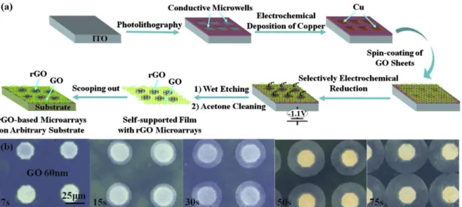
locally reduce 2D materials. By combining photolithography, electrochemical reduction and wet etching techniques, r-GO microarrays where fabricated,56 as shown in figure 9.
10
Figure 9. Process combining micropatterning and electrochemistry to reduce locally GO. (a) Overview of the process (b) Laser microscopy images showing the pattern size obtained for different electrochemical reductions durations. Reprinted with permission from 56.
Microelectrodes in a SECM configuration are also used to locally reduce GO by electrogenerated naphthalene radical anions, as shown in figure 10.57 Both the chemical composition of the layer and the electrical conductivity are modified during the process, as shown in figure 10b and 10c, respectively.57
Figure 10. Localized reduction of GO with naphthalene radical anions generated by a negatively polarized microelectrode. (a) Scheme of the procedure (b) XPS data (C1s and O1s core levels) on GO and after SECM-induced reduction in r-GO. (c) SEM image of an r-GO line (within a GO thin film) connected to gold electrodes. Reprinted with permission from 57.
3.3. Functionalization of 2D materials
Local electrochemistry is also used to perform more complex transformations. After reduction of GO, the increased conductivity of the r-GO motifs can be used to perform localized diazonium electrografting.57 Diazonium functionalization is a well-known reaction on sp2 carbon materials58 that was also performed on HOPG with SECCM.59 Local carboxylation of
multilayered graphene is demonstrated with an SECM, as shown in figure 11.60 It demonstrates that the degree of modification can be controlled by the electrolysis duration.
11
Figure 11. CO2 functionalization of graphene with SECM. (a) Scheme presenting the strategy.
(b) SECM image obtained after reduction, showing a decrease in the ability of the functionalized zones to exchange charges with the solution, due to the presence of the CO2
moieties. Reprinted with permission from 60.
Another approach uses 2D layers placed at the interface between two immiscible liquids, as already presented in figure 4, to perform electrodeposition of an inorganic compound selectively at one side of the 2D material.61 Alternatively, the 2D layers can be deposited on a sacrificial substrate that undergoes oxidation upon electrodeposition.62 These strategies lead to Janus types of 2D materials having promising electrocatalytic activities toward HER.
To conclude on this part, literature shows that the diversity of surface modifications with conventional electrochemistry can in most cases be transferred into local modifications. The main challenges of this field are to improve the spatial resolution and to generate more complex patterns while limiting the modification time. Surface modification can also be an interesting support for surface reactivity analysis as for example in reference 15c, where the adsorption on HOPG of an anthraquinone derivative is used to show that edges do not present an enhanced electrochemical activity.
Conclusion
Utilization of local electrochemistry for analysis, patterning or functionalization of 2D materials is a rapidly growing field. At the present stage, most of the reported studies focus on graphene or analogues such as graphene oxide and reduced graphene oxide, and the most typical characterization concerns the evaluation of the kinetic constant associated to simple charge transfers. From this basis, much needs to be done in order to better understand 2D materials thanks to localized electrochemistry. This is particularly the case as the relatively recent utilization of other 2D materials than graphene gives unprecedented access to original properties, which opens new research directions and generates new needs in terms of characterization, understanding and modification. As an illustration, the photochemical properties of dichalcogenides are particularly promising in photocatalysis, but several fundamental studies regarding the underlying processes are still missing. These would combine local electrochemistry with spectroscopy and other microscopy techniques. Besides, it should be noted that only a very limited number of studies combine local electrochemistry experiments with numerical simulations. Such combination could drastically increase the outcomes by enabling a quantitative interpretation of the measurements. In any case, localized electrochemistry has the potentiality to cover many needs for analysis and modification of 2D materials and thus to provide information and solutions of particular relevance for future devices and applications.
12
This work was supported by a public grant overseen by the French National Research Agency (ANR) as part of the “Investissements d’Avenir” program (Labex NanoSaclay, reference: ANR-10-LABX-0035).
1. Novoselov, K. S.; Geim, A. K.; Morozov, S. V.; Jiang, D.; Zhang, Y.; Dubonos, S. V.; Grigorieva, I. V.; Firsov, A. A., Electric field effect in atomically thin carbon films. Science 2004, 306 (5696), 666-669.
2. Zhu, Y. W.; Murali, S.; Cai, W. W.; Li, X. S.; Suk, J. W.; Potts, J. R.; Ruoff, R. S., Graphene and Graphene Oxide: Synthesis, Properties, and Applications. Adv. Mater. 2010, 22 (35), 3906-3924. 3. Reale, F.; Sharda, K.; Mattevi, C., From bulk crystals to atomically thin layers of group VI-transition metal dichalcogenides vapour phase synthesis. Applied Materials Today 2016, 3, 11-22. 4. Butler, S. Z.; Hollen, S. M.; Cao, L.; Cui, Y.; Gupta, J. A.; Gutiérrez, H. R.; Heinz, T. F.; Hong, S. S.; Huang, J.; Ismach, A. F.; Johnston-Halperin, E.; Kuno, M.; Plashnitsa, V. V.; Robinson, R. D.; Ruoff, R. S.; Salahuddin, S.; Shan, J.; Shi, L.; Spencer, M. G.; Terrones, M.; Windl, W.; Goldberger, J. E., Progress, Challenges, and Opportunities in Two-Dimensional Materials Beyond Graphene. ACS Nano 2013, 7 (4), 2898-2926.
5. (a) Zhu, C.; Dong, S., Recent progress in graphene-based nanomaterials as advanced electrocatalysts towards oxygen reduction reaction. Nanoscale 2013, 5 (5), 1753-1767; (b) Bonaccorso, F.; Colombo, L.; Yu, G.; Stoller, M.; Tozzini, V.; Ferrari, A. C.; Ruoff, R. S.; Pellegrini, V., Graphene, related two-dimensional crystals, and hybrid systems for energy conversion and storage.
Science 2015, 347 (6217).
6. Georgiou, T.; Jalil, R.; Belle, B. D.; Britnell, L.; Gorbachev, R. V.; Morozov, S. V.; Kim, Y.-J.; Gholinia, A.; Haigh, S. J.; Makarovsky, O.; Eaves, L.; Ponomarenko, L. A.; Geim, A. K.; Novoselov, K. S.; Mishchenko, A., Vertical field-effect transistor based on graphene-WS2 heterostructures for flexible and transparent electronics. Nat Nano 2013, 8 (2), 100-103.
7. (a) Amemiya, S.; Bard, A. J.; Fan, F. R. F.; Mirkin, M. V.; Unwin, P. R., Scanning Electrochemical Microscopy. Annu. Rev. Anal. Chem. 2008, 1, 95-131; (b) Mirkin, M. V.; Nogala, W.; Velmurugan, J.; Wang, Y. X., Scanning Electrochemical Microscopy in the 21st century. Update 1: Five Years After.
Phys. Chem. Chem. Phys. 2011, 13 (48), 21196-21212; (c) Amemiya, S.; Chen, R.; Nioradze, N.; Kim, J.,
Scanning Electrochemical Microscopy of Carbon Nanomaterials and Graphite. Accounts of Chemical
Research 2016, 49 (9), 2007-2014; (d) Bard, A. J.; Fan, F. R. F.; Kwak, J.; Lev, O., Scanning
electrochemical microscopy. Introduction and principles. Anal. Chem. 1989, 61 (2), 132-138; (e) Engstrom, R. C.; Pharr, C. M., Scanning Electrochemical Microscopy. Anal. Chem. 1989, 61 (19), 1099A-1104.
8. (a) Lefrou, C.; Cornut, R., Analytical Expressions for Quantitative Scanning Electrochemical Microscopy (SECM). ChemPhysChem 2010, 11 (3), 547-556; (b) Polcari, D.; Dauphin-Ducharme, P.; Mauzeroll, J., Scanning Electrochemical Microscopy: A Comprehensive Review of Experimental Parameters from 1989 to 2015. Chem. Rev. 2016, 116 (22), 13234-13278.
9. (a) Macpherson, J. V.; Unwin, P. R.; Hillier, A. C.; Bard, A. J., In-Situ Imaging of Ionic Crystal Dissolution Using an Integrated Electrochemical/AFM Probe. J. Am. Chem. Soc. 1996, 118 (27), 6445-6452; (b) Macpherson, J. V.; Unwin, P. R., Combined Scanning Electrochemical−Atomic Force Microscopy. Anal. Chem. 2000, 72 (2), 276-285; (c) Wain, A. J.; Pollard, A. J.; Richter, C., High-Resolution Electrochemical and Topographical Imaging Using Batch-Fabricated Cantilever Probes.
Anal. Chem. 2014, 86 (10), 5143-5149.
10. (a) Lai, S. C. S.; Dudin, P. V.; Macpherson, J. V.; Unwin, P. R., Visualizing Zeptomole (Electro)Catalysis at Single Nanoparticles within an Ensemble. J. Am. Chem. Soc. 2011, 133 (28), 10744-10747; (b) Ebejer, N.; Schnippering, M.; Colburn, A. W.; Edwards, M. A.; Unwin, P. R., Localized High Resolution Electrochemistry and Multifunctional Imaging: Scanning Electrochemical Cell Microscopy. Anal. Chem. 2010, 82 (22), 9141-9145.
13
11. (a) Toth, P. S.; Valota, A. T.; Velicky, M.; Kinloch, I. A.; Novoselov, K. S.; Hill, E. W.; Dryfe, R. A. W., Electrochemistry in a drop: a study of the electrochemical behaviour of mechanically exfoliated graphene on photoresist coated silicon substrate. Chem. Sci. 2014, 5 (2), 582-589; (b) Velický, M.; Bradley, D. F.; Cooper, A. J.; Hill, E. W.; Kinloch, I. A.; Mishchenko, A.; Novoselov, K. S.; Patten, H. V.; Toth, P. S.; Valota, A. T.; Worrall, S. D.; Dryfe, R. A. W., Electron Transfer Kinetics on Mono- and Multilayer Graphene. ACS Nano 2014, 8 (10), 10089-10100.
12. (a) Velicky, M.; Bissett, M. A.; Toth, P. S.; Patten, H. V.; Worrall, S. D.; Rodgers, A. N. J.; Hill, E. W.; Kinloch, I. A.; Novoselov, K. S.; Georgiou, T.; Britnell, L.; Dryfe, R. A. W., Electron transfer kinetics on natural crystals of MoS2 and graphite. Phys. Chem. Chem. Phys. 2015, 17 (27), 17844-17853; (b) Tan, S. M.; Ambrosi, A.; Sofer, Z.; Huber, Š.; Sedmidubský, D.; Pumera, M., Pristine Basal- and Edge-Plane-Oriented Molybdenite MoS2 Exhibiting Highly Anisotropic Properties. Chem. Eur. J. 2015, 21 (19), 7170-7178; (c) McCreery, R. L., Advanced Carbon Electrode Materials for Molecular Electrochemistry. Chem. Rev. 2008, 108 (7), 2646-2687.
13. (a) McDermott, M. T.; Kneten, K.; McCreery, R. L., Anthraquinonedisulfonate adsorption, electron-transfer kinetics, and capacitance on ordered graphite electrodes: the important role of surface defects. The Journal of Physical Chemistry 1992, 96 (7), 3124-3130; (b) Davies, T. J.; Hyde, M. E.; Compton, R. G., Nanotrench Arrays Reveal Insight into Graphite Electrochemistry. Angewandte
Chemie International Edition 2005, 44 (32), 5121-5126.
14. Anne, A.; Cambril, E.; Chovin, A.; Demaille, C.; Goyer, C., Electrochemical Atomic Force Microscopy Using a Tip-Attached Redox Mediator for Topographic and Functional Imaging of Nanosystems. ACS Nano 2009, 3 (10), 2927-2940.
15. (a) Edwards, M. A.; Bertoncello, P.; Unwin, P. R., Slow Diffusion Reveals the Intrinsic Electrochemical Activity of Basal Plane Highly Oriented Pyrolytic Graphite Electrodes. J. Phys. Chem. C 2009, 113 (21), 9218-9223; (b) Williams, C. G.; Edwards, M. A.; Colley, A. L.; Macpherson, J. V.; Unwin, P. R., Scanning Micropipet Contact Method for High-Resolution Imaging of Electrode Surface Redox Activity. Anal. Chem. 2009, 81 (7), 2486-2495; (c) Zhang, G.; Kirkman, P. M.; Patel, A. N.; Cuharuc, A. S.; McKelvey, K.; Unwin, P. R., Molecular Functionalization of Graphite Surfaces: Basal Plane versus Step Edge Electrochemical Activity. J. Am. Chem. Soc. 2014, 136 (32), 11444-11451. 16. (a) Lai, S. C. S.; Patel, A. N.; McKelvey, K.; Unwin, P. R., Definitive Evidence for Fast Electron Transfer at Pristine Basal Plane Graphite from High-Resolution Electrochemical Imaging. Angewandte
Chemie International Edition 2012, 51 (22), 5405-5408; (b) Patel, A. N.; Collignon, M. G.; O’Connell,
M. A.; Hung, W. O. Y.; McKelvey, K.; Macpherson, J. V.; Unwin, P. R., A New View of Electrochemistry at Highly Oriented Pyrolytic Graphite. J. Am. Chem. Soc. 2012, 134 (49), 20117-20130.
17. (a) Unwin, P. R.; Güell, A. G.; Zhang, G., Nanoscale Electrochemistry of sp2 Carbon Materials: From Graphite and Graphene to Carbon Nanotubes. Accounts of Chemical Research 2016, 49 (9), 2041-2048; (b) Tan, C.; Rodríguez-López, J.; Parks, J. J.; Ritzert, N. L.; Ralph, D. C.; Abruña, H. D., Reactivity of Monolayer Chemical Vapor Deposited Graphene Imperfections Studied Using Scanning Electrochemical Microscopy. ACS Nano 2012, 6 (4), 3070-3079; (c) Zhong, J.-H.; Zhang, J.; Jin, X.; Liu, J.-Y.; Li, Q.; Li, M.-H.; Cai, W.; Wu, D.-Y.; Zhan, D.; Ren, B., Quantitative Correlation between Defect Density and Heterogeneous Electron Transfer Rate of Single Layer Graphene. J. Am. Chem. Soc. 2014,
136 (47), 16609-16617; (d) Patten, H. V.; Velicky, M.; Clark, N.; Muryn, C. A.; Kinloch, I. A.; Dryfe, R. A.
W., Electrochemistry of well-defined graphene samples: role of contaminants. Faraday Discussions 2014, 172 (0), 261-272.
18. (a) Yuan, W.; Zhou, Y.; Li, Y.; Li, C.; Peng, H.; Zhang, J.; Liu, Z.; Dai, L.; Shi, G., The edge- and basal-plane-specific electrochemistry of a single-layer graphene sheet. Scientific Reports 2013, 3, 2248; (b) Banerjee, S.; Shim, J.; Rivera, J.; Jin, X.; Estrada, D.; Solovyeva, V.; You, X.; Pak, J.; Pop, E.; Aluru, N.; Bashir, R., Electrochemistry at the Edge of a Single Graphene Layer in a Nanopore. ACS
Nano 2013, 7 (1), 834-843; (c) Li, W.; Tan, C.; Lowe, M. A.; Abruña, H. D.; Ralph, D. C.,
Electrochemistry of Individual Monolayer Graphene Sheets. ACS Nano 2011, 5 (3), 2264-2270.
19. Ritzert, N. L.; Rodríguez-López, J.; Tan, C.; Abruña, H. D., Kinetics of Interfacial Electron Transfer at Single-Layer Graphene Electrodes in Aqueous and Nonaqueous Solutions. Langmuir 2013,
14
20. Ambrosi, A.; Bonanni, A.; Pumera, M., Electrochemistry of folded graphene edges. Nanoscale 2011, 3 (5), 2256-2260.
21. (a) Güell, A. G.; Ebejer, N.; Snowden, M. E.; Macpherson, J. V.; Unwin, P. R., Structural Correlations in Heterogeneous Electron Transfer at Monolayer and Multilayer Graphene Electrodes.
J. Am. Chem. Soc. 2012, 134 (17), 7258-7261; (b) Güell, A. G.; Cuharuc, A. S.; Kim, Y.-R.; Zhang, G.;
Tan, S.-y.; Ebejer, N.; Unwin, P. R., Redox-Dependent Spatially Resolved Electrochemistry at Graphene and Graphite Step Edges. ACS Nano 2015, 9 (4), 3558-3571.
22. Velický, M.; Bissett, M. A.; Woods, C. R.; Toth, P. S.; Georgiou, T.; Kinloch, I. A.; Novoselov, K. S.; Dryfe, R. A. W., Photoelectrochemistry of Pristine Mono- and Few-Layer MoS2. Nano Lett. 2016, 16
(3), 2023-2032.
23. Valota, A. T.; Toth, P. S.; Kim, Y.-J.; Hong, B. H.; Kinloch, I. A.; Novoselov, K. S.; Hill, E. W.; Dryfe, R. A. W., Electrochemical investigation of chemical vapour deposition monolayer and bilayer graphene on the microscale. Electrochim. Acta 2013, 110, 9-15.
24. Chen, R.; Nioradze, N.; Santhosh, P.; Li, Z.; Surwade, S. P.; Shenoy, G. J.; Parobek, D. G.; Kim, M. A.; Liu, H.; Amemiya, S., Ultrafast Electron Transfer Kinetics of Graphene Grown by Chemical Vapor Deposition. Angewandte Chemie International Edition 2015, 54 (50), 15134-15137.
25. Hui, J.; Zhou, X.; Bhargava, R.; Chinderle, A.; Zhang, J.; Rodríguez-López, J., Kinetic Modulation of Outer-Sphere Electron Transfer Reactions on Graphene Electrode with a Sub-surface Metal Substrate. Electrochim. Acta 2016, 211, 1016-1023.
26. Rapino, S.; Treossi, E.; Palermo, V.; Marcaccio, M.; Paolucci, F.; Zerbetto, F., Playing peekaboo with graphene oxide: a scanning electrochemical microscopy investigation. Chem. Commun. 2014, 50 (86), 13117-13120.
27. Shen, A.; Zou, Y.; Wang, Q.; Dryfe, R. A. W.; Huang, X.; Dou, S.; Dai, L.; Wang, S., Oxygen Reduction Reaction in a Droplet on Graphite: Direct Evidence that the Edge Is More Active than the Basal Plane. Angewandte Chemie International Edition 2014, 53 (40), 10804-10808.
28. Xin, S.; Liu, Z.; Ma, L.; Sun, Y.; Xiao, C.; Li, F.; Du, Y., Visualization of the electrocatalytic activity of three-dimensional MoSe2@reduced graphene oxide hybrid nanostructures for oxygen reduction reaction. Nano Research 2016, 9 (12), 3795-3811.
29. Jaramillo, T. F.; Jørgensen, K. P.; Bonde, J.; Nielsen, J. H.; Horch, S.; Chorkendorff, I., Identification of Active Edge Sites for Electrochemical H<sub>2</sub> Evolution from MoS<sub>2</sub> Nanocatalysts. Science 2007, 317 (5834), 100-102.
30. He, Z.; Que, W., Molybdenum disulfide nanomaterials: Structures, properties, synthesis and recent progress on hydrogen evolution reaction. Applied Materials Today 2016, 3, 23-56.
31. Li, H.; Du, M.; Mleczko, M. J.; Koh, A. L.; Nishi, Y.; Pop, E.; Bard, A. J.; Zheng, X., Kinetic Study of Hydrogen Evolution Reaction over Strained MoS2 with Sulfur Vacancies Using Scanning
Electrochemical Microscopy. J. Am. Chem. Soc. 2016, 138 (15), 5123-5129.
32. Ahn, H. S.; Bard, A. J., Electrochemical Surface Interrogation of a MoS2 Hydrogen-Evolving Catalyst: In Situ Determination of the Surface Hydride Coverage and the Hydrogen Evolution Kinetics.
J. Phys. Chem. Lett. 2016, 7 (14), 2748-2752.
33. Ge, P.; Scanlon, M. D.; Peljo, P.; Bian, X.; Vubrel, H.; O'Neill, A.; Coleman, J. N.; Cantoni, M.; Hu, X.; Kontturi, K.; Liu, B.; Girault, H. H., Hydrogen evolution across nano-Schottky junctions at carbon supported MoS2 catalysts in biphasic liquid systems. Chem. Commun. 2012, 48 (52), 6484-6486.
34. (a) Lang, D. V.; Henry, C. H., Scanning Photocurrent Microscopy -New Technique to Study Inhomogenously Distributed Recombination Centers in Semiconductors Solid-State Electron. 1978, 21 (11-1), 1519; (b) Graham, R.; Yu, D., Scanning Photocurrent Microscopy in Semiconductor Nanostructures. Mod. Phys. Lett. B 2013, 27 (25).
35. Velazquez, J. M.; John, J.; Esposito, D. V.; Pieterick, A.; Pala, R.; Sun, G.; Zhou, X.; Huang, Z.; Ardo, S.; Soriaga, M. P.; Brunschwig, B. S.; Lewis, N. S., A scanning probe investigation of the role of surface motifs in the behavior of p-WSe2 photocathodes. Energy Environ. Science 2016, 9 (1), 164-175.
15
36. Azevedo, J.; Bourdillon, C.; Derycke, V.; Campidelli, S.; Lefrou, C.; Cornut, R., Contactless Surface Conductivity Mapping of Graphene Oxide Thin Films Deposited on Glass with Scanning Electrochemical Microscopy. Anal. Chem. 2013, 85 (3), 1812-1818.
37. Bourgeteau, T.; Le Vot, S.; Bertucchi, M.; Derycke, V.; Jousselme, B.; Campidelli, S.; Cornut, R., New Insights into the Electronic Transport of Reduced Graphene Oxide Using Scanning Electrochemical Microscopy. J. Phys. Chem. Lett. 2014, 5 (23), 4162-4166.
38. Pei, S.; Zhao, J.; Du, J.; Ren, W.; Cheng, H.-M., Direct reduction of graphene oxide films into highly conductive and flexible graphene films by hydrohalic acids. Carbon 2010, 48 (15), 4466-4474. 39. Rodríguez-López, J.; Ritzert, N. L.; Mann, J. A.; Tan, C.; Dichtel, W. R.; Abruña, H. D., Quantification of the Surface Diffusion of Tripodal Binding Motifs on Graphene Using Scanning Electrochemical Microscopy. J. Am. Chem. Soc. 2012, 134 (14), 6224-6236.
40. Zou, J.; Sole, C.; Drewett, N. E.; Velický, M.; Hardwick, L. J., In Situ Study of Li Intercalation into Highly Crystalline Graphitic Flakes of Varying Thicknesses. J. Phys. Chem. Lett. 2016, 7 (21), 4291-4296.
41. Barton, Z. J.; Rodríguez-López, J., Lithium Ion Quantification Using Mercury Amalgams as in Situ Electrochemical Probes in Nonaqueous Media. Anal. Chem. 2014, 86 (21), 10660-10667.
42. Hui, J.; Burgess, M.; Zhang, J.; Rodríguez-López, J., Layer Number Dependence of Li+ Intercalation on Few-Layer Graphene and Electrochemical Imaging of Its Solid–Electrolyte Interphase Evolution. ACS Nano 2016, 10 (4), 4248-4257.
43. Xiong, F.; Wang, H.; Liu, X.; Sun, J.; Brongersma, M.; Pop, E.; Cui, Y., Li Intercalation in MoS2: In Situ Observation of Its Dynamics and Tuning Optical and Electrical Properties. Nano Lett. 2015, 15 (10), 6777-6784.
44. Voiry, D.; Mohite, A.; Chhowalla, M., Phase engineering of transition metal dichalcogenides.
Chem. Soc. Rev. 2015, 44 (9), 2702-2712.
45. Sun, P.; Laforge, F. O.; Mirkin, M. V., Scanning electrochemical microscopy in the 21st century. Phys. Chem. Chem. Phys. 2007, 9 (7), 802-823.
46. (a) Giesbers, A. J. M.; Zeitler, U.; Neubeck, S.; Freitag, F.; Novoselov, K. S.; Maan, J. C., Nanolithography and manipulation of graphene using an atomic force microscope. Solid State
Communications 2008, 147 (9–10), 366-369; (b) Weng, L.; Zhang, L.; Chen, Y. P.; Rokhinson, L. P.,
Atomic force microscope local oxidation nanolithography of graphene. Applied Physics Letters 2008,
93 (9), 093107.
47. Albrecht, T. R.; Dovek, M. M.; Kirk, M. D.; Lang, C. A.; Quate, C. F.; Smith, D. P. E., Nanometer‐ scale hole formation on graphite using a scanning tunneling microscope. Applied Physics Letters 1989, 55 (17), 1727-1729.
48. McCarley, R. L.; Hendricks, S. A.; Bard, A. J., Controlled nanofabrication of highly oriented pyrolytic graphite with the scanning tunneling microscope. The Journal of Physical Chemistry 1992,
96 (25), 10089-10092.
49. Ahmad, M.; Seo, Y.; Choi, Y. J., Nanographene device fabrication using atomic force microscope. IET Micro & Nano Letters 2013, 8 (8), 422-425.
50. Miho, A.; Satoru, M.; Kenji, N.; Yoshitaka, M.; Tomoki, M., Fabrication of 10-nm-scale nanoconstrictions in graphene using atomic force microscopy-based local anodic oxidation lithography. Japanese Journal of Applied Physics 2015, 54 (4S), 04DJ06.
51. Coronado, E.; Forment-Aliaga, A.; Navarro-Moratalla, E.; Pinilla-Cienfuegos, E.; Castellanos-Gomez, A., Nanofabrication of TaS2 conducting layers nanopatterned with Ta2O5 insulating regions via AFM. Journal of Materials Chemistry C 2013, 1 (46), 7692-7694.
52. Espinosa, F. M.; Ryu, Y. K.; Marinov, K.; Dumcenco, D.; Kis, A.; Garcia, R., Direct fabrication of thin layer MoS2 field-effect nanoscale transistors by oxidation scanning probe lithography. Applied
Physics Letters 2015, 106 (10), 103503.
53. Lorenzoni, M.; Giugni, A.; Fabrizio, E. D.; Francesc, P.-M.; Mescola, A.; Torre, B., Nanoscale reduction of graphene oxide thin films and its characterization. Nanotechnology 2015, 26 (28), 285301.
16
54. Mativetsky, J. M.; Treossi, E.; Orgiu, E.; Melucci, M.; Veronese, G. P.; Samorì, P.; Palermo, V., Local Current Mapping and Patterning of Reduced Graphene Oxide. J. Am. Chem. Soc. 2010, 132 (40), 14130-14136.
55. Faucett, A. C.; Mativetsky, J. M., Nanoscale reduction of graphene oxide under ambient conditions. Carbon 2015, 95, 1069-1075.
56. Zhao, M.; Liu, A.; Wu, H.; Wu, B.; Li, C.; Tang, W., Electrochemistry-assisted microstructuring of reduced graphene oxide-based microarrays with adjustable electrical behavior. Electrochem.
Commun. 2014, 48, 86-90.
57. Azevedo, J.; Fillaud, L.; Bourdillon, C.; Noël, J.-M.; Kanoufi, F.; Jousselme, B.; Derycke, V.; Campidelli, S.; Cornut, R., Localized Reduction of Graphene Oxide by Electrogenerated Naphthalene Radical Anions and Subsequent Diazonium Electrografting. J. Am. Chem. Soc. 2014, 136 (13), 4833-4836.
58. (a) Palacin, S.; Bureau, C.; Charlier, J.; Deniau, G.; Mouanda, B.; Viel, P., Molecule-to-metal bonds: Electrografting polymers on conducting surfaces. ChemPhysChem 2004, 5 (10), 1469-1481; (b) Belanger, D.; Pinson, J., Electrografting: a powerful method for surface modification. Chem. Soc. Rev. 2011, 40 (7), 3995-4048.
59. Kirkman, P. M.; Güell, A. G.; Cuharuc, A. S.; Unwin, P. R., Spatial and Temporal Control of the Diazonium Modification of sp2 Carbon Surfaces. J. Am. Chem. Soc. 2014, 136 (1), 36-39.
60. Torbensen, K.; Kongsfelt, M.; Shimizu, K.; Pedersen, E. B.; Skrydstrup, T.; Pedersen, S. U.; Daasbjerg, K., Patterned Carboxylation of Graphene Using Scanning Electrochemical Microscopy.
Langmuir 2015, 31 (15), 4443-4452.
61. Toth, P. S.; Velický, M.; Bissett, M. A.; Slater, T. J. A.; Savjani, N.; Rabiu, A. K.; Rakowski, A. M.; Brent, J. R.; Haigh, S. J.; O'Brien, P.; Dryfe, R. A. W., Asymmetric MoS2/Graphene/Metal Sandwiches: Preparation, Characterization, and Application. Adv. Mater. 2016, 28 (37), 8256-8264.
62. Toth, P. S.; Velický, M.; Ramasse, Q. M.; Kepaptsoglou, D. M.; Dryfe, R. A. W., Symmetric and Asymmetric Decoration of Graphene: Bimetal-Graphene Sandwiches. Adv. Func. Mater. 2015, 25 (19), 2899-2909.