Designing and Implementing a Readout Strategy
for Superconducting Single Photon Detectors
by
Charles Henry Herder III
Submitted to the Department of Electrical Engineering and Computer
Science
in partial fulfillment of the requirements for the degree of
Masters of Engineering in Computer Science and Engineering
at the
MASSACHUSETTS INSTITUTE OF TECHNOLOGY
February 2010
@
Charles Henry Herder III, MMX. All rights reserved.
The author hereby grants to MIT permission to reproduce
and
ARCHIVES
distribute publicly paper and electronic copies of this thesis document
in whole or in part.
Author
Department of Electrical Engineering and Computer Science
/7)Certified by.
December 15, 2009
V %1
Karl K. Berggren
Emanuel E. Landsman Associate Professor of Electrical Engineering
Thesis Supervisor
A ccepted by ...
Dr. Christopher J. Terman
Chairman, Department Committee on Graduate Students
2
1 . . . . . . . . . . - . . . . .IMASSACHUSETTS
INSnn UE OF TECHNOLOGYOCT
9 4 2010
LI BRARES
Contents
1 Introduction
1.1 SNSPD Physics ...
1.1.1 Hotspot Theory . . . . 1.2 Current Readout Status . . . .
1.3 Project Scope . . . .
1.3.1 Rapid Single-Flux-Quantum (
1.3.2 Cryogenic RF Electronics . 1.3.3 Detectors in Parallel . . . . .
2 Cryogenic Amplifier
2.1 Cryogenic Electronics Considerations 2.2 Amplifier Topology . . . .
2.3 Simulations . . . . 2.4 Results . . . .
2.5 Possible Improvements . . . .
2.6 Cryogenic Bias Tee . . . .
RSFQ) On-chip Readout
. . . .
23
. . . . 23 . . . . 25 . . . . 28 . . . . 32 . . . . 33 . . . . 353 RSFQ Theory
3.1 Josephson Junction Physics . . . .
3.2 Resistively Shunted Junction Model . . . .
3.3 RSFQ Definition . . . .
4.1 4.2 4.3
4.4
4.5
4.6Josephson Transmission Line (JTL) . .
SQUID Comparator . . . . D Flip Flop . . . . DC to SFQ converter . . . . SFQ to DC converter . . . . Experimental Configurations . . . . 5 RSFQ Simulations 5.1 Front-End Simulations ...
5.1.1 Simulink Implementation of RSJ Model.
5.1.2 Combined SNSPD-RSJ Model . . . .
5.2 Logic Simulations . . . .
6 Parallel SNSPDs
6.1 Advantages of Parallel Detectors . . . .
6.2 Sim ulations . . . . 7 RSFQ Layout
7.1 WRSpice Design Package for Superconducting
7.2 RSFQ Specific Layout Practices ...
7.3 Layout of Readout Experiments . . . . 7.4 Additional Considerations . . . .
. . . .
. . . .
Circuits
. . . .
...
. .
. . . .
. . . .
8 RSFQ Experimental Setup 8.1 Physical Construction . . . . 8.2 Electrical Connection Strategy . . . .8.3 O ptical Setup . . . .
9 Conclusion
A Appendix
A.1 Integrated Circuit Layout . . . . A.1.1 General Practices . . . .
69 69
70
75 75 7680
82 83 83 84 86 89 91 91 91A.1.2 Hypres Foundry . . . . 96
A.1.3 Superconducting IC Layout . . . . 97
A.2 Simulink Thermoelectric Model for SNSPD . . . . 99
A.2.1 Thermal Model Implementation . . . . 99
A.2.2 Simulink Setup . . . . 99
A.2.3 Simulation Results . . . . 100
A.2.4 Matlab Code Listing . . . . 101
List of Figures
1-1 An electron micrograph of an example Superconducting Nanowire Single-Photon Detector (SNSPD). Current flows through the meanders in the middle from pads on either side. The wires in the meander are ap-proximately 100 nm wide. Note that the additional formations exist to balance the dose between the edges and the middle of the detector. 19
1-2 This is a schematic of how an incident photon produces a voltage pulse at the output. At (a), an incident photon is absorbed to produce an initial hot-spot shown in (b). The diverted supercurrent exceeds the critical current in the now-constricted wire in (c). Finally, a small section of the wire becomes fully resistive in (d), producing a voltage
pulse. [23] . . . . 20
1-3 Schematic of current RF/DC setup. Each of these electronic
compo-nents lies outside of the cryostat. As a result, the system must be very well shielded and 50Q matched to prevent noise from overcoming our
sign al. . . . . 21 1-4 Schematic of the scope of this project. Digital logic is constructed
utilizing RSFQ technology. Additional (unshown) analog interface cir-cuits will be discussed. . . . . 22
2-1 Schematic of a HEMT band diagram. Note that the carrier channel is displaced from the doping sites, thereby preventing retrapping at low
2-2 Schematic of the cryogenic amplifier design. The active element is an
Avago ATF-55143 enhancement pHEMT. . . . . 26
2-3 Figure of gain versus frequency. Note that there is a small amount of peaking around 2GHz. This is due to the small value of the gate resistor. 29 2-4 Stability factor K of the amplifier for varying frequencies. Note that
this is simulated at room temperature for 50Q input and output impedances. Therefore, we can assume a reasonable amount of error associated with this sim ulation. . . . . 30 2-5 Noise factor of our amplifier. Note that this is an overestimate because
we have simulated our amplifier at 300K, so the Johnson noise of our resistors will be much larger than at 4.2K where the amplifier will
operate. ... ... 31
2-6 S parameters for the cryogenic amplifier. Note that S11 and S22 are
larger than is usually acceptable. This mismatch is a design choice specific to our application which enables us to get additional gain. . . 31 2-7 Measured S21 parameter at room temperature. These results follow
exactly what we expect. Note that we have a slightly decreased band-with and no peaking between 1 and 2 GHz due to the loss in the FR. The additional peaking above 5GHz is disconcerting, but will not be observed, as the loss in the probe is much greater than 5dB at 5GHz. 32 2-8 Measured S21 of the amplifier when attached to the probe. Note that
now we have less gain and a very sharp cutoff just below 800MHz. This is due to the loss of the probe. . . . . 33 2-9 Reverse-engineered schematic of the currently used bias tee
(Mini-Circuits ZFBT-4R2G+).[1] This tee is 50Q matched at all inputs. The analog inductor/capacitor values are far too large to fabricate on-chip. 35
2-10 Schematic of the new bias tee design. Note that it consists only of an on-chip inductor utilizing kinetic inductance to achieve the large value. Note that we include a 50 Q termination on the current source to simulate a low-impedance cable. . . . . 36
2-11 Results for simulations of the bias tee with a SNSPD detector pulse. The blue line shows the current through the 50 Q amplifier, and the red line shows the current lost into the current source. The original
signal amplitude is 10pA. . . . . 37
3-1 Basic Josephson junction potential. Energy of the superconducting
wavefunction is given as E0, which is less than the barrier height. Image
courtesy of [21] . . . . 41
3-2 Schematic of RSJ model. Note that the element in the middle is the ideal Josephson junction with relations given by 3.10 and 3.11. The R and C elements represent unavoidable aspects of the Josephson junction. 43
3-3 Figure of information token for RSFQ circuits. First, we define our
clock as a train of SFQ pulses with period TCLK. We then define '0' and '1' as either the presence or absence of a pulse in between two clock pulses. . . . . 46
4-1 Schematic of the JTL stage. Input and output is labeled, but the stage is symmetric; an SFQ pulse can propagate in either direction. .... 48 4-2 Design schematic of input SQUID comparator. Note that there is a
resistive divider at the input which provides a 50 Q termination. This termination is not completely necessary, as it will be located close to the detector. However, it does serve to remove any potential ringing due to parasitic capacitance causing an underdamped LC circuit. . . 49 4-3 Schematic of the D Flip Flop Stage. This stage functions by trapping
a fluxon in Li when a pulse inputs from the input and releasing it with a clock pulse. . . . . 50
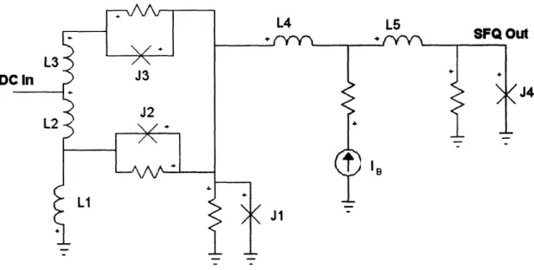
4-4 A design schematic for the DC to SFQ converter. J1-J3, L1-L3 are effectively a hysteretic comparator, while L5, L6, and J4 are an output
4-5 Schematic of SFQ/DC converter. Effectively, we have an input JTL
(J1) which goes to a T Flip Flop (J2-J7). In the 1 state, the output
exceeds the critical current of J9, which produces a series of SFQ pulses at the output. This yields a small DC voltage when low-passed. . . . 53
4-6 Block diagram for the 'Brahman' experiment. This is the most basic
RSFQ circuit that we will design. We will utilize this circuit as a
base-line and testbench for manipulating bias and environment parameters. 54 4-7 Block diagram for the 'Brangus' experiment. This circuit implements
a memory element, the D flip flop. We will utilize this circuit to test the memory lifetime capabilities of RSFQ circuits. . . . . 55
4-8 Block diagram for the 'Hereford' experiment. This circuit implements our SQUID comparator at the input. We will utilize this circuit along
with some standalone SQUIDS to characterize this input stage. . . . 55
4-9 Block diagram for the 'Texas Longhorn' experiment. This circuit can act as a fully functional readout for a single SNSPD. We will test this circuit first to ensure functionality. Next, if all is functional, this circuit will be interfaced to the SNSPD. . . . . 56
5-1 Simulink model for a Josephson junction. We use the RSJ
approxi-mation and include the presence of an external shunt resistance in the
model. Each of our junctions is shunted with approximately 1Q. . . . 58
5-2 Simulink construction of a DC/SFQ converter. We will perform most
of our digital simulation in WRSpice, as it uses more accurate models and is designed for layout. However, our RSJ model suffices to describe basic RSFQ circuits. . . . . 59 5-3 Simulation results for the DC/SFQ converter. This Matlab simulation
accurately reflects the results given in WRSpice, demonstrating the robustness and capability of our model. . . . . 60
5-4 Simulink model of the complete SNSPD and input stage to RSFQ. Note that we have included the newly designed bias tee as the splitter. Finally, the input stage consists of the magnetically coupled SQUID
that we read out. ... ... 61
5-5 Top: detector current; Middle: SQUID output voltage; Bottom:
De-tector Resistance. Note that as the deDe-tector fires, we observe multiple
SFQ pulses being produced by the SQUID comparator. This occurs
because we have biased the SQUID very close to its critical current, so we exceed the critical current by a larger amount, creating a rapid train of SFQ pulses. . . . . 62 5-6 Simulation results for the 'Brahman' test circuit. If this circuit
func-tions properly, an input current square wave will result in SFQ pulses causing the DC/SFQ converter to produce a DC output. Note that because the DC/SFQ converter is effectively a T flip flop, the output frequency will be 1/2 of the input frequency. . . . . 64
5-7 Simulation results for the 'Brangus' test circuit. The top four traces
reflect the input signals and their respective SFQ pulse trains. 'D SFQ' goes to the D port of the flip flop, and when the next clock pulse arrives, we observe an SFQ pulse at the flip flop output. This then toggles the
SFQ/DC converter. . . . . 65 5-8 Simulation results for the 'Hereford' test circuit. Note that we have
tried to mimic the detector current input by having a 20pA peak pulse input with decay time on the order of iOnS. This current profile roughly matches that of the detector. We observe the predicted pulse train from the SQUID, and these toggle the SFQ/DC converter. . . . . 66 5-9 Simulation results for the 'Texas Longhorn' test circuit. The top four
traces are input stage signals and their respective SFQ pulses incident on the flip flop. Flip flop and SFQ/DC output pulses are given. Note that the D flip flop gates multiple pulses from the SQUID comparator
6-1 Simulink setup for the parallel nanowire simulation. Individual detec-tor currents and resistances are shown in dashed/solid, respectively. Note that each 4-port box contains a full thermoelectric model for the
SNSPD. We also tie an inductor to ground in series with the detector.
This is a deliberately fabricated part that aims to maintain constant current in the detectors. . . . . 71
6-2 Results for the parallel nanowire simulation at 9pA total bias. Note that the system oscillates due to the fact that one detector does not fire immediately after another. This results in a type of 'flux trapping' which causes the second detector to switch at a later time, causing
oscillations. . . . . 72
6-3 Simulation results for a properly functioning detector cascade.
Indi-vidual detector currents and resistances are shown in dashed/solid, respectively. Conditions are the same as the oscillating case except bias current has been increased to 10pA. Note that after the switching
event, the current does not redistribute between the two detectors evenly. 74
7-1 Standard design flow for integrated circuit fabrication. This flow is mimicked exactly by WRSpice, which provides integrated software for
each of these steps. ... ... 76
7-2 A schematic of the Hypres stack with each layer designated.[331 . . . 77
7-3 Schematic of how a large series inductance leads to flux trapping. Note that the persistant current will have current such that LI = <Do. Since we have a large inductance, I can be small enough not to exceed Ic of the Josephson junctions. Avoiding large series inductances prevents this problem . . . . . 78
7-4 Schematic of the anodization stack[9]. This corresponds to the Hypres stack as follows: upper and lower Nb contacts are M2 and M1 respec-tively. Junction area is defined by I1A or IC depending on the process
(1kA/cm 2/4.5kA/cm 2 respectively). The insulator is patterned with I1B. Finally, the anodization area is patterned by its own layer, 'A'. . 79 7-5 Example of the abstraction breakage between the DC/SFQ converter
cell and its containing cell. (a) is a figure of the DC/SFQ converter,
(b) is the containing cell, and (c) is a figure of both cells flattened.
Note that certain layers overlap from the outer layer to the DC/SFQ such that the layers have to 'interlock'. This is not desirable because if this dependence changes, it requires the designer to change all of the containing cells at each DC/SFQ instance. . . . . 81
8-1 Measurement of S21 of the probe. This transmission coefficient
indi-cates loss in our system. This measurement is over twice the length of the probe, and as such indicates twice the loss that we will observe from a signal transmitting from the probe head to the instrumentation outside the cryostat. . . . . 86
A-i A schematic of the Hypres stack with each layer designated.[33] . . . 96
A-2 Simulink model of a SNSPD. Note that the electrical model is simply a
constant kinetic inductanc with a series resistance. The thermal model controls the value of this resistor in time by measuring detector current and whether or not a photon is incident. . . . . 100 A-3 Example circuit for simulating a single SNSPD with readout circuitry.
Note that the readout amplifier is simulated as a single 50Q resistor. . 101
A-4 Simulation results from the Simulink thermoelectric model. Note that the simulation properly reproduces previous simulation results for re-sistance versus time and output voltage versus time. . . . . 102
A-5 Model of the probe head. There are three primary flanges connected by posts. Flange 'A' connects the probe head to the 0.5"O.D. tube.
Flange 'B' is the mount for the PCB adapters and shielding can. Flange
'C' is the mount for the incoming fiber line. . . . . 106 A-6 Schematics of the boards for the adapter stack. (a) RSFQ Sample
mount (b) RSFQ adapter board (c) Base board (d) SNSPD mount
List of Tables
4.1 Values of electrical components for the D flip flop . . . . 50 4.2 Values for electrical components in the DC/SFQ converter. . . . . 52 4.3 Values for electrical components in the SFQ/DC converter. . . . . 54
Chapter 1
Introduction
Photon detection is an integral part of experimental physics, high-speed communi-cation, as well as many other high-tech disciplines. In the realm of communicommuni-cation, unmanned spacecraft are travelling extreme distances, and ground stations need more and more sensitive and selective detectors to maintain a reasonable data rate.[10] In the realm of computing, some of the most promising new forms of quantum comput-ing require consistent and efficient optical detection of scomput-ingle entangled photons.[27] Due to projects like these, demands are increasing for ever more efficient detectors with higher count rates.
The Superconducting Nanowire Single-Photon Detector (SNSPD) is one of the most promising new technologies in this field, being capable of counting photons as faster than 100MHz and with efficiencies around 50%.[22] Currently, the leading competition is from the geiger-mode avalanche photodiode, which is capable of
-20-70% efficiency at a -5MHz count rate depending on photon energy.[18]
In spite of these advantages, the SNSPD is still a brand-new technology and as a result they do not have the same support hardware support as other detectors. As such, SNSPD's are much more difficult to integrate into an existing an experiment. Because of this difficulty, SNSPD's have not been deployed extensively for research or industrial applications. The signal analysis chain that is connected to this detector is one of the key choke points.
frequency on the order of 100MHz. Currently, this signal is processed outside of the cryostat with a series of RF amplifiers and a high-speed counter. This design works for detector prototyping, but poses a series of problems with actual design implemen-tation. Most importantly, it prevents our design from being scalable. Even though we can fabricate thousands of detectors on a single wafer, it would be extremely difficult to place that many RF lines without crosstalk or other interference.
The purpose of this thesis is to build a more robust and scalable readout tech-nology for SNSPDs. First, we will develop intermediate technologies that improve upon current readout technology and will be necessary to develop the final goal. Ul-timately, we plan to build circuitry on-chip that will first convert each detector's analog signal to a digital signal and then condense the data from each detector into an externally clocked, single-bit output indicating the presence or absence of a photon at any detector. This will allow simultaneous readout of a large number of detectors on a single wafer. Additionally, our cryogenic will decrease the noise observed by the detector, as the amplifier is no longer operating at room temperature. Finally, our readout will provide a simple hardware API to be interfaced to a computer or embedded processing unit.
The catch to this development process is that the entire system must operate at 4.2K or below. As such, one must either use HEMT CMOS or Rapid Single-Flux-Quantum (RSFQ) logic. HEMT CMOS is better suited to analog amplification of the output signal, while RSFQ circuitry is better suited to the construction of the
SNSPD interface and digitial logic.
RSFQ circuitry is better suited as an input stage because input amplification with CMOS is difficult, as one must operate in the linear regime of a HEMT. This requires
on the order of 1 mA at 1.8 V minimum, which results in approximately 2 mW per stage. This is to be compared against RSFQ comparators which utilize approximately
0.5 mA at almost no voltage, resulting in muW of dissipation per stage. Given that
we are hoping to produce a large number of SNSPD input stages, RSFQ is clearly a better choice. However, we only have a small number of output signals from the cryostat, so it is much more reasonable to use CMOS, as we can attain larger signal
Figure 1-1: An electron micrograph of an example Superconducting Nanowire
Single-Photon Detector (SNSPD). Current flows through the meanders in the middle from
pads on either side. The wires in the meander are approximately 100 nm wide. Note
that the additional formations exist to balance the dose between the edges and the
middle of the detector.
amplitudes.
1.1
SNSPD Physics
This photon detector consists of a meandering superconducting nanowire biased close
to its critical current. In this regime, a single incident photon can cause a section
of the detector to switch to normal conduction, producing a voltage pulse due to its
now-finite resistance. An electron micrograph is given in figure 1-1.
1.1.1
Hotspot Theory
When a section of the detector goes normal due to an incoming photon, the effective
resistance of the detector increases dramatically, and therefore the current though the
detector drops temporarily.
Now, two things happen simultaneously. First, the heat localized in the hotspot
must diffuse to other parts of the detector or substrate. Second, the detector is
inductive, so there is an L/R relaxation time of current returning to the detector.
However, these are competing processes. Any current through the detector will
Figure 1-2: This is a schematic of how an incident photon produces a voltage pulse
at the output. At (a), an incident photon is absorbed to produce an initial hot-spot
shown in (b). The diverted supercurrent exceeds the critical current in the
now-constricted wire in (c). Finally, a small section of the wire becomes fully resistive in
(d), producing a voltage pulse.[23]
end up in joule heating of the resistive section of the detector, extending the amount
of time it takes to cool the hotspot back down. There are two stable states to this
system. The system can either relax to the superconducting state, or it can 'latch'
into the normal state. When a photon is incident on the detector, the L/R reset time
determines which of these states the system resets to. Generally, longer L/R time
constants result in resetting to the superconducting state, while shorter L/R results
in latching.[32][15]
These two time constants determine the output pulse size and therefore the
max-imum count rate of the detector.
1.2
Current Readout Status
Currently, all SNSPD readout techonology takes place outside of the cryostat. A
schematic of the RF setup required is shown in figure 1-3. This system is not scalable
to multiple SNSPDs, as each SNSPD would require an individual bias line, which is
not feasible.
Bias Tee Low-Noise Current
0.1 MHz Cutoff Supply P-10%uA)
To Detector
dB Attenuator In
Out 3x 10dB Arnplifier G!0XIMHz) LeCroy E2X]A Waverunner
Oscilloscope (50 Ohms)
Figure 1-3: Schematic of current RF/DC setup. Each of these electronic components lies outside of the cryostat. As a result, the system must be very well shielded and
50Q matched to prevent noise from overcoming our signal.
1.3
Project Scope
The goal of this project is to develop a fully integrated readout system. A schematic is given in 1-4. We will be replacing all of the RF circuitry discussed in the previous section, and replacing this with processing technology that exists on-chip.
This project consists of several facets which will ultimately come together for a full readout. First, we have the RSFQ circuitry which will serve as the dominmant amplification and processing technology. However, we will also design some analog interfaces which will enable RSFQ to be used. In addition, I will quickly discuss some adaptations of the detector itself which can make readout easier.
1.3.1
Rapid Single-Flux-Quantum (RSFQ) On-chip Readout
RSFQ circuitry will provide most of the functionality as an on-chip readout. This
circuitry is comprised of an input SQUID comparator, basic digital processing, and
DC/SFQ converter units. Our initial circuit design is very simple, as we wish to
characterize the fabrication process, our experimental setup, and SNSPD/RSFQ in-teractions. However, in principle, this digital design is highly scalable, allowing for complex digital analysis of incoming SNSPD signals.
Detectors Pulse Out Input Bulfer Inside Dewar Outside Dewar
I
or -
4.2K
298K
-+ ...>1 or 0
Computer Interface
Scope of this Project
Figure 1-4: Schematic of the scope of this project. Digital logic is constructed utilizing
RSFQ technology. Additional (unshown) analog interface circuits will be discussed.
1.3.2
Cryogenic RF Electronics
In order to use RSFQ circuitry, we must first adapt the detector output to prop-erly channel its signal into the RSFQ comparator. This cryogenic bias tee has been designed and fabricated. In addition, we must provide a proper interface between the RSFQ outputs and traditional CMOS logic. Since RSFQ utilizes much smaller signal amplitudes than traditional CMOS, it will be necessary to design a cryogenic amplifier to boost these signals.
1.3.3
Detectors in Parallel
We will quickly discuss one way to modify the detector itself to aid in the readout process. If one utilizes multiple SNSPDs in parallel, the signals from each photon detected causes an avalanche which is substantially easier to read out.
However, this topology is significantly more complicated than a single nanowire,
and therefore contains complex dynamics. Analysis and models constructed for
SNSPD/RSFQ interaction analysis are also used to better understand these dynamics
and their effect how we read out these parallel detectors.
Chapter 2
Cryogenic Amplifier
For our scalable cryogenic readout, we require an RSFQ input stage which converts each detector pulse to a digital SFQ signal. However, we ultimately must convert this signal to a DC voltage to be read by traditional room-temperature CMOS logic. This is difficult, as RSFQ circuits can only output fractions of a mV. Therefore, we need additional amplification on the back-end.[31]
Although we could not use a cryogenic amplifier for each of the detectors due to power considerations, there are far fewer output signals from the RSFQ circuitry that must be amplified. Therefore, we can now use a cryoCMOS amplifier without fear of dissipating too much energy inside of the cryostat. In addition, the bandwidth of this detector is broad enough to amplify single detector pulses as well. Although it is still difficult to read out multiple detectors, there are a number of advantages to amplifying the detector signal close to the detector: we decrease noise seen by the detector, which increases our SNR of the pulses coming out of the cryostat.
2.1
Cryogenic Electronics Considerations
Most electrical devices are rated for around 300±40K. This rating is mostly package-driven for high-temperatures. For cryogenic considerations, there are a different set of considerations that must be taken into account. These problems vary depending on the component in question.
First, many resistors are highly temperature dependant. High-value carbon re-sistors use stacked Metal-Insulator-Metal tunnelling junctions to achieve this high resistance. However, the behavior of this physical phenomena changes dramatically at low temperatures. [16] Therefore, one must use lower-value metal film resistors which have much better behavior at low T. These resistors depend only on the re-sistivity of a given metal and therefore behave well at low temperature. The most common materials for thin film resistors are NiCr, TaN, and PbO. None of these be-come superconducting at 4.2K. Given a linear 25-50ppm/oC temperature dependence (as specified in the data sheet), we can expect between 10-15% value change maxi-mum between room temperature and cryogenic temperatures. This extrapolation is supported by experimental findings[24]. This change in resistivity is acceptable for our purposes, as our resistor values are not tightly specified.
Next, electrolytic capacitors require mobile ions in a solvent in the capacitor itself to achieve its rating. However, once the solvent freezes, the capactor value drops dramatically. Therefore, it is only prudent to use chip capacitors with solid dielectrics. In this case, the dielectric constant is much less sensitive to temperature change and does not 'freeze out' like electrolytic dielectrics. The best options are polymer and low-K ceramic capacitors. High-K ceramics tend to use complicated materials as dielectric. The physics of these materials is not guaranteed to function at low temperatures. [16]
Finally, MOSFET's and BJT's also do not function at low temperatures. Basic semiconductor technology utilizes doping to provide free carriers. However, these dopants have a specific ionization energy (which is usually less than KT). However, as one cools the transistor, the number of free carriers drops dramatically as the dopant sites retrap their carriers. HEMT and p-HEMT transistors address this problem by using a heterojunction which uses differences in bandgap to displace carriers away from the doped material.[8] Specifically, one uses N doped AlGaAs (relatively large bandgap material) sandwiching a thin layer of InGaAs (lower bandgap materal with a lower energy conduction band).
N Dopant
Sites
EF E.t
Upper Chamel Lower
Barrier (InGaAs) Barrier
(AlGaAs) (A1GaAs)
Figure 2-1: Schematic of a HEMT band diagram. Note that the carrier channel is dis-placed from the doping sites, thereby preventing retrapping at low temperatures. [3].
Now, with an applied voltage at the gate, we can decrease the energy of this conduc-tion band below the Fermi energy of the contacts, and conducconduc-tion is allowed. This interests us, however, because the carriers are now displaced from the dopant sites, so there is no retrapping. Therefore, freeze-out cannot occur, and these devices behave well even at cryogenic temperatures.
2.2
Amplifier Topology
Despite the difference in microphysics, a HEMT has the same basic behavioral char-acteristics as a standard MOSFET. Therefore, we can use the standard topologies for amplification that have been developed for MOSFET technology.
Our first amplifier design used a common-source topology. This topology allowed us to derive the most gain from our devices, but also had the side-effect of having a high input impedance to the transistor (a small capacitive load, Cg,). A high impedence input is traditionally desirable, but it can potentially become a liability at UHF frequencies, as it may cause a 50 Q matched system to become unstable.
At this point, it must be mentioned that we are mounting our amplifier geomet-rically close to the detector, and as such the amplifier will not see 50 Q at its input. Rather, we can treat the SNSPD as a freewheeling inductor. However, if we stabilize
'mNNWsF 100000pF 00=1M LI % D001mm 1000pF -_ vv v C2 VA2.Gn" R1 01a C1 PNUh2 POn2
PNw
W
RZ1=1.6mmFigure 2-2: Schematic of the cryogenic amplifier design. The active element is an Avago ATF-55143 enhancement pHEMT.
our system properly, we should not observe oscillations in either of these cases. Note also that in our single-stage implementation above, we do not match the output to 50 Q either. We have made this choice because we need more gain than is available if we match the output to 50 Q. The impedance mismatch is not a huge problem for us, as we are not terribly concerned about reflections off of this node, but should it become an issue, it is easily resolved by either using multiple stages or using a source-follower impedence matching circuit. Such an addition will not remove bandwidth from the system. The only downside will be increased power draw.
Traditionally when designing RF circuits, one aims for a specific (narrow band) region of amplification. We are looking for much more broadband amplification, so
I used a different strategy than most RF amplifiers. We are operating at such a
low frequency (0.01-2GHz), that instead of utilizing the HEMT S-Parameters, we can roughly approximate our HEMT (Q1) as having infinite input impedance in this region of input frequency with a small capacitance from gate to source. In order to maintain a relatively constant input impedance, I added a small inductance (LI) to the input termination to compensate. However, the most important element is the gate resistor (1). This resistor decreased the transconductance of the stage as less voltage was seen between the gate and source of the HEMT at high frequencies. This reduction in input signal was necessary, as the HEMT had significant transconduc-tance even at very high frequencies. If we had not compensated for this, the system would have become unstable at high frequencies (1-2GHz). We could see this by ob-serving the K stability factor. If this factor is less than 1, our system is conditionally stable: [2]
1 - |S11 2 __ I2212 + A12 (2.1)
K =-21
21S12S211
where A = S11S22 - S12S21. This factor becomes small when
IS
1 2S2 11 becomesof order unity. At low frequencies, the reverse transmission S12 is very low, so the system is stable. However, past 1GHz, S12 begins to approach unity. In order to keep
However, we have chosen to not match our system perfectly to achieve better gain characteristics. Therefore, we decrease S2 1 at high frequencies with the gate resistor
Ri.
The downside to this approach is that it increases our noise substantially since Johnson-Nyquist noise is directly amplified by the high-impedance node of the com-mon source amplifier. Therefore, we make RI as small as possible without destabi-lizing the circuit.
2.3
Simulations
After simulating this circuit, there are several interesting features to note. However, we must keep in mind the limitations of our simulation. First, we have simulated our system with a 50 Q source and load. While the latter is accurate, our detector is far from 50 Q. In reality, it can be only really be understood as a constant inductance with some varying resistance in time (corresponding to an incident photon and heat dissipation). This system is highly nonlinear and as such cannot be simulated as a small signal model. We have addressed this problem by building an appropriate detector model in Simulink, and then reconstructing the input stage of our amplifier as a load for the photon detector and performing a transient simulation. These simulations have shown that the input stage does not oscillate, so the impedance mismatch does not create problems.
Simultaneously, if this amplifier will be used for RSFQ circuitry it will see a low impedance output from the RSFQ circuitry. The SFQ to DC converter has an output impedance equal to the normal resistance of the Josephson junction in parallel with its shunt resistor. The shunt resistor is much smaller than the Junction resistance at 1 Q, so the amplifier will see a 1 Q voltage source. This also is not problematic, because in both of these cases the amplifier will be exceedingly close to the operating device with respect to the wavelength of the incoming signal. Therefore, we do not need to view the input as coming from a transmission line.
00---40
--60
10 10 102 10 10* 10
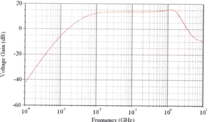
Frequency (GHz)
Figure 2-3: Figure of gain versus frequency. Note that there is a small amount of peaking around 2GHz. This is due to the small value of the gate resistor.
parameters, so we will assume a 50 Q input and keep in mind that this impedance is not the impedance of the detector. Therefore, the simulation is not numerically accurate, but provides insight as to the behavior and stability of the amplifier.
A second shortcoming is that we must simulate at room temperature (300K). This
is due to the fact that there is very little real data as to the temperature dependance of passive parts on that extreme of a temperature range. As a result, dramatically changing the temperature in simulation does not accurately reflect device perfor-mance. However, we have taken proper precautions to use passive parts that will not deviate from their nominal values much at cryogenic temperatures. The HEMT may potentially cause instability at low temperatures, as its gain increases slightly as temperature decreases. This problem will be discussed further later.
The maximum available gain of the device (calculated from S parameters on datasheet) is approximately 15dB over the range of interest. We have achieved slightly less than 15dB gain between 20MHz and 2GHz. (See figure 2-3)
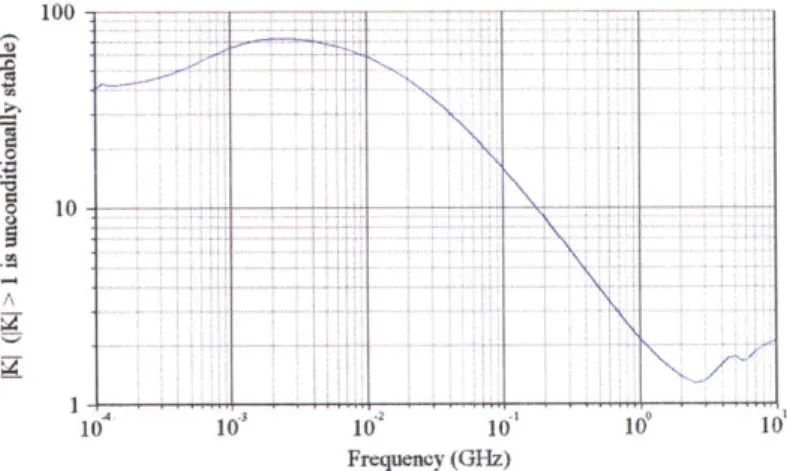
Note that our stability factor (K) becomes very close to 1 (below 1 indicates insta-bility) slightly above 1GHz. This dip in the stability factor is due to the inductively coupled terminations having a slightly underdamped resonant system with Cgs of the transistor. This behavior of this resonance also explains why we stabilize our system when we increase the resistance of the gate resistor. This resistor is effectively a
100 -0 10 W* 16 1 101 010 10" 10' Frequency (GHz)
Instead of utilizing the HEMT S-Parameters,
Figure 2-4: Stability factor K of the amplifier for varying frequencies. Note that this is simulated at room temperature for 50Q input and output impedances. Therefore, we can assume a reasonable amount of error associated with this simulation.
damping resistor. However, we have minimized this value to achieve minimal noise figure, therefore our system is slightly underdamped, leading to some peaking in the gain curve and resultant decrease in the stability of the circuit. This peaking behavior is worsened by the fact that our HEMT has increased gain at low temperatures.
However, there is one additional unsimulated factor that will prevent our system from oscillating. We are building our circuit on an FR4 substrate. FR4 is the standard PCB material and behaves well below 1-2GHz. At and above these values, FR4 be-comes lossy. Therefore, we will not observe significant gain peaking in this frequency range, as our substrate will be the ultimate limiting factor. If it becomes necessary to understand this loss further, one can gain additional understanding of this loss through lossy transmission line theory with transmission line capacitor shunted by a resistor simulating the loss.
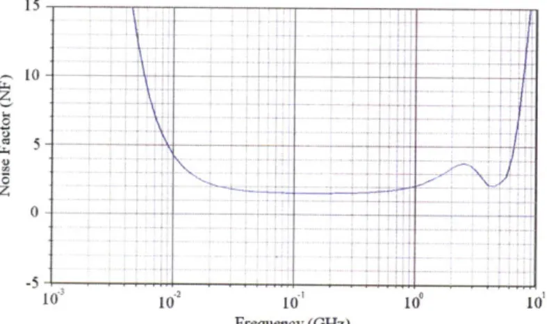
Our noise figure simulation is probably the least accurate of the simulation data we have collected for two reasons: (1) we simulated at room temperature, so all of our resistors are contributing full 300K Johnson noise; and (2) the HEMT noise figure is not well defined over the frequencies of interest, but is claimed to be approximately between 0.3-0.6dB at room temperature and decrease as temperature decreases. In summary, the simulated values are an overestimate of noise figure.
-54 4 44
10 10 10 10* 10
Frequency (GHz)
Figure 2-5: Noise factor of our amplifier. Note that this is an overestimate because we have simulated our amplifier at 300K, so the Johnson noise of our resistors will be much larger than at 4.2K where the amplifier will operate.
to-2 0-1 10 10 Frequency (GHz) Si S21 S22 S12 -Figure 2-6: larger than application
S parameters for the cryogenic amplifier. Note that S11 and S22 are
is usually acceptable. This mismatch is a design choice specific to our which enables us to get additional gain.
15 10 -5 -10 -15 - - - -V 0.1 0.2 0.5 1.0 2.0 5.0 10.0 Frequency (GHz)
Figure 2-7: Measured S21 parameter at room temperature. These results follow exactly what we expect. Note that we have a slightly decreased bandwith and no peaking between 1 and 2 GHz due to the loss in the FR4. The additional peaking above 5GHz is disconcerting, but will not be observed, as the loss in the probe is much greater than 5dB at 5GHz.
Finally, we have simulated scattering parameters for the amplifier. This plot is revealing as to the limitations of this amplifier. Since we have not matched input or output very well to 50 Q, our S11 and S22 parameters are relatively large. However, I argue that this is acceptable for our applications. Our input will not be 50 Q matched, and some reflections off the output are acceptable as the other end of our system will be properly terminated.
2.4
Results
We constructed an amplifier and it worked as designed. We first characterized gain as a function of frequency directly, as shown in figure 2-7. Note that we observed a roll-off in gain at about 1-2GHz as expected, but we did not observe any gain peaking or indications of instability at this frequency. On the other hand, we observed a gain peak between 5 and 10GHz. This peaking is most likely due to self-resonance of the passive components (the inductor (L1) in particular). While this is bothersome, it turned out to have little importance due to additional losses from the cryogenic probe
on which the amplifier is mounted.
-10
-20 --
t
-30 __
0.1 0.5 1 2
Frequency (GHz)
Figure 2-8: Measured S21 of the amplifier when attached to the probe. Note that now we have less gain and a very sharp cutoff just below 800MHz. This is due to the loss of the probe.
We have also characterized the transfer function of the amplifier when mounted on the cryogenic probe. This curve is shown in figure 2-8. Note that we observed a dramatic cutoff in gain at 800MHz. This was due to the fact that the probe head had significant parasitic capacitance. As a result, high frequency signals were lost. This capacitance removed the peaking behavior of the amplifier but also limits our bandwidth.
In the above plots, note that we have characterized the S parameters from 50MHz to 2GHz due to the lower frequency limit on our network analyzer. Below this fre-quency we used a spectrum analyzer to verify the s2 roll-off at 20MHz (not shown).
However, the higher frequency characteristics are more critical to our application, therefore we focus our analysis here.
2.5
Possible Improvements
This first cryogenic amplifier is a single-stage common source amplifier. There are several simple methods of improving this topology should additional specifications need to be met. For example, if the gain is not high enough or we need to match output impedance, we can add an additional source follower onto the output of the
common source amplifier. This will provide a low-impedance output which we can match to 50Q. In addition, the intermediate impedance between the common source amplifier and source follower can take any reasonably low value, so we can choose to have a larger amount of amplification than is possible with a single stage.
R4 R R9 R10 RF+DC 1.5k 1.8k 1.5k 5k RI LI L2 L3 14 DC 50 330n 'R5 910n lR618p R7470p R11 0.05p .5k 1.5k 5010k
1c2
C3
C4
R3 RF P iop 0nFigure 2-9: Reverse-engineered schematic of the currently used bias tee (Mini-Circuits ZFBT-4R2G+).[1] This tee is 50Q matched at all inputs. The analog in-ductor/capacitor values are far too large to fabricate on-chip.
2.6
Cryogenic Bias Tee
One of the most crucial technologies enabling our single photon detector is the bias tee, which allows a DC bias current and RF signal pulse to travel along a single RF-coax line and subsequently be separated. Typically, a bias tee is implemented in figure 2-9.[12]
Note that this is basically just an LC circuit with stacked inductors to successively remove incrementally lower frequencies. The use of incremental stages is necessary because the larger inductors have self-resonances at frequencies of interest. Also, the entire system is 50 Q matched on the RF-DC and RF ports.
Ultimately, we are trying to achieve scalability of design. We need to bias and read-out multiple detectors on a single chip. The problem then arises that the our detectors are of the order 10-100pm2, the RSFQ circuitry for each element is on the
same order of area, but the bias tee connecting them must be large due to its large passive elements. Therefore, we must find a technology that has the same order space requirements as the detector/RSFQ circuitry.
The solution lies in the fact that our system is not 50 Q matched, and our cutoff frequency can be much higher than standard bias tees (most of our frequency com-ponents lie between 1MHz and 1GHz). Taking this into consideration, we consider the passive elements available to us with each of our fabrication processes. With Hypres's tri-layer Nb process for RSFQ circuits and the current space requirements,
RF Out
Detector Model
100n 1RM
Figure 2-10: Schematic of the new bias tee design. Note that it consists only of an on-chip inductor utilizing kinetic inductance to achieve the large value. Note that we include a 50 Q termination on the current source to simulate a low-impedance cable.
we can fabricate capacitors with values on the order of 1pF or below, inductors with values on the order of 100's of pH or below, and resistors with values on the order of
100 Q or below.[20] None of these values is large enough to create a cutoff below our
required frequency of 1-10MHz.
Next, if we consider the process we use to actually fabricate detectors, we observe that we cannot fabricate resistors. We cannot fabricate capacitors with significant values. However, due to the fact that the film is 4nm, we measure a kinetic inductance of approximately 80pH/sq. This allows us to construct 400nH inductors with an area comparable to the size of the detector. Now, this will be an on-chip construction, so consider the circuit in figure 2-10.
Note that this works properly as a bias tee. Since the SNSPD has no resistance to ground, the DC current will pass entirely through the SNSPD. Also note that AC signals above the first order cutoff of L/R will pass through the amplifier. This roll-off frequency can be calculated to be 20MHz.
There are several important notes to this implementation. First, since we have no capacitance in this system, we have only a first order roll-off, so the cutoff is not precise. In reality, we have nonideal behavior below 200MHz.
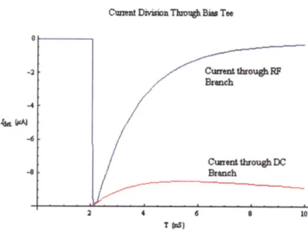
Probably the most important to note is how we view the current source.
Cumnnt Divisn Throgh Biu Tee
2 4 6 0 10
T inS)
Figure 2-11: Results for simulations of the bias tee with a SNSPD detector pulse. The blue line shows the current through the 50 Q amplifier, and the red line shows the current lost into the current source. The original signal amplitude is 10pA. ally, this current source would be high impedance, but since we are looking at UHF frequencies and the current source is removed from the system, we cannot use this approximation. Instead, we must recognize that our probe station (where we test this circuit) utilizes a 50 Q probe to apply the DC bias current. Therefore, at the frequen-cies of interest, we will see the impedance of the cable. In addition, to practically prevent coupling too much electromagnetic noise to the system one must terminate the current source with 50 Q, so the above model is accurate.
This implementation immediately lends itself to multiple potential improvements. First, in the final implementation, we do not need a 50 Q RF coaxial line to bias the detector at DC. In reality, we only need an unshielded bias line with a ferrite bead RF choke near the detector. The RF choke will dramatically increase source resistance and decrease our cutoff frequency. This improvement is a part of the final experimental setup.
Chapter 3
RSFQ Theory
Rapid Single Flux Quantum (RSFQ) logic uses Josephson junctions as the switching element much like CMOS logic uses MOSFETS as the switching element. However, beyond having active elements, RSFQ and CMOS logic are dramatically different.
RSFQ circuitry is faster and uses less energy than traditional CMOS logic. This
logic has been used to create frequency downconverters that operate up to 750GHz.[6]
Also, basic 4/8 bit processors have been implemented that operate at frequencies of 10s of GHz.[4] However, given the cryogenic and shielding requirements for such circuitry to operate, RSFQ has never become mainstream, remaining a niche tech-nology for specific applications. In addition, silicon CMOS techtech-nology has advanced so quickly that most speed advantages of using RSFQ have been marginalized. Cur-rently, RSFQ only offers a factor of 3-5 speedup over mainstream CMOS technology. Therefore, it is extremely unlikely that RSFQ will ever compete with CMOS for main-stream usage. However, as it turns out, RSFQ is very well suited for developing a cryogenic readout for SNSPDs. RSFQ lends itself to this application for two primary reasons. First, our system is already cryogenic, so standard CMOS technology is not an option. Second, we can only sustain a minimial heat load, so the energy advantage of RSFQ logic makes it an excellent engineering choice.
To understand how RSFQ circuitry works, one must first understand the basics of how the Josephson junction works.
3.1
Josephson Junction Physics
This fundamental superconducting element is typically comprised of a superconductor-insulator-superconductor (S-I-S) stack where the insulator is extremely thin and al-lows quantum tunneling of Cooper pairs through the barrier. In reality, this can be any form of weak link, but we will be using oxide tunnelling to achieve this effect. Possibly the least intuitive process of Josephson junction physics is that Cooper pairs do not break before tunneling. Instead, the macroscopic phase parameter is corre-lated from one side of the junction to the other just as if the entire superconducting wavefunction were treated as the tunneling particle, rather than the individual
wave-functions for each electron. [21] [28]
The superconducting wavefunction can be approximated as:
1
ql(S) = e (3.1)
where n* is the density of superconducting charge carriers, and 0(i) is the local phase of the wavefunction. Now, utilizing Ginzburg-Landau theory, we can derive the current of the macroscopic quantum wavefunction to be:
Js = 2q*Re
V
(3.2)
where m* and q* are the effective mass and charge of the carriers. For the case of a Cooper pair, m* = 2me and q* = 2q,. Now, if we derive the wavefunction across a
barrier, we can observe the current across a junction. Consider a potential show in figure 3-1.
Now, let us consider the solution in all three sections of the potential. The solution on either side of the barrier is simply the solution given in equation 3.1.
In the barrier however, the solution becomes exponentially decaying in x:
Alf(x)
=
C1 cosh - +
C
2sinh -
(3.3)
Superconducting Insulator Superconductmg Contact I Contact 2 V(x) Josepson potetid V, Superconducting Wavefkictiofl Enavj, -a +Ia hisulator Boundanies
Figure 3-1: Basic Josephson junction potential. Energy of the superconducting wave-function is given as E0, which is less than the barrier height. Image courtesy of
[21]
phases 01 and 02 on the left and right hand side of the potential, respectively. Now, we match boundary conditions and derive C1 and C2.
C1= Vnel
+
rieiO2 (3.4)2 cosh(a/()
C2 = 4eio1 - nei02 (3.5)
2 sinh(a/()
Finally, we use our equation for J, and derive the DC Josephson effect:
J, = Je sin(01 - 02) (3.6)
where the Josephson critical current density Jc = mn( sinh(2a/C) 'mes/c). In real applications,
we do not have exact control over the potential barrier, we generally consider Je to be a fundamental parameter of a specific process, rather than a derived property as it is shown above.
Now, to consider a voltage across a junction, let us work backward from the answer. We will derive that a voltage creates a linear increase in phase in time, so let us consider the rate of change of the gauge-invariant phase across the Josephson junction. Let 8(t) be this gauge-invariant phase difference. We must subtract off a
line integral of the magnetic field to maintain gauge invariance.
ae
80a
1 0022ir
8
2_-8- =~
--
- -- -2-
2
B (F)t) -dl
(3.7)
at
at
at 4)0 t
1,
where the integral is a path integral of the vector potential from one node of the Josephson junction to the other. Now, we note the supercurrent equation at the boundaries:
-6(Ft) = - "(A +q*#O (it) (3.8)
Sth
2n*
We plug this in and cancel terms to show that:
68 2 2 - 27
-
-
-
(V - V)
(3.9)
Rt
Qo
16t)
Q o
Note that the above integral is an integral of the gauge invariant electric field across the Josephson junction which yields the voltage across the junction. Therefore, we have related the voltage across the Josephson junction to the time rate of change of the phase across the same junction.
In conclusion, we have derived constitutive relations for the Josephson junction:
I(t) =
Ic
sin(E(t)) (3.10)V (t) =D
8
E(t)
(3.11)
2w 6t
where 8(t) is the phase across the Josephson junction. If
e(t)
is constant in time
and arbitrary in value, this means that the current can take any value between 0 and
Ic
without developing any voltage across the Josephson junction. Note that these equations are highly nonlinear and not linearizable for any nonzero voltage. This is the source of the difficulty with analyzing Josephson junction circuits. This difficulty will become apparent when we try to establish a rigorous design methodology for digital circuits using this technology.tot
Ir
I
SI,
Figure 3-2: Schematic of RSJ model. Note that the element in the middle is the ideal Josephson junction with relations given by 3.10 and 3.11. The R and C elements represent unavoidable aspects of the Josephson junction.
3.2
Resistively Shunted Junction Model
The Resistively Shunted Junction (RSJ) model attempts to model the nonideal ele-ments of Josephson junctions by using a shunt capacitor and resistor. The capacitor takes into account the capacitive effect that occurs with two parallel plates of su-perconductor with an oxide layer between. The resistive shunt tries to approximate the single-electron tunneling through the oxide barrier. The capacitive approxima-tion is very accurate, as a juncapproxima-tion really is just a parallel plate capacitor. However, the resistive approximation fails to approximate the subgap resistance, which will be discussed later.
Note that in the RSJ model, we can break down the overall differential equation governing behavior into the following:
1 GDo a
GDo a2
tot =
Ic
sin(O) + 0 + C 6t (3.12)R 27r
at
2,r 82twhich looks exactly like the differential equation for the full nonlinear dynamics of a pendulum.
F = mgl sin() + b O+ ml2
02 0(3.13)
Note that in this analogy, the capacitance becomes a 'mass' term, resistance be-comes the 'damping' term, and Itot bebe-comes equivalent to a 'torque.' With this analogy, we can understand the dynamics of how a current affects the phase. Now, consider with the pendulum analogy what happens if we have a heavily overdamped system. Mechanically, the damping term corresponds to frictional resistance at the pivot, while for Josephson junctions, it corresponds to a small shunt resistor.
If we give the pendulum a 'torque' that is small enough, the system will reach
some steady state angle
0.
This angle must be less than r/2, as gravity provides the strongest force at this angle. If any more torque is added to this 'critical torque', it will cause the system to oscillate. This 'critical torque' is the same as the critical current of a Josephson junction. A bias current in excess of the critical current will cause the phase of the junction to oscillate in the same way as the pendulum.Now, if we bias the junction close to its critical current, this picture is analogous to providing torque slightly less than that which is required to make a pendulum oscillate. Now, in the mechanical picture, if one gives the pendulum a small kick, the pendulum rotates by 27r and returns to its original position without rotating further (assuming overdamping).
With the Josephson junction, an analogous event occurs. We bias the junction very close to its critical current, apply a small voltage pulse, and observe an output voltage pulse resulting from the phase changing by 27. Note that this pulse has an area of <Do and also corresponds to a single magnetic flux quantum passing through the Josephson junction. These pulses will be the basis of RSFQ logic.[13][17]
One important note that has been alluded to is that the RSJ model is far from perfect. This error manifests itself in the shunt resistance. We are approximating this shunt resistance as a pure ohmic resistor. This models a single-electron tun-nel junction with a constant density of charge carriers, and is far from completely accurate. In reality, with V > 0, there is a strong nonlinear current dependence
below Vg = IcRn, where Rn is the normal (Ohmic) resistance at higher currents. This nonlinear resistance is called the subgap resistance (Rsg), and is usually very large. [17]