Supporting Information for “Polymer Encapsulants
for Threshold Voltage Control in Carbon Nanotube
Transistors”
François Lapointe1 *, Ashish Sapkota1,2, Jianfu Ding1, Jacques Lefebvre1 1. National Research Council Canada
1200 Montreal Road Ottawa, Ontario Canada, K1A 0R6
2. Department of Printed Electronics Engineering Sunchon National University
Sunchon 540-742 Korea * Corresponding Author [email protected]
Table of Contents
Methods - Polymer Encapsulation- Capacitive Probe for Charge Density Measurements - Determination of threshold voltage
Additional Results - Annealing Step - P2VP / PS Blends
- Other Parameters Extracted from P(S-co-2VP) Copolymer Series - General Trends of Threshold Voltage against Various Charge States - Additional Results of the Threshold Voltage against Charge Density at VT
- PVAc Thickness Series
Methods
Polymer Encapsulation
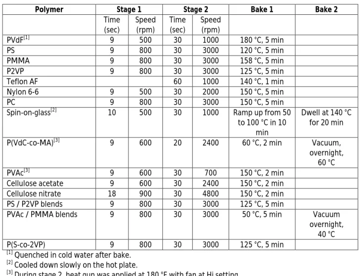
Capping of the CNN-FET dies was achieved according to the procedure described in the “Methods” section of the main text with the conditions detailed in Tables S1 and S2. Some solutions required filtration using 0.45 μm PTFE cartridge syringe filters in order to get a smooth layer. The different bake temperatures were chosen according to the reported glass transition temperatures of the polymers and the boiling point of the solvents or following the instructions of the manufacturer.
Table S1. Conditions for preparation of solution
Polymer Solvent Concentration (% w/V)
Filtered 0.45 μm PTFE?
PVdF DMF 10 No
PS Chloroform 15 Yes
PMMA Chloroform 15 Yes
P2VP Chloroform 15 Yes Teflon AF As is As is No Nylon 6-6 m-Cresol 5 No PC Chloroform 10 No Spin-on-glass As is As is No P(VdC-co-MA) NMP 10 No PVAc DMF 15 No Cellulose acetate DMF 7.5 No
Cellulose nitrate Diethyl ether / ethanol 1 : 2 collodion : ethanol No
PS / P2VP blends Chloroform 15 Yes
PVAc / PMMA blends Chloroform Varying from 15 to 5 No
P(S-co-2VP) copolymers
Table S2. Conditions for spin coating
Polymer Stage 1 Stage 2 Bake 1 Bake 2
Time (sec) Speed (rpm) Time (sec) Speed (rpm) PVdF[1] 9 500 30 1000 180 °C, 5 min PS 9 800 30 3000 120 °C, 5 min PMMA 9 800 30 3000 158 °C, 5 min P2VP 9 800 30 3000 125 °C, 5 min Teflon AF 60 1000 140 °C, 1 min Nylon 6-6 9 500 30 2000 150 °C, 5 min PC 9 800 30 3000 150 °C, 5 min
Spin-on-glass[2] 10 500 30 1000 Ramp up from 50
to 100 °C in 10 min
Dwell at 140 °C for 20 min
P(VdC-co-MA)[3] 9 600 20 2400 60 °C, 2 min Vacuum,
overnight, 60 °C
PVAc[3] 9 600 30 700 150 °C, 2 min
Cellulose acetate 9 600 30 2400 150 °C, 2 min
Cellulose nitrate 18 900 30 4800 150 °C, 2 min
PS / P2VP blends 9 800 30 3000 125 °C, 5 min
PVAc / PMMA blends 9 800 30 3000 50 °C, 5 min Vacuum
overnight, 40 °C
P(S-co-2VP) 9 800 30 3000 125 °C, 5 min
[1]
Quenched in cold water after bake.
[2]
Cooled down slowly on the hot plate.
[3]
During stage 2, heat gun was applied at 180 °F with fan at Hi setting.
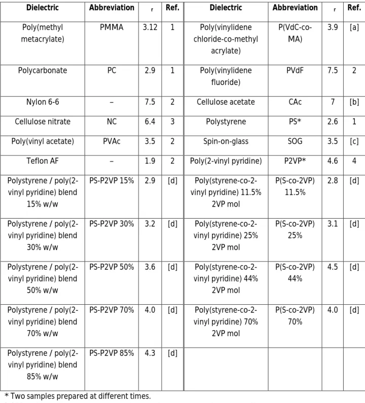
The relative permittivity values of the polymers were found from various sources in the literature. We settled on the use of reported values as it enters only in the calculation of the gate capacitance, where the effective relative permittivity consists of an averaged value with the underlying silicon dioxide. This reduces the impact of the value of the polymer relative permittivity on the final result.
Table S3. List of dielectrics tested for the threshold voltage – charge relationship and their relative permittivity values.
Dielectric Abbreviation εr Ref. Dielectric Abbreviation εr Ref.
Poly(methyl metacrylate) PMMA 3.12 1 Poly(vinylidene chloride-co-methyl acrylate) P(VdC-co-MA) 3.9 [a] Polycarbonate PC 2.9 1 Poly(vinylidene fluoride) PVdF 7.5 2
Nylon 6-6 – 7.5 2 Cellulose acetate CAc 7 [b]
Cellulose nitrate NC 6.4 3 Polystyrene PS* 2.6 1
Poly(vinyl acetate) PVAc 3.5 2 Spin-on-glass SOG 3.5 [c]
Teflon AF – 1.9 2 Poly(2-vinyl pyridine) P2VP* 4.6 4
Polystyrene / poly(2-vinyl pyridine) blend
15% w/w PS-P2VP 15% 2.9 [d] Poly(styrene-co-2-vinyl pyridine) 11.5% 2VP mol P(S-co-2VP) 11.5% 2.8 [d] Polystyrene / poly(2-vinyl pyridine) blend
30% w/w PS-P2VP 30% 3.2 [d] Poly(styrene-co-2-vinyl pyridine) 25% 2VP mol P(S-co-2VP) 25% 3.1 [d] Polystyrene / poly(2-vinyl pyridine) blend
50% w/w PS-P2VP 50% 3.6 [d] Poly(styrene-co-2-vinyl pyridine) 44% 2VP mol P(S-co-2VP) 44% 4.5 [d] Polystyrene / poly(2-vinyl pyridine) blend
70% w/w PS-P2VP 70% 4.0 [d] Poly(styrene-co-2-vinyl pyridine) 70% 2VP mol P(S-co-2VP) 70% 4.0 [d] Polystyrene / poly(2-vinyl pyridine) blend
85% w/w
PS-P2VP 85% 4.3 [d]
* Two samples prepared at different times.
[a] Manufacturer value for poly(vinylidene chloride) homopolymer at 1 kHz. [b] Estimated value from regenerated cellulose.2
[c] Estimated value.
Capacitive Probe for Charge Density Measurements
Surface charge density measurement methodologies by a capacitive probe have been reported
previously.5,6 The surface charge density σs measured by a capacitive probe can be related to the sample
to ground capacitance Cs, the probe to ground capacitance Cpg, the measured voltage Vpg, the probe and
sample effective area Ap and As, respectively, and the probe to sample capacitance Cps in the following
way5:
= + (S1)
ɡ is the electrometer gain.
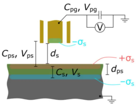
Figure S1. Schematics of the capacitive probe setup to measure surface charge density on flat samples.
As pictured in Figure S1, a circular brass probe with diameter 3/32 in. is maintained at 500 µm over the sample. The probe is shielded with a grounded casing. The sample is supported on a large brass plate connected to ground. The probe potential Vpg is measured with a high impedance electrometer (Keithley
6517A) with a 10 pF capacitor in the preamplifier feedback loop. A reference point is taken at the same height as the sample on a thin brass slab. The supporting plate is then displaced to the location of the sample to measure the difference in the potential profile, which is dependent on the surface charge density. Calibration is done by applying a known potential to the brass plate and measuring the voltage at the probe.
Using a parallel plate capacitance approximation for all capacitors, a probe of circular cross section (diameter: 3/32 in.), hovering 500 µm over the sample, yields a sensitivity factor S, such as σs = S Vpg, of
approximately 2.55 μF cm-2 for 230 nm oxide, and 6.51 μF cm-2 for 90 nm oxide. In this model, we neglected the thin polymer film on top of the oxide.
Determination of threshold voltage
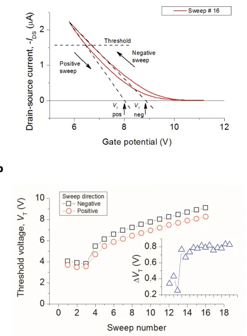
a
b
Figure S2. (a) Typical transfer characteristics showing how the threshold voltage is determined automatically. (b) Evolution of the threshold voltage as the device is swept. Inset: Evolution of the hysteresis ΔVT with respect to the sweep number.
As pictured in Figure S2(a), the threshold voltage VT is determined as the extrapolation to IDS = 0 from
the linear portion above a given threshold (typically 70% of the on-current) on the transfer
characteristics. The VT for both positive and negative-going sweeps can thus be extracted, and that, for
In the “on the fly” technique, VT is evaluated as stated by the custom Labview software for every sweep
[Figure S2(b)]. The as-determined VT then enters in the calculation of Qind, as explicated in the
“Methods” section of the main text. Doing so, we observe that VT will evolve at every sweep, but will
Additional Results
Annealing Step
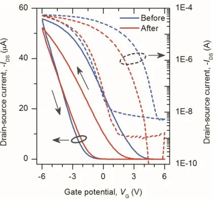
Figure S3. Comparison of the transfer characteristics before (blue) and after (red) the overnight annealing step at 200 °C under rough vacuum. Bare (not encapsulated) CNN-FETs built on SiO2/Si (Fraunhofer chips, Gen 5, 90 nm oxide). Channel dimensions:
20 × 2000 μm, VDS = -1 V. Solid lines: linear scale, dashed lines: semilog scale.
Figure S3 shows the transfer characteristics of a bare CNN-FET in ambient before and after the overnight annealing step at 200 °C under rough vacuum. Annealing under vacuum removes the loosely bound water molecules at the surface of the SiO2 layer, which consequently diminishes the amount of dioxygen
present at the CNT/SiO2 interface. It has for effect to lessen the p type doping due to the O2/H2O redox
couple.7 Therefore, hole conduction (p branch) decreases upon annealing as can be observed in Figure S3, as well as the off-state current. Removal of water molecules also decreases the hysteresis.
P2VP / PS Blends
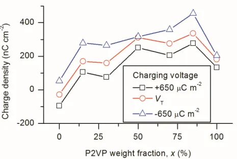
Figure S4. The charge density measured capacitively for various P2VP weight fractions in blends with PS. The data show three different charging voltages (Qind / Ceff = + 650 µC m-2 / Ceff, VT and Qind / Ceff = - 650 µC m-2 / Ceff).
Figure S5. Transfer characteristics of CNN-FETs encapsulated with P2VP-PS blends at various P2VP weight fractions. VDS = -3 V, VG = ± 650 µC m-2 / Ceff, channel dimensions: 20 µm × 2 mm.
a
b
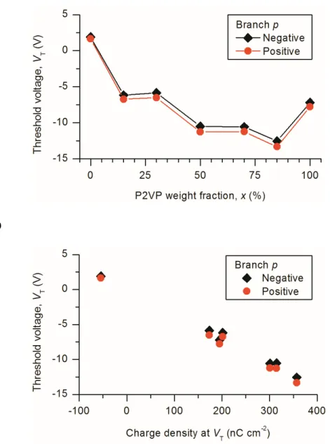
Figure S6. (a) The threshold voltage against the P2VP weight fraction in blends with PS. (b) The threshold voltage with respect to the charge density measured by the capacitive method. Negative and positive indicate the sweep direction.
a
b
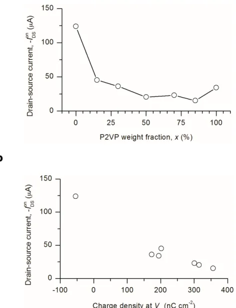
Figure S7. (a) The drain-source current as a function of the P2VP weight fraction in blends with PS. (b) The drain-source current with respect to the charge density measured by the capacitive method.
Figure S4 shows the measured charge density as a function of the P2VP weight fraction in blends with PS. We can see that charging the device at different applied potentials displaces the measured charge density for all P2VP weight fractions. The transfer characteristics were measured with dynamically adjusted VG limits and VDS = -3 V and are plotted in Figure S5. The displacement of VT and evolution of
Other Parameters Extracted from P(S-co-2VP) Copolymer Series
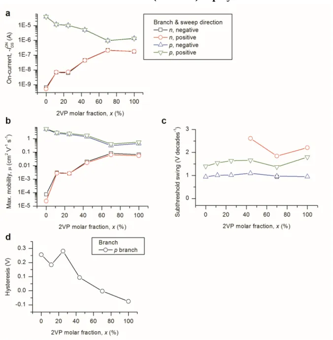
Figure S8. Other parameters extracted from the transfer characteristics measured for various 2VP mol%. (a) On-current. (b) Maximum mobility. (c) Subthreshold swing. (d) Hysteresis.
Supplementing the data regarding the P(S-co-2VP) copolymer mol% series presented in the main text, Figure S8 shows the evolution of other parameters that can be extracted from transfer characteristics. Notably, all of the parameters, to the exception of the subthreshold swing, can be tuned between their limit values by adjusting the 2VP molar fraction of the copolymer.
General Trends of Threshold Voltage against Various Charge States
Figure S9. The threshold voltage as a function of the charge density before cycling for encapsulated CNN-FETs.
Figure S10. The threshold voltage as a function of the charge density after grounding for encapsulated CNN-FETs.
Complementing Figure 3 in the main text, Figures S9 and S10 show the threshold voltage VT as a function
of the measured charge density at two different charging / discharging states. In Figure S9, VT is plotted
against the charge density as measured before any electrical contact is made with the sample. A fair linearity can be observed, but the scatter is more important that in Figure 3 (main text). In contrast, VT is
presented against the charge density as measured after grounding the sample in Figure S10. Interestingly, most of the data points are regrouped around 0 nC cm-2, with none being strongly
Additional Results of the Threshold Voltage against Charge Density at V
TFigure S11. (a) The threshold voltage as a function of the charge density after charging at VT for encapsulated CNN-FETs built on
top of 230 nm (red) and 90 nm (blue) SiO2 gate dielectric. The dashed lines correspond to the expected values from a parallel
plate model with the calculated oxide thickness-dependent capacitance, while the dotted lines correspond to Cao’s cylindrical model. (b) Comparison of different capacitor models. The experimental value of the capacitance per area is shown as the dashed-dotted green line. The dashed lines show the values computed from the parallel plate model for 90 and 230 nm gate oxide thicknesses. The full lines were calculated using Cao’s cylindrical model with the same parameters as above. The dotted vertical lines show the linear nanotube densities for which we calculated the cylindrical model at a given distance to match the experimental value at that density.
The red data points in Figure S11(a) corresponds to the same data as presented in Figure 3 of the main text, which belong to devices built atop 230 nm SiO2 dielectric. For comparison, data from devices built
atop 90 nm SiO2 dielectric are shown overlaid (blue triangles) in Figure S11(a). No meaningful offset could be measured, and the range of charge density of the 90 nm samples was not large enough to yield conclusions about the slope. For reference, dashed lines are traced from the Q = C · V relation where C is calculated from a parallel plate model with εr as the silicon dioxide value 3.9. Similarly, the dotted lines
take C from the cylindrical model by Cao et al. with CNT linear density Λ0-1 of 3.16 μm-1, quantum
capacitance CQ of 4.0 × 10⁻¹⁰ F m-1, CNT mean radius of 0.65 nm, and effective relative permittivity εr of
3.8,9 None of those two model yields an appropriate description of the measurements.
Figure S11(b) shows the extracted capacitance per area from the Figure 3 slope (28 nF / cm2) as the dashed-dotted green horizontal line. Similarly, the dashed blue and red horizontal lines represent the values for a parallel plate model with a separation of 90 and 230 nm SiO2, respectively. The plain blue
and red lines are for the cylindrical model by Cao et al. again with 90 and 230 nm SiO2, respectively, as a
function of the CNT linear density. We can thus see that the extracted capacitance per area cannot be reached by a capacitor formed by the back gate and the CNT film with a 230 nm oxide. Alternatively, we computed the cylindrical model capacitance per area for three different distances (0.39, 1.4 and 38 nm), such that it would match the extracted capacitance per area at CNT linear densities of 1, 3.16 and 10 μm-1, respectively.
Figure S12. The threshold voltage as a function of the charge density after charging at VT for encapsulated and bare CNN-FETs.
For comparison sakes, we have plotted in Figure S12 the measured VT as a function of the charge density
at VT for bare CNN-FETs on top of the data determined for encapsulated CNN-FETs. It is thus possible to
see that bare CNN-FETs inscribes themselves near the origin and do not generally diverge from the encapsulated measurements.
PVAc Thickness Series
Figure S13. Measured threshold voltage for a series of PVAc-encapsulated CNN-FETs with various thicknesses. Devices were built on 230 nm SiO2 with channels 10 µm × 2 mm. VDS= -3 V, Qind = ± 650 μC m-2.
In a further attempt to determine where the charges are located, we have tested a series of thicknesses using PVAc as the encapsulant. Solutions of different w/V concentrations were prepared in chloroform and spun cast on top of CNN-FETs with the same conditions, thus yielding PVAc layers with thicknesses varying according to the solution concentration. Subsequent measurement of the transfer
Comparing the Charge Density against Physical Parameters
Figure S14. The charge density measured after grounding the samples for various encapsulation dielectrics. (a) Versus the charge uptake after triboelectric contact.10 (b) Versus the pKb of an analog molecule to the polymer.10 (c) Versus the Gutmann’s
donor number of an analog molecule to the polymer.11
Following Diaz at al.’s correlation of triboelectric charge with basicity, we sought to compare the measured charge density of our layers with chemical parameters such as the pKb and Gutmann’s donor
number (DN). This could only be done for polymers where an appropriate analog molecule values could be found.10,11 In Figure S14(a), we first verify that there exists a loose correlation between the charge density measured in this work with the reported values for the triboelectric charge by Diaz et al.10 Furthermore, we also see general trends in Figures S14(b) and (c) when the charge density is plotted against either the pKb or the Gutmann’s DN, respectively, which emphasizes that the basicity of a
polymer encapsulant plays a role in the charge trapping effectiveness.
Comparative Results with N-DMBI / P2VP Encapsulated Devices
Figure S15. (a) Transfer characteristics of an uncapped CNN-FET device (1000 μm oxide) over time. (b) Transfer characteristics of a CNN-FET doped with N-DMBI and their evolution over time. Channel dimensions: 40 µm × 1000 µm. Gate oxide thickness: 1000 nm.
Supplementing the data presented in Figure 4 of the main text, we here show in Figures S15(a) and (b) the transfer characteristics as a function of time for the bare reference and N-DMBI n doped CNN-FETs,
and channel dimensions of 40 × 1000 μm. In Figure S15(a), we can thus see that the unprotected,
undoped device displays unipolar p type characteristics. They evolve during the period, presumably from p doping due to O2/H2O,7 with the on-current first increasing along with a concomitant decrease of the
on-off ratio. In comparison, the n doped device characteristics over time are shown in Figure S15(b). As doped, the device displays unipolar n type characteristics, which become stronger after an annealing step at 80 °C. The unipolar n type character is, however, rapidly lost as a strong p branch is present after only four days, which continues to grow as the dopant gets oxidized.
References
(1) CRC Handbook of Chemistry and Physic, 94th ed.; Haynes, W. M., Ed.; CRC Press: Boca Raton, 2016.
(2) Polymer Handbook, 4th ed.; Bandrup, J., Immergut, E. H., Grulke, E. A., Eds.; Wiley: New York, 2004.
(3) Bhattacharjee, B.; Das, H. L.; Goswami, T. D. DC Conductivity and Dielectric Constant of Cellulose Nitrate Detector. Radiat. Meas. 1995, 25 (1–4), 63–66.
https://doi.org/10.1016/1350-4487(95)00033-B.
(4) Zhang, S.; Painter, P. C.; Runt, J. Suppression of the Dielectric Secondary Relaxation of Poly(2-Vinylpyridine) by Strong Intermolecular Hydrogen Bonding. Macromolecules 2004, 37 (7), 2636– 2642. https://doi.org/10.1021/ma035830m.
(5) Davies, D. K. The Examination of the Electrical Properties of Insulators by Surface Charge Measurement. J. Sci. Instrum. 1967, 44 (7), 521–524. https://doi.org/10.1088/0950-7671/44/7/308.
(6) Secker, P. E. The Design of Simple Instruments for Measurement of Charge on Insulating Surfaces. J. Electrostat. 1975, 1, 27–36. https://doi.org/10.1177/109821409801900310.
(7) Aguirre, C. M.; Levesque, P. L.; Paillet, M.; Lapointe, F.; St-Antoine, B. C.; Desjardins, P.; Martel, R. The Role of the Oxygen/Water Redox Couple in Suppressing Electron Conduction in Field-Effect Transistors. Adv. Mater. 2009, 21 (30), 3087–3091. https://doi.org/10.1002/adma.200900550. (8) Schießl, S. P.; Rother, M.; Lüttgens, J.; Zaumseil, J. Extracting the Field-Effect Mobilities of
Random Semiconducting Single-Walled Carbon Nanotube Networks: A Critical Comparison of Methods. Appl. Phys. Lett. 2017, 111 (19), 193301. https://doi.org/10.1063/1.5006877. (9) Cao, Q.; Xia, M.; Kocabas, C.; Shim, M.; Rogers, J. A.; Rotkin, S. V. Gate Capacitance Coupling of
Singled-Walled Carbon Nanotube Thin-Film Transistors. Appl. Phys. Lett. 2007, 90 (2), 2005–2008. https://doi.org/10.1063/1.2431465.
(10) Diaz, A. F.; Felix-Navarro, R. M. A Semi-Quantitative Tribo-Electric Series for Polymeric Materials: The Influence of Chemical Structure and Properties. J. Electrostat. 2004, 62, 277–290.
(11) Cataldo, F. A Revision of the Gutmann Donor Numbers of a Series of Phosphoramides Including Tepa. Eur. Chem. Bull 2015, 4 (2), 92–97. https://doi.org/10.17628/ECB.2015.4.92.