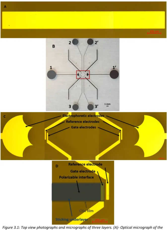
HAL Id: tel-02417045
https://tel.archives-ouvertes.fr/tel-02417045
Submitted on 18 Dec 2019HAL is a multi-disciplinary open access archive for the deposit and dissemination of sci-entific research documents, whether they are pub-lished or not. The documents may come from teaching and research institutions in France or abroad, or from public or private research centers.
L’archive ouverte pluridisciplinaire HAL, est destinée au dépôt et à la diffusion de documents scientifiques de niveau recherche, publiés ou non, émanant des établissements d’enseignement et de recherche français ou étrangers, des laboratoires publics ou privés.
Integration of a polarizable interface for electrophoretic
separation in a microfluidic device
Qiongdi Zhang
To cite this version:
Qiongdi Zhang. Integration of a polarizable interface for electrophoretic separation in a microfluidic device. Biophysics. Université Paris Saclay (COmUE), 2018. English. �NNT : 2018SACLS577�. �tel-02417045�
Integration of a polarizable
interface for electrophoretic
separation in a microfluidic device
Thèse de doctorat de l'Université Paris-Saclay
préparée à l’Université Paris-Sud
École doctorale n°575: Electrical, optical, bio-physics and engineering
(EOBE)
Spécialité de doctorat: électronique et optoélectronique, nano- et microtechnologiesThèse présentée et soutenue à Orsay, le 17 décembre 2018, par
Qiongdi Zhang
Composition du Jury: Philippe Lecoeur
Professeur, Université Paris-Sud (- Centre de Nanosciences et de Nanotechnologies-CNRS) Président
Gaëlle Lissorgues
Professeur, ESIEE Paris Rapporteur
Philippe Bergonzo V.P. Seki Diamond Systems
Professeur invité, University College London Rapporteur
Pierre Joseph
Chargé de Recherche, Laboratoire d’Analyse et d’Architecture des Systèmes-CNRS Examinateur
Wilfried Uhring
Professeur, Université de Strasbourg (- Laboratoire ICube) Examinateur
Ming Zhang
MCF, Université Paris-Sud (- Centre de Nanosciences et de Nanotechnologies-CNRS) Directrice de thèse
Anne-Marie Haghiri-Gosnet
Directrice de Recherche, Centre de Nanosciences et de Nanotechnologies -CNRS Co-encadrante
Antoine Pallandre
Professeur, Université Paris-Sud (- Laboratoire de Chimie Physique-CNRS)
Co-encadrant
NNT
:
2
0
1
8
S
A
CL
S
5
7
7
Université Paris-Saclay Espace Technologique / Immeuble Discovery
Route de l’Orme aux Merisiers RD 128 / 91190 Saint-Aubin, France
Titre : Intégration d’une interface polarisable pour la séparation électrophorétique dans un dispositif microfluidique
Mots clés : CNx, interface polarisable, transistor fluidique, microfluidique, flux électroosmotique Résumé : L’électrophorèse est une technique
puissante permettant de séparer des biomarqueurs présents dans les liquides biologiques. L’électrophorèse de zone libre transporte des molécules en milieu liquide sous l’influence de deux contributions : le flux électrophorétique et le flux électroosmotique (EOF). C’est ce dernier flux EOF qui permet d’optimiser la résolution analytique de la séparation et donc de simplifier le mélange avant sa détection. Notre équipe a développé un contrôle en temps réel de l’EOF en intégrant une interface polarisable diélectrique dans un dispositif microfluidique. Le carbone amorphe azoté (CNx avec x=15%) a été choisi comme ce matériau. Comme le CNx ne peut pas être déposé directement sur un substrat de verre à cause de sa faible adhérence, deux matériaux différents ont été proposés comme couche d’accroche : le carbure de silicium (SiC) et le platine (Pt). Nous avons tout d’abord optimisé l’adhésion entre le film CNx et la couche d’accroche SiC par différentes procédures
de fabrication. Cependant, en raison d’une faible adhérence, le film CNx s’est rapidement décollé en électrolyte liquide. Par contre, nous avons prouvé que certaines architectures hybrides incluant du Pt dans la couche d’accroche sont incroyablement robustes. Même après deux mois dans une solution millimolaire de KCl, le CNx adhérait toujours au verre sans aucune trace de délamination. Ce dispositif a fourni aussi une grande fenêtre de polarisabilité (de -1V à +1V). Nous avons enfin développé une architecture hybride « couche d’accroche isolée/couche électriquement polarisable /électrodes de grille enterrées/ polymère » afin d’éviter toute perte faradique dans l’électrolyte liquide ou vers les circuits conducteurs du dispositif. A l’issue de ces travaux, nous pensons être en mesure de proposer un composant fluidique complexe et robuste qui permet une modulation en temps réel de l’EOF lors de migrations électrophorétiques.
Title : Integration of a polarizable interface for electrophoretic separation in a microfluidic device Keywords : CNx, polarizable interface, fluidic transistor, microfluidic, electroosmotic flow
Abstract : Electrophoresis is currently an efficient way to separate precious biomarkers from complex mixtures. It takes place to transport molecules under two contributions: the electrophoretic flow and the electroosmotic flow (EOF). The latter allows to optimize the analytical resolution of the separation. Our team has developed a real-time dynamic control of the EOF by integrating a dielectric polarizable interface in the microfluidic device. Amorphous carbon nitride (CNx with x=15%) has dielectric properties and was chosen to be the polarizable interface. Since it cannot be deposited directly onto glass substrate, we have proposed and studied two different materials as the sticking underlayer: silicon carbide (SiC) and platinum (Pt). In the case of SiC, we have optimized the adhesion between CNx film and SiC underlayer through different fabrication procedures.
However, due to poor adhesion, CNx film delaminated into liquid electrolyte quickly. Compared to SiC, Pt is a good sticking underlayer for CNx. It was found out that even after two months in KCl solution, CNx still stuck robustly to Pt. Meanwhile, the device provided a large window of polarizability (from -1V to +1V). Finally, to avoid any faradic loss in the liquid electrolyte or towards the conductive circuitry of the device, we have developed a sticking underlayer/electrically polarizable/polymeric hybrid architecture. This architecture appears to be the most robust existing polarizable interface for strong and long-term adhesion onto glass substrates.
Acknowledgements
Firstly, I would like to thank all members of the committee: Mme. Gaëlle Lissorgues and M. Philippe Bergonzo who accepted to read my PhD manuscript and give advice; M. Pierre Joseph, M. Wilfried Uhring and M. Philippe Lecoeur who accepted to join my PhD defense and judge my work.
Secondly, I would like to give my sincere gratitude to my three supervisors: Mme. Ming Zhang who accepted me in this work and supported me behind all the time; Mme. Anne-Marie Haghiri-Gosnet who accepted me in a superb clean room to have experiments, guided my way forward and lit the pathway all along; M. Antoine Pallandre who was always be my technique advisor and my inspiring mentor, and who spent a lot of time on correcting my manuscript.
I am grateful to the clean room engineers who helped me a lot in the microfabrication and gave me so much useful advice, they are M. Abdou Harouri and M. Laurent Couraud. I would like also express my deep appreciation to my friends and colleagues for their support and comprehension: Xuan, Fatima, Alisier, Julie, Mery, Lyas, and Bacem. All the members of my team and the C2N clean room are also deeply acknowledged for their kind guidance.
Thank you ANR Labex LaSIPS for the financial support. And thank you C2N for the facilities and equipment support.
And last but by no means least I would like to express my deepest love to all my family members, to whom have always been there for me: Mum, Dad, Meemaw, and Cheri, your continuous support has made everything possible for me.
Abstract
Medical check-up and diagnostics require multiplexed sample treatments and high-resolution separations. After the separation steps, a sensitive detection of the biomarkers has to be carried out. One way to efficiently separate precious biomarkers from complex mixtures that are currently used by biochemists is electrophoresis. Electrophoresis takes place to transport molecules under two contributions: the electrophoretic mobility that is directly related to the ratio between weight and charge of molecules and the electroosmotic mobility that allows to optimize the analytical resolution of the separation. Most of the time analysts modulate electroosmotic flow (EOF) by adjusting pH of solution, or changing the ionic strength of buffer, or just using surface treatments. All these methods aim to tune the electrostatic charge state of the solid/liquid interface and to limit unspecific adsorption inside the microfluidic channel. However, these strategies cannot lead to real-time surface charge adjustment. Therefore, in our microfluidic transistor, a dielectric polarizable interface is integrated in order to achieve a dynamic control of the EOF. Such polarizable gate allows a real-time modulation of the zeta potential at the solid/liquid electrolyte interface under the application of low voltage. This fluidic transistor with its integrated gate voltage is thus engineered for a fast and efficient control of EOF independently from the electrophoretic field. Amorphous carbon nitride (CNx with x=15%) has been chosen to be the dielectric polarizable material for the gate. Since the CNx cannot be deposited directly on glass substrate, two different materials have been proposed and studied as sticking underlayer: silicon carbide (SiC) and platinum (Pt). In this work, we have studied the behavior of CNx film deposited on these two different materials for different architectures of the device. Due to poor adhesion between CNx and SiC, CNx film quickly delaminated into the liquid electrolyte. Compared to SiC, Pt is a good sticking underlayer for CNx that was found to be incredibly robust. Even after two months in KCl solution, CNx still adhered to Pt without any delamination. Moreover, to avoid any faradic loss in the liquid electrolyte or towards the conductive circuitry of the device, we have developed a hybrid architecture with polymeric insulating pads at the two extremities of the CNx gate electrode. This sticking layer/electrically polarizable/polymeric hybrid architecture appears to be the most robust existing polarizable interface for strong and long-term adhesion onto glass substrates.
I
Contents
Chapter 0: General Introduction ... 1
REFERENCES: ... 2
Chapter 1: Background Introduction ... 3
1.1. Overview ... 3
1.2. Microfluidic Separation ... 3
1.2.1. Capillary Electrophoresis ... 3
1.2.2. Electroosmotic Flow and Zeta-Potential ... 5
1.3. Flow FET and Microfluidic Wheatstone Bridge ... 9
1.3.1. From MIE-FFET to PI-FFET ... 9
1.3.2. Microfluidic Wheatstone Bridge ... 12
1.3.3. Polarizable Interface and Polarizability Window ... 16
1.4. Conclusions ... 17
REFERENCES: ... 17
Chapter 2: Simplification of EOF Measurement Equipment ... 23
2.1. Overview ... 23
2.2. Theoretical Analysis ... 24
2.2.1. Adder ... 24
2.2.2. Voltage Follower ... 25
2.2.3. Regulator ... 26
2.3. Simulation, Fabrication and Experimental Validation ... 26
2.3.1. Simulation ... 27
2.3.2. PCB Fabrication ... 29
2.3.3. PCB Experimental Validation ... 30
2.4. Conclusions ... 32
REFERENCES: ... 32
II
3.1. Overview ... 34
3.2. Step-by-Step Fabrication Processes for Microfluidic Devices ... 36
3.2.1. Typical Microfabrication Processes of PI-FFET on Glass Substrate ... 36
3.2.2. Two Microstructuring Methods of Microfluidic Channels ... 41
3.2.3. Integration of PI-FFET and Microchannels ... 44
3.3. Description for Experimental System ... 45
3.3.1. Experimental Bench ... 45
3.3.2. Step-by-Step Experimental Description ... 46
3.4. Conclusions ... 49
REFERENCES: ... 50
Chapter 4: Experimental Work ... 55
4.1. Overview ... 55
4.2. Experiment 1: Insulating SiC Sticking Underlayer and Its Adhesion Optimizations ... 55
4.2.1. Aims of Experiment 1 ... 55
4.2.2. Experiment 1.1: Choice of SiC as Sticking Underlayer ... 55
4.2.3. Experiment 1.2: Adhering Optimization by Short Piranha Treatment ... 61
4.2.4. Experiment 1.3: Adhering Optimization by Investigating CNx Deposition Conditions ... 70
4.2.5. Experiment 1.4: Adhering Investigation by Introducing Post-annealing after CNx Deposition ... 73
4.2.6. Experiment 1.5: Sheet Resistance Measurements of CNx by 4-point Probes Method 75 4.2.7. Experiment 1.6: First Measurement of EOF and Polarizability Window ... 76
4.2.8. Conclusions ... 78
4.3. Experiment 2: Choice of Metallic Pt as Sticking Underlayer ... 79
4.3.1. Aims of Experiment 2 ... 79
4.3.2. Experiment 2.1: Amazing Adhering Aging of Pt as Sticking Underlayer ... 79
III
4.3.4. Conclusions ... 90
4.4. Experiment 3: New Role of CNx — An Insulating Layer ... 90
4.4.1. Aims of Experiment 3 ... 90
4.4.2. Experiment 3.1: Isolation and Polarization Together in One-Layer CNx ... 90
4.4.3. Experiment 3.2: Isolation and Polarization Separated in Two-Layer CNx ... 93
4.4.4. Conclusions ... 95
4.5. Experiment 4: Innovative Configuration Avoiding Any Unwanted Electric Contact and CNx Detachment ... 95
4.5.1. Aims of Experiment 4 ... 95
4.5.2. Experiment 4.1: Employment of Absolutely Insulating Si3N4 Material ... 95
4.5.3. Experiment 4.2: Employment of Relatively Insulating SiC Material ... 98
4.5.4. Conclusions ... 99
4.6. Conclusions ... 100
REFERENCES: ... 100
V
Abbreviations
AC alternating current AFM atomic force microscopy CCD charge-coupled device CE capillary electrophoresis COC cyclic olefin copolymer COP cyclic olefin polymer DC direct current
EBPVD electron-beam physical vapor deposition EDL electrical double layer
EDS energy-dispersive X-ray spectroscopy EOF electroosmotic flow
EP electrophoresis FET field effect transistor FFET flow field effect transistor HMDS hexamethyl disilazane
HPCE high performance capillary electrophoresis IC integrated circuit
IPA isopropyl alcohol LOC lab-on-a-chip
MEMS micro-electro-mechanical systems MIE metal-isolator-electrolyte
µFWB microfluidic Wheatstone bridge µTAS micro total analysis system NEMS nano-electro-mechanical systems
VI
Opamp operational amplifier PC polycarbonate PCB printed circuit board PDMS poly (dimethyl siloxane) PEEK polyether-ether-ketone PET poly (ethylene terephthalate) PI polarizable interface
PIA particle image anemometry PMMA poly (methyl methacrylate) POC point-of-care
PS polystyrene PVC polyvinyl chloride
PVD physical vapor deposition RF radio frequency
RIE reactive-ion etching ROI region of interest RPM revolutions per minute UV ultraviolet
1
Chapter 0: General Introduction
For decades, benefitting from the advances in micro-electro-mechanical systems (MEMS), nano-electro-mechanical systems (NEMS) and integrated circuit (IC) industries technologies, microfluidic technology has become an important tool for chemical, biological and medical researches. Meanwhile, capillary electrophoresis (CE) is a high-performance separation method for those analytical studies in liquid. One way to further improve this analytical method concerns the ability to control the electroosmotic flow (EOF) that competes with the electrophoretic flow. To achieve a dynamic real-time manipulation of the EOF, a gate electrode that is similar to the gate in electronics was integrated into a microfluidic device, called “flow field effect transistor” (FFET) [1]. Researchers have then developed different FFET variants. Among them, our team designed a polarizable interface FFET (PI-FFET) that integrated a polarizable material (CNx) as the gate of the device [2]. On the other hand, printed circuit board (PCB) technology has greatly reduced the space and weight of ICs. By combining a functional PCB with the PI-FFET device, it will be one day possible to realize a portable, space-saving, efficient and mass-production microfluidic separation analytical device. Before that, an urgent problem to be solved concerns the robustness of the transistor itself. In contact with aqueous liquids we observed delamination of the PI from the substrate. Indeed, the older generation of PI-FFET lasted no more than ten days. It is too short and its performances were not reliable after few days. In other words, the choice of the building materials and the architecture of the PI-FFET has to be fully thought over and it was the aim of this project.
Amorphous carbon nitride (CNx with x = 15%) as a dielectric polarizable material has rarely been studied to be integrated in a complex microfabricated device. As a pioneer to use such a material as gate material, along my PhD work, I have studied the way to improve its adhesion ability to the glass substrate. I have thus studied the roles of various factors of environment, of the fabrication process and of the material itself on CNx adhesion stability. I have also developed specific fabrication processes to integrated at the glass/CNx interface different underlayers.
The whole manuscript is divided into five sections.
Chapter 1 mainly introduces the background of microfluidic separation and the methods to improve it. The first Flow FET device is described as well as the birth of our PI-FFET device. Chapter 1 also gives a glance at the design structure and the EOF measurement method of the PI-FFET.
Chapter 2 simply presents a simplification of the EOF measurement equipment. It was done during the 1st year of my PhD to replace two classical electronic voltage followers by a small light printed circuit
board (PCB). Theoretical analysis, design and simulation, as well as fabrication and experimental validation of this PCB card are presented successively.
Chapter 3 illustrates the whole fabrication process of PI-FFET device and the whole experimental bench set-up in detail.
2
Chapter 4 reports all my experimental studies with the three different configurations of the PI-FFET, each of them performing various testing to improve progressively CNx adhesion.
Chapter 5 as the last section gives a concise conclusion of my three-year PhD thesis work. I also add recommendations for future work.
R
EFERENCES:
[1] R. B. M. Schasfoort, S. Schlautmann, J. Hendrikse, and A. van den Berg, “Field-effect flow control for microfabricated fluidic networks,” Science, vol. 286, pp. 942-945, 1999.
[2] A. Plecis, J. Tazid, A. Pallandre, P. Martinhon, C. Deslouis, Y. Chen, and A-M. Haghiri-Gosnet, “Flow field effect transistors with polarizable interface for EOF tunable microfluidic separation devices,” Lab Chip, vol. 10, pp. 1245-1253, 2010.
3
Chapter 1: Background Introduction
1.1. Overview
In this chapter, the background around separation using electrophoresis is given as introduction. First of all, capillary electrophoresis is presented, in which the electroosmotic flow (EOF) plays an important role. Second, two major concepts related to the EOF, (i) the surface charge and (ii) the electrical double layer are presented successively. It allows us to define the zeta-potential, an essential factor for electroosmotic phenomenon. By controlling this zeta-potential, analysts can manipulate the EOF in order to better control separation and its resolution. Later, a dynamic mode to control zeta-potential, the first Flow Field Effect Transistor (FFET) designed by a team in Netherlands, is discussed and followed by an introduction of our polarizable interface FFET, which overcomes some disadvantages of the previous one. At the end of this chapter, an H-shaped microfluidic Wheatstone bridge (µFWB) device is presented in detail.
1.2. Microfluidic Separation
As indicated by its name, microfluidics is a technology that manipulates small amounts of fluids (10-9
to 10-18 L) in channels with dimensions from tens to hundreds of micrometers [1, 2]. It has been widely
used during the last tenth years for various applications: chemical analysis, molecular analysis, biodefence, molecular biology, medical diagnosis, even microelectronics engineering, and etc. [2-4]. By integrating microfluidic components onto a single chip, it has contributed to advances of lab-on-a-chip (LOC) devices [5], micro total analysis system (µTAS) [6], and point-of-care (POC) diagnostic devices [3, 7]. In a word, microfluidics provides a rapid, efficient, inexpensive, and portable way for universal analysis.
Microfluidic handling on-a-chip consists of sample preparation (including purification, preconcentration and labeling), separation, and detection [8]. In the field of separation based on microfluidic system, various techniques have been developed and explored [9, 10]. For example, continuous hydrophoretic techniques [8], such as gel electrophoresis [11, 12] and electrophoresis [13-17]; and utilized external force techniques [18], like acoustophoresis [19-24], dielectrophoresis [25-32], magnetophoresis [33-38], mechanical forces [39-42], and optophoresis [43-45]. In my thesis, I will mainly present the free zone capillary electrophoresis separation and its improvement by a better control of the electroosmotic flow.
1.2.1. Capillary Electrophoresis
Before introducing more specifically free zone electrophoresis on-a-chip, let us briefly understand what is the general principle of electrophoresis from an experimental point of view. Under the application of an electric field, the charged particles move towards the electrode of opposite charge, so it is called electrophoresis. The electrophoretic phenomenon was first discovered by Russian professor F.F. Reuss at Moscow State University in 1807 [46]. Electrophoretic technique uses different moving velocities of charged particles in an electric field to achieve their separation. This method was invented by a Swedish researcher A.W.K. Tiselius in 1936. He designed and manufactured a moving
4
boundary electrophoresis instrument “Tiselius apparatus” that separated successfully three kinds of globulins from serum albumin of horse [47].
Capillary electrophoresis (CE), also called high performance capillary electrophoresis (HPCE), is a new type of liquid phase electrokinetic separation technology with submillimeter diameter capillaries as separation channels and high voltage DC electric field as driving force. Nowadays, miniaturized CE technology has already attracted lots of attentions. It has been used in various fields in laboratories and industries, owing to its fabulous advantages, such as its portability, low cost, reduction of sample consumption, fast analysis, and low voltage power supply [48]. So, how does the separation in miniaturized CE system happen?
Figure 1.1: Two opposite forces acting on a positive ion as it moves through a microfluidic channel, subjected to an electric field.
Figure 1.1 shows a positive ion placed in microfluidic channel under the influence of an electric field. Two forces act on the ion: the electrophoretic driving force Fep that is given by the product of the ion valence z, elementary charge e, and electric field strength E, as shown in Formula 1-1:
𝑭𝒆𝒑= 𝑧𝑒𝑬 (1-1)
and the Stokes’ drag force Fdrag that is opposite to the former [49]. According to the Stokes’s law, it is described as Formula 1-2:
𝑭𝒅𝒓𝒂𝒈= −6𝜋𝜂𝑟𝒗𝒆𝒑 (1-2)
where η is the fluid viscosity, r is the effective radius of the ion, vep is the electrophoretic migration velocity. It should be noted that in this model the ion is a small spherical particle and it moves at a steady state velocity after a short period in a laminar flow.
For aqueous solutions containing ionic compounds, for example KCl salt in water, ion hydration always occurs. Ion hydration refers to a physical interaction between an ion and a neutral molecule that has a dipole, essentially as an electrostatic attraction: a cation attracts the partially negative end of a neutral polar molecule (K+ with oxygen atom of water molecule), while an anion attracts the partially
positive end (Cl- with hydrogen atom of water) [50]. There are two combination methods of ion-dipole
interaction: either in the form of ion pairs, or one ion surrounded by a tightly bound atomic layer of several water molecules. Due to this, the effective radius of the ions is not the ionic radius but the hydrated radius.
After a few microseconds, the two forces are balanced, i.e. Fep + Fdrag = 0, thus the ion moves at a constant velocity. Then the electrophoretic migration velocity is obtained as shown in Formula 1-3:
5
𝒗𝒆𝒑= 𝑧𝑒𝑬
6𝜋𝜂𝑟 (1-3)
Since vep can also be expressed by the product of the mobility and electric field strength, then the electrophoretic mobility can be given as Formula 1-4:
µ𝑒𝑝= 𝑧𝑒
6𝜋𝜂𝑟 (1-4)
From Formula 1-3 and 1-4, it can be seen that both the electrophoretic velocity and mobility are proportional to the ionic charge, and inversely proportional to the hydrated radius, i.e. relating to the ionic radius, considering that the fluid viscosity and the electric field strength are fixed. Therefore, when different ionic species migrate through the same solution and are subjected to the same electric field, due to different sizes and charges of particles, they have different mobilities, i.e. different velocities, and eventually they separate. Except this electrophoretic velocity, there is another velocity in CE system that should be considered, the electroosmotic flow (EOF) of the buffer solution.
1.2.2. Electroosmotic Flow and Zeta-Potential
Before introducing EOF, let us first familiarize with two concepts: the surface charge and the double layer.
Figure 1.2: Model of the EDL for fused-silica based substrate. The first compact layer is the Stern layer, the second diffuse layer is the Gouy-Chapman layer. Together, they form the electrical double
layer.
When a solid contacts to a liquid, its surface is not always neutral. Depending on the solid property and pH value of liquid, the surface could be positively or negatively charged. It is called surface ionization. Let us describe for example the case of fused-silica capillary, the material commonly used in CE system. When it is filled with a buffer solution at pH value greater than three, the silanol (Si-OH) groups that attach to the interior wall of capillary are ionized to negatively charged silanoate (Si-O-)
groups [51]. This kind of surface ionization in capillary can be enhanced by flushing basic solution such as NaOH or KOH through the channel before introducing buffer solution [52].
In the case mentioned-above, the cations of the buffer solution will be attracted to those negatively charged silanoate groups, and then form a compact inner layer on the capillary interior wall, which is also called “Stern layer” or compact layer. Because the density of cations at the inner layer is not large enough to neutralize all the negative charges on the capillary surface, an outer diffuse layer is formed by cations and a few anions [53]. This layer is also called “Gouy-Chapman layer” or mobile layer. Thus, a diffuse double layer, i.e. electrical double layer (EDL) is formed, as represented in Figure 1.2.
6
The first EDL model was proposed by Helmholtz in 1853 [54]. In his model, the EDL was considered as a monolayer with counter ions on the surface and the potential dropped rapidly across the EDL. This model was too simple to explain the electrokinetic phenomenon. Later in the year between 1910 and 1913, Gouy and Chapman improved Helmholtz’s model and proposed the Gouy-Chapman model [55, 56]. It was the first time that the diffuse layer was introduced in EDL, and the potential dropped in an exponential way. In 1924, Stern combined the two previous models and then introduced a double-layer in the EDL [53]. The first double-layer was called “Stern double-layer”, as already mentioned above. In this double-layer, the change of potential was similar to the one in the Helmholtz model, while the second layer was similar to the diffuse layer in the “Gouy-Chapman” model, in which potential varies in an exponential way. The potential between these two layers was referred to as the zeta-potential.
In an electric field, the cations inside the mobile layer are pulled in the direction of cathode. Due to the ion hydration, also said ion solvation, when solvated cations move, they take along the surrounding water molecules, dragging the bulk buffer solution migrating together with the mobile layer due to the frictional forces [57, 58]. This dragging flow is called the electroosmotic flow. It is believed that EOF occurs due to the interaction between the charged ions on the surface of channel and the buffer solution [59].
The electroosmotic mobility can be defined by the Smoluchowski equation [60], as shown in Formula 1-5:
µ𝑒𝑜𝑓= 𝜀0𝜀𝑟𝜁
𝜂 (1-5)
where ε0 is the permittivity of vacuum, εr is the relative permittivity of the buffer solution, ζ is the
zeta-potential. As the electroosmotic velocity is the product of its mobility and the electric field strength, similar to Formula 1-3, thus, it can be described as Formula 1-6 as follow:
𝒗𝒆𝒐𝒇 = µ𝑒𝑜𝑓𝑬 = 𝜀0𝜀𝑟𝜁𝑬
𝜂 (1-6)
By combining the electrophoretic migration and the electroosmotic migration, Formula 1-7 shows the effective velocity of an analyte in an electric field:
𝒗𝒆𝒇𝒇= 𝒗𝒆𝒑+ 𝒗𝒆𝒐𝒇= (µ𝑒𝑝+ µ𝑒𝑜𝑓)𝑬 = ( 𝑧𝑒 6𝜋𝜂𝑟+
𝜀0𝜀𝑟𝜁
7
Figure 1.3: Velocity profiles for the pumped flow (left) and the electroosmotic flow (right).
The velocity profile of EOF is different to the pressure-driven laminar flow (Poiseuille flow), as shown in Figure 1.3. Compared to the latter, the EOF profile is flat, plug-like, and has narrow band-broadening. That means, it has less variation in its velocity profile when passing through the detection window. This is a great advantage for CE system because all pressure differences during electrophoretic separation should be eliminated at thus limits the band-broadening coming from the laminar parabolic profile [61, 62]. The resolution factor Rs gives a link between EOF and the quality of separation, as
described in Formula 1-8 [63, 64]:
𝑅𝑠= 𝐴
(µ𝑎−µ𝑏)
√(µ𝑎+µ𝑏)/2−µ𝑒𝑜𝑓 (1-8)
where A is a constant, µa and µb are electrophoretic mobilities of two analytes injected in the
microchannel. This formula quantifies the ability to distinguish two successive peaks of analytes that the electroosmotic mobility µeof fits to the averaged electrophoretic mobility of the analytes [63, 64].
Figure 1.4: The order of EOF separation of charged and neutral analytes in a fused-silica capillary channel according to their size and electrical charge.
Since electroosmosis often occurs along with electrophoresis, and the EOF of buffer solution is generally five to seven times greater than the electrophoretic flow of analytes, as long as the channel is long enough, all analytes can be separated in the end. Figure 1.4 illustrates the separation. Assuming in fused-silica capillary, cations move towards the cathode and can be separated firstly with the aid of
8
the EOF, whereas anions move back towards the anode, counter to the EOF, thus separated at last. The multiply charged cations migrate most quickly while the multiply charged anions migrate most slowly. The neutral analytes have no electrophoretic mobility so they move with buffer solution driven by EOF mobility and are separated after cations. Therefore, a separation of sample is achieved. It should be noted that only the electrophoretic force acts to separate analytes.
Figure 1.5: Possible reasons for EOF instability (image derived from [65]).
Modulation of the EOF allows optimizing a high analytical resolution separation that outperforms the traditional free zone CE [63, 64]. However, control of the EOF is not easy, since it depends on several parameters. Figure 1.5 presents those possible reasons that may affect the EOF [65]. It can be seen that the instability of the EOF comes from two main factors: the zeta-potential and the viscosity. The latter depends on the temperature and buffer composition, which is normally stable as long as the power is not too high. While the former, greatly depending on surface charge, is the key role to be manipulated. It should be noted that despite buffer concentration being another important factor for the zeta-potential, however, it can be easily kept constant [65]. Besides, working with low buffer concentration has few influences on the change of the absolute permittivity (product of the permittivity of vacuum and the relative permittivity as shown in Formula 1-5), i.e. the dielectric constant [65]. Therefore, the optimization and enhancement of separation resolution is dominated by the zeta-potential, i.e. the charge density of the channel wall. Several methods have been reported to adjust pH value of buffer solution [66-68], and to modify buffer solution [66, 69]. Analysts also used surface treatments such as polymer coating, self-assembled monolayer, etc. [70, 71]. However, all of these methods are non-dynamic and they are optimized for one kind of separation. Thus, scientists started to find a dynamic method to modify the zeta-potential by using an external electric field [72, 73].
9
1.3. Flow FET and Microfluidic Wheatstone Bridge
In 1999, the team of A. van den Berg first developed a microdevice named “flowFET” [72]. The interest was to control variation of zeta-potential in real time by adding an external gate electrode. They were able to generate electric field strength of 1.5x10⁸ V/m by applying a voltage of 50V over the channel.
And they also demonstrated a greater control of EOF at lower pH values of 3.5 and 4.5. Later in 2005, the same team improved the Flow FET (FFET) device to stop and even reverse the direction of EOF, and they showed an almost linear relation between the applied gate voltage and zeta-potential [73]. Based on their concept, our team has also proposed and developed a novel FFET microdevice with an electrically polarizable interface in direct contact with the electrolyte [64]. This configuration allowed a control of zeta-potential under several volts, thus at very low gate voltages compared to previous results, probing thus the concept of EOF control by polarizable interface.
1.3.1. From MIE-FFET to PI-FFET
Figure 1.6: The classical MIE-FFET. (A)- The configuration. (B)- The simplified model of EDL. (C)- The three-capacitor model representing the substrate/electrolyte interface. From (A) to (C): images taken
from [64]. (D)- The photograph of two MIE-FFETs integrated with a channel junction (left) and the SEM image of this channel junction (right), images taken from [72]. (E)- The photograph of the final
10
Figure 1.6A shows the configuration of the conventional metal-insulator-electrolyte (MIE)-FFET [64]. It can be seen that this configuration is analogous to that of the solid-state field-effect transistor (FET) in microelectronics, where the perpendicular field generated by the gate electrode manipulates electric current. In this layout, the two electrodes at the both ends of channel play similarly to the source and drain electrodes in FET and the third gate electrode attached to the outside of the channel wall manipulates the EOF [72]. Noted that Vgate is the applied gate voltage and Vext is the external transverse
voltage, i.e. electrophoretic voltage to perform electrophoresis. In this single gate electrode configuration, a non-homogeneous surface charge distribution along the x-axis is observed. The simplified model of EDL of the MIE-FFET is presented in Figure 1.6B [64]. Its corresponding three-capacitor model is represented in Figure 1.6C [64]. Here, V is the gate electrode potential depending on applied gate voltage Vgate, Ψ is the surface potential of the insulator surface, φ is the electrolyte
potential. The potential distribution in the insulator can be represented as a linear drop across it, which means that the field effect is proportional to the insulator thickness and to Vgate.
The three capacitances are: Ci capacitance of the insulator; Cs capacitance of the Stern layer; and Cedl
capacitance of the EDL. The value of Ci can be approximated by Formula 1-9:
𝐶𝑖= 𝜀0𝜀𝑟𝐴
𝑑 = 𝜀𝐴
𝑑 (1-9)
where ε is the absolute permittivity of material, i.e. the dielectric constant, A is the electrode area, and d is the thickness of the insulating layer. It is undoubted that the thicker the layer is, the lower is its capacitance. The Stern capacitance is often neglected because it is only significant in the electrical circuit for solutions with large electrolyte concentrations or for dilute media with large polarization [73]. Besides, it is much larger than Ci and Cedl since the Stern layer has only a few Å and the EDL has a
few tens of nanometers, while insulator is much thicker (Cs > Cedl > Ci) [64, 72]. The value of Cedl can be
simplified and described by Formula 1-10 [73, 74]:
𝐶𝑒𝑑𝑙 = 228𝑧√𝑐 cosh(19.5𝑧𝜁) (1-10)
where z is the ion valence, c is the electrolyte concentration. This formula is only valid for dilute aqueous solutions at 25°C.
Therefore, the variation of zeta-potential can be induced by the gate voltage Vgate as given in Formula
1-11 [73]:
𝛥𝜁 = 𝐶𝑖
𝐶𝑒𝑑𝑙 (𝑉𝑔𝑎𝑡𝑒− 𝜑) (1-11)
From the Formula 1-11, it is clear that the zeta-potential variation is proportional to the insulator capacitance and the gate voltage, and inversely proportional to the EDL capacitance. Taking account of Ci, its increase corresponds to a high dielectric constant for a very thin insulator. Meanwhile, to keep
the gate voltage low, an extremely thin wall (<1 µm) is also required [72]. Thus, the insulating material should have a high value of electrical breakdown strength. However, considering about Cedl that also
depends on zeta-potential, the relation between Δζ and Vgate is more complicated.
Figure 1.6D and E exhibit the photographs of the first MIE-FFET device (Figure 1.6D) and the second improved device (Figure 1.6E) respectively. These devices have demonstrated ability to control the
11
zeta-potential by tuning the external perpendicular gate field, resulting in a fast and dynamic manipulation.
Figure 1.7: The PI-FFET developed by our team. (A)- The configuration. (B)- The simplified layout of EDL. (C)- The two-capacitor model representing the substrate/electrolyte interface. (D)- The
photograph of the final device. Images taken from [64].
Figure 1.7 shows the polarizable interface based FFET designed by our team and called PI-FFET [64]. Its configuration is illustrated in Figure 1.7A. As it can be seen, there is no insulator; the commanded layer is directly immerged into the electrolyte. The control of zeta-potential is achieved by applying a potential difference between these two layers. This potential difference between the electrolyte potential φ and the control gate electrode V is called over-potential γ (= V-φ), and the variation of γ (Δγ) allows the variation of zeta-potential (Δζ). To get such Δζ, the commanded layer should be polarizable, called “polarizable interface”.
Figure 1.7B and C represent the simplified layout of the PI-FFET configuration and its two-capacitor model respectively [64]. Since there are no insulating layer, the surface potential is equal to the gate electrode potential (Ψ = V). Meanwhile, there is no more insulator capacitance Ci. Thus, the variation
of induced zeta-potential can be given as Formula 1-12 [64]: 𝛥𝜁 (𝛾) = 𝐶𝑠
𝐶𝑠+𝐶𝑒𝑑𝑙(𝛾) (1-12)
Due to the Stern capacitance that is larger than EDL capacitance, the Formula 1-12 can be simplified and approximated by Formula 1-13 [64]:
12
𝛥𝜁 (𝛾) ≈ 𝛾 (1-13) Since the over-potential is controlled by applying a voltage difference with the nearest external electrode called ΔVgate, the Formula 1-13 can be modified by Formula 1-14 [64]:
𝛥𝜁 (𝑥) ≈ 𝛥𝑉𝑔𝑎𝑡𝑒 (1-14)
which means, as long as the gate voltage remains within the admissible potential window, the zeta-potential, i.e. the manipulation of EOF only depends on the experimental gate voltage, the external longitudinal electric field is independent to this control and does not influence it, so as to the other factors.
Based on this concept, our team has designed, fabricated and experimented the PI-FFET device, as shown in Figure 1.7D. Compared to the MIE-FFET, PI-FFET overcame the difficulties met with the former: as dual gate electrodes integrated at both ends of channel wall, the surface charge along the channel is more homogeneous; as no insulator existing in PI-FFET, there is no risk of breaking the insulator (insulating layer becomes porous and current leakages occur with the MIE-FFET configuration); as the ratio of the insulator capacitance to the EDL capacitance is very small (cause of layer thickness), MIE-FFET requires large gate voltage according to Formula 1-11. With this PI-FFET device, our team has successfully tuned zeta-potential in a large potential window with very low gate voltages from -2V to +2V [64].
1.3.2. Microfluidic Wheatstone Bridge
Figure 1.8: The analogy of microflows to electrical currents. (A)- Pressure-driven Poiseuille flow and its analogy to electrical current. (B)- Electroosmosis-driven plug-like flow and its analogy to electrical
13
The measurement of EOF in such a PI-FFET device is performed by using a H-shaped fluidic network, called “microfluidic Wheatstone bridge (µFWB)”, a configuration designed by our team more than a decade ago [75]. The conception was inspired based on an analogy of microflows to electrical currents as shown in Figure 1.8 [63].
There are two typical flow profiles existing in rectangular microchannels: the Poiseuille flow and the electroosmotic flow. The former is a pressure-driven flow with a parabolic velocity profile, which can be seen in Figure 1.3. This kind of flow is valid at low Reynold’s number (laminar flows). It can thus be considered as incompressible Newtonian fluid and the average flow rate J can therefore be expressed by Navier-Stokes equations [76]. The analogy of Poiseuille flow to electrical current can be illustrated as shown in Figure 1.8A [63]. The pressure P1 generated by pumps or syringe can be considered as a
voltage source, the mass P0 can be equivalent to the atmospheric pressure, the flow rate J corresponds
to the generated current. In this case, there is no electric field thus no electrical current injected across the channel. The second flow is the electroosmosis-driven flow with a plug-like velocity profile (see Figure 1.3). The analogy of electroosmotic flow to electrical current is displayed in Figure 1.8B [63]. There is no driven pressure, the electroosmotic flow can thus be modeled by a current source, producing a flow rate J (the EOF Jeof) that only depends on zeta-potential ζ and injected electrical
current I, as described by Formula 1-15 [75]:
𝐽𝑒𝑜𝑓 = 𝜎 𝜀0𝜀𝑟𝜁
𝜂 𝐼 (1-15)
where σ, ε0εr and η is the conductivity, permittivity and viscosity of the solution respectively that
normally do not change. Figure 1.8C shows the superimposition of Poiseuille flow and EOF, in which the total flow rate is the sum of two, resulting in a zero-net flow. As the outlet is plugged (like open switch in electrical system), a counter flow Jp is generated. Due to the mass conservation, Jp = -Jeof [63].
14
Figure 1.9: The analogy of µFWB to electrical Wheatstone bridge. (A)- The general analogy. (B)- The analogy in EOF mode, under electric field, leading to the fluidic resistance calibration. (C)- The analogy in Poiseuille mode without electric field, leading to the Poiseuille calibration. Image taken
from [63].
Based on the above analogy, our H-shaped µFWB system was designed as shown in Figure 1.9 [63]. The left figure in part A shows the configuration of the H-shaped µFWB device, Figure 1.9A illustrates the analogy between the µFWB and the electrical Wheatstone bridge.
15
Before measurements of EOF, two calibrations should be done. These calibrations are shown in Figure 1.9B and C respectively [63]. When an electric field is applied in the central channel (part B), the generated EOF causes four Poiseuille flows in four arms (side channels), proportional to the EOF flow rate Jeof, following Formula 1-16 [75]:
𝐽𝑒𝑜𝑓 = 𝛼𝑖𝐽𝑖 (𝑖 = 1,2,3,4) (1-16)
where Ji is the side flow rate of each arm, αi is the corresponding proportionality factor and it can be
described as Formula 1-17 [75]:
𝛼𝑖 = 𝑓(𝑔1, 𝑔2, 𝑔3, 𝑔4) (1-17)
where gi (i = 1,2,3,4) is the relative fluidic conductance values that can be calculated as Formula 1-18
[75]:
𝑔𝑖 = 𝑅𝑝
𝑅𝑖 (𝑖 = 1,2,3,4) (1-18)
i.e. the ratio of the fluidic resistance of the central channel Rp to that of each arm Ri.
The first calibration corresponds to the fluidic resistance calibration as shown in Figure 1.9B. According to the Formula 1-16, we have three equations of the form of Jeof = αi (g1, g2, g3, g4) Ji with five unknown
parameters (Jeof, g1, g2, g3, g4). It should be noted that Ji of each side channel could be measured. Also,
according to the flow conservation, one flow rate of the side channel can be expressed by another three, for example J4 = J1 + J3 – J2. However, this is not enough for us to calculate EOF. Thus, we need a
second calibration, i.e. the Poiseuille calibration, described in Figure 1.9C [63].
During this second calibration, no electric field is applied in the central channel. Instead, a pressure gradient is applied in the device, in which the flow rate of each arm depends on the fluidic resistance, just like in an electrical circuit where current depends on the resistance. Similarly to the first calibration, we obtain three equations of Ip = f (g1, g2, g3, g4, Ii), where Ip is the flow rate crossing central channel
and Ii is the measured flow rate of each side channel. Thus, the only unknown is Ip. In total, for the six
equations with six unknowns, we can solve all the parameters: Jeof, Ip, g1, g2, g3, g4, expressed by J1, J2,
J3, J4 and I1, I2, I3, I4. The proportionality factor α1, α2, α3, α4 can also be expressed by Ji and Ii. It is
important that the four fluidic resistances should be different to make sure that flow can pass through the central channel, otherwise this H-shaped µFWB is worthless. That is why two of the side arms are designed to have restriction channel (see Figure 3.3B).
After these two calibrations, EOF flow rate Jeof in the central channel can be simply deduced by only
measuring flow rate Ji in one of four arms. This H-shaped µFWB device is an indirect method to
measure EOF. It has several advantages: first, the calibrations can check out the presence of any fluid leakage or channel clogging; second, this indirect flow rate measurement in lateral arms can avoid any influence of unknown electrophoretic velocity because there is no electric field there; third, this is a highly effective method, the calibration could be performed 8 times within 10mn, and the EOF measurement could be achieved every 30s with a great accuracy [75].
16
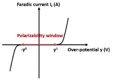
1.3.3. Polarizable Interface and Polarizability Window
Figure 1.10: Schemes of two behaviors of the interface ideally non-polarizable (left) and polarizable (right), image taken from [77].
When two electrodes are placed in a liquid electrolyte and applied by a potential difference, two behaviors exist: either the charge transfer takes place immediately at the solid-liquid interface and the electrons can be transferred from one electrode to the other by the ionic carriers of liquid; or the charge transfer does not take place at the interface but instead by the accumulation of charges at the solid-liquid interface. The former is called ideally non-polarizable interface (see left image of Figure 1.10 [77]), resulting in immediately electrochemical reaction and faradic current, while the latter is called ideally polarizable interface (see right image of Figure 1.10 [77]), resulting in purely capacitive behavior and no charges transfer, in other word, no faradic current.
Figure 1.11: The faradic current curve under function of over-potential for a symmetric interface.
The window of polarizability is a limited range of over-potential γ where the faradic current cannot be observed with a weak linear dependence [77]. In a case of symmetric interface, this faradic current can be described as Formula 1-19 [77]:
17
𝐼𝐹 = 𝐼0sinh( 𝛾
𝛾0) (1-19)
where I0 is the typical surface current, γ0 is the energy barrier potential. The polarizability window is
the area that γ varies within γ0, as shown in Figure 1.11. However, in reality, this window is rarely
symmetric due to the electrochemical reactions, such as the reduction and the oxidation. Moreover, changes in liquid electrolyte will also influence on the polarizability window, like adding another electrolyte or diluting the electrolyte.
1.4. Conclusions
This chapter gives an overview of the thesis background, from the basic of the CE to the birth of the µFWB that has improved CE technology. During the last ten years, the µFWB configuration has been developed and improved to better adapt to hydrodynamics and electrodes implantation. In my thesis work, I used the 3rd generation of this device that will be explained and detailed in Chapter 3. And I
mainly concentrated my work about the adhesion ability of the polarizable interface (a CNx film that was few studied in the world) on two major sticking underlayers (SiC and Pt) for three different PI-FFET configurations, as well as some microfluidic experiments to study PI-FFET.
R
EFERENCES:
[1] Q. Zhang, M. Zhang, L. Djeghlaf, J. Bataille, J. Gamby, A-M. Haghiri-Gosnet, and A. Pallandre, “Logic digital fluidic in miniaturized functional devices: Perspective to the next generation of microfluidic lab-on-chips,” Electrophoresis, vol. 38, pp. 953-976, 2017.
[2] G. M. Whitesides, “The origins and the future of microfluidics,” Nature, vol. 442, pp. 368-373, 2006.
[3] N-T. Nguyen, M. Hejazian, C. H. Ooi, and N. Kashaninejad, “Recent advances and future perspectives on microfluidic liquid handling,” Micromachines, vol. 8, pp. 186-206, 2017. [4] N-T. Nguyen and S. T. Wereley, “Fundamentals and applications of microfluidics,” Artech
House, London, UK, 2002.
[5] N-T. Nguyen, S. A. M. Shaegh, N. Kashaninejad, and D-T. Phan, “Design, fabrication and characterization of drug delivery systems based on lab-on-a-chip technology,” Adv. Drug Deliv.
Rev., vol. 65, pp. 1403-1419, 2013.
[6] D. R. Reyes, D. Iossifidis, P-A. Auroux, and A. Manz, “Micro total analysis systems. 1. Introduction, theory, and technology,” Anal. Chem., vol. 74, pp. 2623-2636, 2002.
[7] W. Jung, J. Han, J-W. Choi, and C. H. Ahn, “Point-of-care testing (POCT) diagnostic systems using microfluidic lab-on-a-chip technologies,” Microelectron. Eng., vol. 132, pp. 46-57, 2015. [8] M. Sonker, V. Sahore, and A. T. Woolley, “Recent advances in microfluidic sample preparation
and separation techniques for molecular biomarker analysis: A critical review,” Anal. Chim.
18
[9] K. K. R. Tetala and M. A. Vijayalakshmi, “A review on recent developments for biomolecule separation at analytical scale using microfluidics devices,” Anal. Chim. Acta, vol. 906, pp. 7-21, 2016.
[10] J. V. Pagaduan, V. Sahore, and A. T. Woolley, “Applications of microfluidics and microchip electrophoresis for potential clinical biomarker analysis,” Anal. Bioanal. Chem., vol. 407, pp. 6911-6922, 2015.
[11] S. M. Shameli and C. L. Ren, “Microfluidic two-dimensional separation of proteins combining temperature gradient focusing and sodium dodecyl sulfate-polyacrylamide gel electrophoresis,” Anal. Chem., vol. 87, pp. 3593-3597, 2015.
[12] R. Wu, Y. P. Seah, and Z. Wang, “Microfluidic chip for stacking, separation and extraction of multiple DNA fragments,” J. Chromatogr. A, vol. 1437, pp. 219-225, 2016.
[13] E. A. Redman, N. G. Batz, J. S. Mellors, and J. M. Ramsey, “Integrated microfluidic capillary electrophoresis-electrospray ionization devices with online MS detection for the separation and characterization of intact monoclonal antibody variants,” Anal. Chem., vol. 87, pp. 2264-2272, 2015.
[14] P. Batalla, A. Martin, M. A. Lopez, M. C. Gonzalez, and A. Escarpa, “Enzyme-based microfluidic chip coupled to graphene electrodes for the detection of d-amino acid enantiomer-biomarkers,” Anal. Chem., vol. 87, pp. 5074-5078, 2015.
[15] J. V. Pagaduan, M. Ramsden, K. O’Neill, and A. T. Woolley, “Microchip immunoaffinity electrophoresis of antibody-thymidine kinase 1 complex,” Electrophoresis, vol. 36, pp. 813-817, 2015.
[16] V. Sahore, S. Kumar, C. I. Rogers, J. K. Jensen, M. Sonker, and A. T. Woolley, “Pressure-actuated microfluidic devices for electrophoretic separation of pre-term birth biomarkers,” Anal.
Bioanal. Chem., vol. 408, pp. 599-607, 2016.
[17] F. Lin, S. Yu, L. Gu, X. Zhu, J. Wang, H. Zhu, Y. Lu, Y. Wang, Y. Deng, and L. Geng, “In situ photo-immobilized pH gradient isoelectric focusing and zone electrophoresis integrated two-dimensional microfluidic chip electrophoresis for protein separation,” Microchim. Acta, vol. 182, pp. 2321-2328, 2015.
[18] A. J. Laki, “Microfluidic particle separation techniques for biomedical use,” PhD thesis, Pazmany Peter Catholic University, 2015.
[19] J. Shi, S. Yazdi, S-C. S. Lin, X. Ding, I-K. Chiang, K. Sharp, and T. J. Huang, “Three-dimensional continuous particle focusing in a microfluidic channel via standing surface acoustic waves (SSAW),” Lab Chip, vol. 11, pp. 2319-2324, 2011.
[20] J. Shi, H. Huang, Z. Stratton, Y. Huang, and T. J. Huang, “Continuous particle separation in a microfluidic channel via standing surface acoustic waves (SSAW),” Lab Chip, vol. 9, pp. 3354-3359, 2009.
19
[21] J. Nam, H. Lim, D. Kim, and S. Shin, “Separation of platelets from whole blood using standing surface acoustic waves in a microchannel,” Lab Chip, vol. 11, pp. 3361-3364, 2011.
[22] T. Laurell, F. Petersson, and A. Nilsson, “Chip integrated strategies for acoustic separation and manipulation of cells and particles,” Chem. Soc. Rev., vol. 36, pp. 492-506, 2007.
[23] J. Shi, X. Mao, D. Ahmed, A. Colletti, and T. J. Huang, “Focusing microparticles in a microfluidic channel with standing surface acoustic waves (SSAW),” Lab Chip, vol. 8, pp. 221-223, 2008. [24] T. Franke, S. Braunmuller, L. Schmid, A. Wixforth, and D. A. Weitz, “Surface acoustic wave
actuated cell sorting (SAWACS),” Lab Chip, vol. 10, pp. 789-794, 2010.
[25] Y. Li, C. Dalton, H. J. Crabtree, G. Nilsson, and K. V. I. S. Kaler, “Continuous dielectrophoretic cell separation microfluidic device,” Lab Chip, vol. 7, pp. 239-248, 2007.
[26] A. Valero, T. Braschler, A. Rauch, N. Demierre, Y. Barral, and P. Renaud, “Tracking and synchronization of the yeast cell cycle using dielectrophoretic opacity,” Lab Chip, vol. 11, pp. 1754-1760, 2011.
[27] M. J. Hilhorst, G. W. Somsen, and G. J. de Jong, “Capillary electrokinetic separation techniques for profiling of drugs and related products,” Electrophoresis, vol. 22, pp. 2542-2564, 2001. [28] H-H. Cui, J. Voldman, X-F. He, and K-M. Lim, “Separation of particles by pulsed
dielectrophoresis,” Lab Chip, vol. 9, pp. 2306-2312, 2009.
[29] S-I. Han, S-M. Lee, Y-D. Joo, and K-H. Han, “Lateral dielectrophoretic microseparators to measure the size distribution of blood cells,” Lab Chip, vol. 11, pp. 3864-3872, 2011.
[30] M. D. Vahey and J. Voldman, “Emergent behavior in particle-laden microfluidic systems informs strategies for improving cell and particle separations,” Lab Chip, vol. 11, pp. 2071-2080, 2011.
[31] L. Wang, L. A. Flanagan, N. L. Jeon, E. Monuki, and A. P. Lee, “Dielectrophoresis switching with vertical sidewall electrodes for microfluidic flow cytometry,” Lab Chip, vol. 7, pp. 1114-1120, 2007.
[32] H-S. Moon, K. Kwon, S-I. Kim, H. Han, J. Sohn, S. Lee, and H-I. Jung, “Continuous separation of breast cancer cells from blood samples using multi-orifice flow fractionation (MOFF) and dielectrophoresis (DEP),” Lab Chip, vol. 11, pp. 1118-1125, 2011.
[33] H. Lee, J. Jung, S-I. Han, and K-H. Han, “High-speed RNA microextraction technology using magnetic oligo-dT beads and lateral magnetophoresis,” Lab Chip, vol. 10, pp. 2764-2770, 2010. [34] F. Shen, H. Hwang, Y. K. Hahn, and J-K. Park, “Label-free cell separation using a tunable
magnetophoretic repulsion force,” Anal. Chem., vol. 84, pp. 3075-3081, 2012.
[35] T. Zhu, R. Cheng, S. A. Lee, E. Rajaraman, M. A. Eiteman, T. D. Querec, E. R. Unger, and L. Mao, “Continuous-flow ferrohydrodynamic sorting of particles and cells in microfluidic devices,”
20
[36] A. I. Rodriguez-Villarreal, M. D. Tarn, L. A. Madden, J. B. Lutz, J. Greenman, J. Samitier, and N. Pamme, “Flow focusing of particles and cells based on their intrinsic properties using a simple diamagnetic repulsion setup,” Lab Chip, vol. 11, pp. 1240-1248, 2011.
[37] D. Robert, N. Pamme, H. Conjeaud, F. Gazeau, A. Iles, and C. Wilhelm, “Cell sorting by endocytotic capacity in a microfluidic magnetophoresis device,” Lab Chip, vol. 11, pp. 1902-1910, 2011.
[38] N. Pamme and C. Wilhelm, “Continuous sorting of magnetic cells via on-chip free-flow magnetophoresis,” Lab Chip, vol. 6, pp. 974-980, 2006.
[39] P. Bhardwaj, P. Bagdi, and A. K. Sen, “Microfluidic device based on a microhydrocyclone for particle-liquid separation,” Lab Chip, vol. 11, pp. 4012-4021, 2011.
[40] D. Huh, J. H. Bahng, Y. Ling, H-H. Wei, O. D. Kripfgans, J. B. Fowlkes, J. B. Grotberg, and S. Takayama, “Gravity-driven microfluidic particle sorting device with hydrodynamic separation amplification,” Anal. Chem., vol. 79, pp. 1369-1376, 2007.
[41] R. Gorkin, J. Park, J. Siegrist, M. Amasia, B. S. Lee, J-M. Park, J. Kim, H. Kim, M. Madou, and Y-K. Cho, “Centrifugal microfluidics for biomedical applications,” Lab Chip, vol. 10, pp. 1758-1773, 2010.
[42] S. Haeberle, T. Brenner, R. Zengerle, and J. Ducree, “Centrifugal extraction of plasma from whole blood on a rotating disk,” Lab Chip, vol. 6, pp. 776-781, 2006.
[43] H. Zhang, E. Tu, N. D. Hagen, C. A. Schnabel, M. J. Paliotti, W. S. Hoo, P. M. Nguyen, J. R. Kohrumel, W. F. Butler, M. Chachisvillis, and P. J. Marchand, “Time-of-flight optophoresis analysis of live whole cells in microfluidic channels,” Biomed. Microdevices, vol. 6, pp. 11-21, 2004.
[44] B. S. Zhao, Y-M. Koo, and D. S. Chung, “Separations based on the mechanical forces of light,”
Anal. Chim. Acta, vol. 556, pp. 97-103, 2006.
[45] T-H. Wu, Y. Chen, S-Y. Park, J. Hong, T. Teslaa, J. F. Zhong, D. D. Carlo, M. A. Teitell, and P-Y. Chiou, “Pulsed laser triggered high speed microfluidic fluorescence activated cell sorter,” Lab
Chip, vol. 12, pp. 1378-1383, 2012.
[46] F. F. Reuss, “Sur un nouvel effet de l’électricité galvanique,” Mémoires de la Société Impériale des Naturalistes de Moscou, vol. 2, pp. 327-337, 1809.
[47] A. Tiselius, “A new apparatus for electrophoretic analysis of colloidal mixtures,” Trans. Faraday
Soc., vol. 33, pp. 524-531, 1937.
[48] D. Janasek, J. Franzke, and A. Manz, “Scaling and the design of miniaturized chemical-analysis systems,” Nature, vol. 442, pp. 374-380, 2006.
[49] H. Bruus, “Theoretical microfluidics,” Oxford University Press, Oxford, UK, 2008. [50] “Ion-Dipole Forces,” https://www.chem.purdue.edu/gchelp/liquids/iondip.html.
21
[51] M. X. Zhou and J. P. Foley, “Quantitative theory of electroosmotic flow in fused-silica capillaries using an extended site-dissociation-site-binding model,” Anal. Chem., vol. 78, pp. 1849-1858, 2006.
[52] D. R. Baker, “Capillary electrophoresis,” Wiley-Interscience, New York, USA, 1995.
[53] O. Z. Stern, “Theory of the electrical double layer,” Electrochem, vol. 30, pp. 508-516, 1924. [54] H. L. F. von Helmholtz, “Ueber einige Gesetze der Vertheilung elektrischer Ströme in
körperlichen Leitern mit Anwendung auf die thierisch-elektrischen Versuche,” Annalen der
Physik, vol. 165, pp. 211-233, 1853.
[55] L. G. Gouy, “Sur la constitution de la charge électrique à la surface d’un électrolyte,” J. Phys.
Theor. Appl., vol. 9, pp. 457-468, 1910.
[56] D. L. Chapman, “A contribution to the theory of electrocapillarity,” Philos. Mag., vol. 25, pp. 475-481, 1913.
[57] M. Smoluchowski, “Elektrische endosmose und strömungsströme,” Handbuch der Elektrizität und des Magnetismus, vol. 2, pp. 366-428, B. GRAETZ, Leipzig, 1914.
[58] C. Gerthsen, H. O. Kneser, and H. Vogel, “Physik,” 16th Edition, Springer Berlin, Germany, 1989.
[59] A. Manz, C. S. S. Effenhauser, N. Burggraf, D. J. Harrison, K. Seiler, and K. Fluri, “Electroosmotic pumping and electrophoretic separations for miniaturized chemical analysis systems,” J.
Micromech. Microeng., vol. 4, pp. 257-265, 1994.
[60] A. Sze, D. Erickson, L. Ren, and D. Li, “Zeta-potential measurement using the Smoluchowski equation and the slope of the current-time relationship in electroosmotic flow,” J. Colloid
Interface Sci., vol. 261, pp. 402-410, 2003.
[61] E. K. Zholkovskij, A. E. Yaroshchuk, J. H. Masliyah, and J. D. Ribas, “Broadening of neutral solute band in electroosmotic flow through submicron channel with longitudinal non-uniformity of zeta potential,” Colloids Surf. A, vol. 354, pp. 338-346, 2010.
[62] E. K. Zholkovskij and J. H. Masliyah, “Influence of cross-section geometry on band broadening in plug-flow microchannels,” Chem. Eng. Sci., vol. 61, pp. 4155-4164, 2006.
[63] A. Pallandre, “Intégration du transistor fluidique à effet de champs et à interface polarisable dans un pont de Wheatstone,” HDR, Université Paris-Sud, 2015.
[64] A. Plecis, J. Tazid, A. Pallandre, P. Martinhon, C. Deslouis, Y. Chen, and A-M. Haghiri-Gosnet, “Flow field effect transistors with polarizable interface for EOF tunable microfluidic separation devices,” Lab Chip, vol. 10, pp. 1245-1253, 2010.
[65] L. Baur, C. S. van de Griend, and H. Wätzig, “Electroosmotic flow variations caused by the volatility of buffer components: diagnosis and therapy,” J. Chromatogr. A, vol. 979, pp. 97-103, 2002.
22
[66] W. Schüetzner and E. Kenndler, “Electrophoresis in synthetic organic polymer capillaries: variation of electroosmotic velocity and zeta potential with pH and solvent composition,” Anal.
Chem., vol. 64, pp. 1991-1995, 1992.
[67] M. A. Hayes, I. Kheterpal, and A. G. Ewing, “Effects of buffer pH on electroosmotic flow control by an applied radial voltage for capillary zone electrophoresis,” Anal. Chem., vol. 65, pp. 27-31, 1993.
[68] B. J. Kirby and E. F. Hasselbrink Jr., “Zeta potential of microfluidic substrates: 1. Theory, experimental techniques, and effects on separations,” Electrophoresis, vol. 25, pp. 187-202, 2004.
[69] A. Varenne and S. Descroix, “Recent strategies to improve resolution in capillary electrophoresis: A review,” Anal. Chim. Acta, vol. 628, pp. 9-23, 2008.
[70] E. A. S. Doherty, R. J. Meagher, M. N. Albarghouthi, and A. E. Barron, “Microchannel wall coatings for protein separations by capillary and chip electrophoresis,” Electrophoresis, vol. 24, pp. 34-54, 2003.
[71] A. Pallandre, B. de Lambert, R. Attia, A. M. Jonas, and J-L. Viovy, “Surface treatment and characterization : perspectives to electrophoresis and lab-on-chips,” Electrophoresis, vol. 27, pp. 584-610, 2006.
[72] R. B. M. Schasfoort, S. Schlautmann, J. Hendrikse, and A. van den Berg, “Field-effect flow control for microfabricated fluidic networks,” Science, vol. 286, pp. 942-945, 1999.
[73] E. J. van der Wouden, T. Heuser, D. C. Hermes, R. E. Oosterbroek, J. G. E. Gardeniers, and A. van den Berg, “Field-effect control of electro-osmotic flow in microfluidic networks,” Colloids
Surf. A, vol. 267, pp. 110-116, 2005.
[74] A. J. Bard and L. R. Faulkner, “Electrochemical methods,” John Wiley & Sons, New York, USA, 1980.
[75] A. Plecis and Y. Chen, “Microfluidic analogy of the Wheatstone bridge for systematic investigations of electro-osmotic flows,” Anal. Chem., vol. 80, pp. 3736-3742, 2008.
[76] G. Desmet and G. V. Baron, “Chromatographic explanation for the side-wall induced band broadening in pressure-driven and shear-driven flows through channels with a high aspect-ratio rectangular cross-section,” J. Chromatogr. A, vol. 946, pp. 51-58, 2002.
[77] A. Plecis, “Etude et contrôle de la charge de surface dans les dispositifs micro/nanofluidiques : nouveaux outils pour les sciences séparatives,” PhD thesis, Université Paris-Sud, 2008.
23
Chapter 2: Simplification of EOF Measurement Equipment
2.1. Overview
In the early Section 1.3.1, we have presented the polarizable interface flow field effect transistor (PI-FFET) designed by our team (Figure 1.7A). An ideal polarizable interface fluidic transistor should have no electrochemical reactions, such as electronic transfer or faradic current from solid to the electrolyte, which is normally caused by reduction or oxidation of chemical substance at the electrode [1, 2]. As we have already known that the over-potential γ is a potential difference between the electrolyte potential φ and the control gate voltage V (see details in Section 1.3.1). As long as it remains within a potential window |γ|<γ0, the faradic current could be negligible [3]. The factor γ0 is called the faradic
over-potential, depending on the conduction layer-electrolyte couple [4]. Therefore, to avoid such electrochemical reactions, we have integrated two electrolyte measuring electrodes, i.e. reference electrodes near to the entrance and the exit of the central channel, aiming to precisely measure the electrolyte potential φ at both ends of the fluidic transistor in order to accurately apply the control gate voltage V on the two PI-FFET control electrodes, i.e. gate electrodes, thus making sure that |V-φ| = |γ|<γ0, as illustrated in Figure 2.1 [5].
Figure 2.1: The simplified electronic configuration of the PI-FFET, image taken from [5].
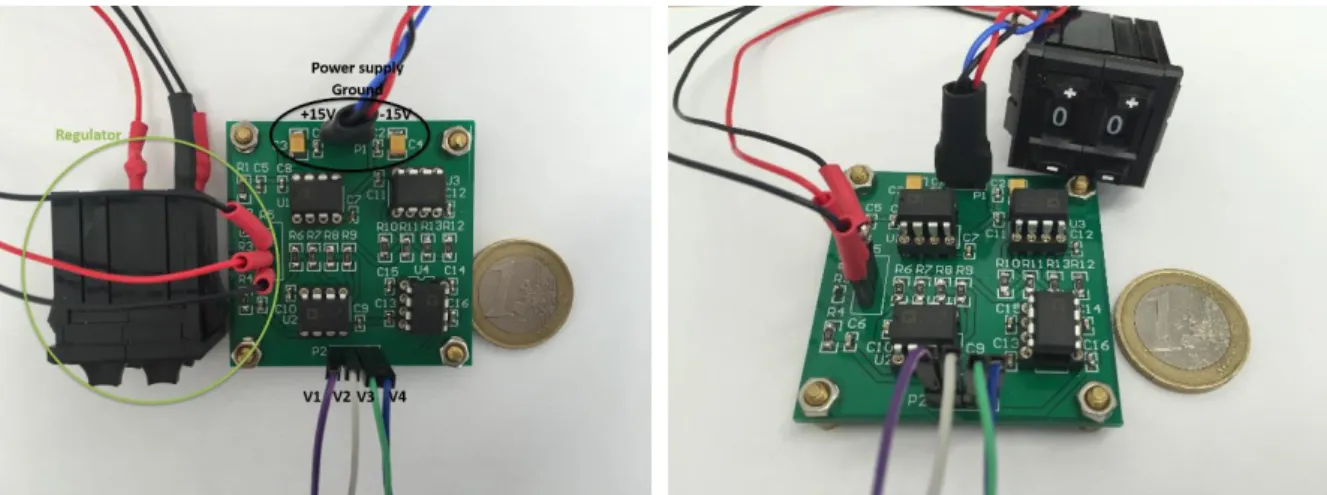
The outermost pair of electrodes provides the transverse electrophoretic field. Two voltage followers circled in yellow were two big equipments in the past, as shown in Figure 3.8 of Section 3.3.1. In this chapter, we will present a small portable printed circuit board (PCB) that replaces these two big heavy boxes.
24
2.2. Theoretical Analysis
Figure 2.2: The electronic conception of the voltage follower (above) and its electronic model (below).
The conception of the voltage follower is shown in the image above of Figure 2.2. The electrophoretic field is applied by a +15V/ground source meter unit or power supply unit with low current. V1 and V4 represent the voltage of the electrolyte that the two followers read about, while V2 and V3 represent the voltage employed on the gate electrodes according to V1 and V4 respectively. The difference between V1 and V2 or V4 and V3 should remain within the potential window, which is from -3.5V to +3.5V of this device [6]. To be on the safe side, ΔV is chosen within -1V/+1V. Such voltage follower is very simple in electronic model, as shown in image below of Figure 2.2: four voltage followers without gain, two adders, and one regulator. In the following part, we will introduce design of each part.
2.2.1. Adder