HAL Id: tel-03140181
https://tel.archives-ouvertes.fr/tel-03140181v2
Submitted on 22 Apr 2021HAL is a multi-disciplinary open access archive for the deposit and dissemination of sci-entific research documents, whether they are pub-lished or not. The documents may come from teaching and research institutions in France or abroad, or from public or private research centers.
L’archive ouverte pluridisciplinaire HAL, est destinée au dépôt et à la diffusion de documents scientifiques de niveau recherche, publiés ou non, émanant des établissements d’enseignement et de recherche français ou étrangers, des laboratoires publics ou privés.
Disorder-induced localization effects in nitride
semiconductor compounds and devices
Wiebke Hahn
To cite this version:
Wiebke Hahn. Disorder-induced localization effects in nitride semiconductor compounds and devices. Materials Science [cond-mat.mtrl-sci]. Institut Polytechnique de Paris, 2020. English. �NNT : 2020IP-PAX049�. �tel-03140181v2�
Disorder-induced localization
effects in nitride semiconductor
compounds and devices
Thèse de doctorat de l’Institut Polytechnique de Paris
préparée à École Polytechnique
École doctorale n°626 École Doctorale
de l’Institut Polytechnique de Paris (ED IP Paris)
Spécialité de doctorat : Physique
Thèse présentée et soutenue à Palaiseau de soutenance, le 17/09/2020, par
Wiebke Hahn
Composition du Jury : Nicolas Grandjean
Professeur
École Polytechnique Fédérale de Lausanne – LASPE, Suisse Rapporteur
Philippe Dumas
Professeur, Aix-Marseille Université – CINaM, France Rapporteur
James S. Speck
Professeur
UCSB – Materials Department, États-Unis Examinateur
Sir Richard Friend
Professeur
University of Cambridge – Cavendish Laboratory, Royaume-Uni Examinateur
Silke Biermann
Professeur
École Polytechnique – CPHT, France Présidente
Mathieu Kociak
Directeur de Recherche
Université Paris Sud – LPS, France Examinateur
Jacques Peretti
Directeur de Recherche
École Polytechnique – LPMC, France Directeur de thèse
Claude Weisbuch
Professeur
École Polytechnique – LPMC, France
UCSB – Materials Department, États-Unis Co-encadrant
NNT
:
20
20
IP
PA
X
04
9
Acknowledgements
I strongly believe that true progress can only be achieved when people with different expertise come together to work for the best outcome possible. I was lucky to pursue my PhD thesis in such an environment. Therefore, I thank Mathis Plapp for welcoming me as a PhD student in the Laboratoire de Physique de la Matière Condensée at École Polytechnique.
I would like to express my deep gratitude to my supervisors and my mentor: Jacques Peretti, Yves Lassailly, and Claude Weisbuch. Jacques gave me the freedom to work and develop this scientific project. At the same time, he encouraged me enthusiastically with his useful critiques and comments. Yves taught me valuable lessons on the experimental study of semiconductors and offered me generous support far beyond the usual. Claude is a real mentor. He has shaped my scientific way of thinking and problem-solving. He also introduced me to the scientific community and let me build important connections. The discussions with Jacques, Yves, and Claude have always been illuminating, inspiring, and most of all motivating. I thank them for their generous support, guidance, and persistent help. I will always be in their intellectual debt.
As every PhD student from the Laboratoire de Physique de la Matière Condensée (LPMC), I am particularly grateful for the tremendous assistance given by Lucio Martinelli. Lucio always took the time to answer all of my questions from UHV leak detection and building a new optical setup to “where can I buy Pecorino Romano in Paris?”.
I would like to extend my sincere thanks to the whole “Electrons-Photons-Surfaces” group of LPMC. Especially, I would like to thank Fausto Sirotti and Alistair Rowe for the help with the UHV chamber as well as the development of the STL setup.
Many thanks to the Irregularity group of LPMC, in particular to Marcel Filoche and Jean-Marie Lentali, for the theoretical modeling and calculations, but also to Abel Thayil, Pierre Pelletier and Jean-Philippe Banon, for the fruitful discussions.
It has been a great pleasure to work with Mylène Sauty. We make quite a team! I especially thank her for all her questions and her strong motivation. I am sure she will achieve great things with the STL experiment.
I would also like to express my gratitude to the help of Fouad Maroun. He has been a great support in implementing the homemade adaptions to the Omicron STM, coding in LabVIEW, and taking the SEM measurements.
Thanks should also go to André Wack for the fabrication of mechanical components, to Didier Lenoir for building the electronic circuits for the STM, and to Sandrine Tusseau-Nenez for the HRXRD measurements.
From the moment I set foot at LPMC, I always felt welcome due to the friendly and at the same time inspiring atmosphere between all the members of the laboratory. It has been a real pleasure to be part of this laboratory.
Acknowledgements
I would also like to acknowledge the financial support of the French National Research Agency (ANR)1, the Labex Nano-Saclay2 as well as the Simons foundation3. Many thanks go to our
(international) collaborators, in particular, at the University of California in Santa Barbara, for the growth of the samples, as well as at the Institut des Sciences Moléculaires d'Orsay, for inviting me to conduct experiments in their laboratory.
Thanks to Aurélien David for fruitful discussions and the samples grown at Soraa Inc.
I would also like to thank the “Freundestorus” back in Germany. Without them, studying physics would have been much harder and less fun.
I cannot begin to express my gratitude to my family who always encourages and supports me without doubt. Without them this journey would not have been possible.
Finally, I would like to thank Valerio Peri. I am deeply grateful for all of his support throughout the ups and downs of the rollercoaster of emotions of this research project as well as all his valuable comments and suggestions on this manuscript. Thank you very much for everything. You are my safe harbor!
1 This work was supported by the French National Research Agency (ANR): CRIPRONI and ELENID projects,
grants No. ANR-14-CE05-0048-01 and ANR-17-CE24-0040-01.
2 This work was supported by the ELIDE project, a public grant overseen by the French National Research
Agency (ANR) as part of the “Investissements d’Avenir” program: Labex NanoSaclay, reference ANR-10-LABX-0035.
Content
Acknowledgements _______________________________________________________________________________________ v Content __________________________________________________________________________________________________ vii List of acronyms _________________________________________________________________________________________ ix Introduction _____________________________________________________________________________________________ 11 1 III-nitride semiconductors _______________________________________________________________________ 15 1.1 III-nitride semiconductors __________________________________________________________ 15 1.2 Challenges of III-nitride semiconductors __________________________________________ 16 1.2.1.1 Growth of III-nitride semiconductors ______________________________________________ 16 1.2.1.2 Conductivity of p-doped GaN _______________________________________________________ 17 1.2.1.3 Polarization effects __________________________________________________________________ 17 1.2.1.4 Carrier recombination in III-nitride ________________________________________________ 17 1.2.1.5 Green gap _____________________________________________________________________________ 18 1.3 Compositional disorder in nitride alloys___________________________________________ 19 1.4 Disorder-induced localization effects ______________________________________________ 20 1.5 Experimental evidence of disorder-induced localization effects ________________ 21 2 Experimental method _____________________________________________________________________________ 25 2.1 Techniques ___________________________________________________________________________ 25 2.1.1 Scanning tunneling microscopy ____________________________________________________ 25 2.1.2 Scanning tunneling electroluminescence __________________________________________ 27 2.2 Experimental setups _________________________________________________________________ 27 2.2.1 STL in ambient atmosphere _________________________________________________________ 27 2.2.2 STL in ultra-high vacuum ___________________________________________________________ 30 2.3 Experimental procedure ____________________________________________________________ 34 2.3.1 STM tips ______________________________________________________________________________ 34 2.3.2 Taking an STL measurement _______________________________________________________ 35 3 Results _____________________________________________________________________________________________ 37 3.1 Samples _______________________________________________________________________________ 37 3.1.1 Sample structure _____________________________________________________________________ 37 3.1.2 Sample preparation _________________________________________________________________ 38 3.1.2.1 Cleaning ______________________________________________________________________________ 38 3.1.2.2 Contacts ______________________________________________________________________________ 38 3.1.3 Sample characterization ____________________________________________________________ 39 3.2 Scanning tunneling electroluminescence spectroscopy __________________________ 41Content
3.2.1 Electroluminescence tunneling injection spectroscopy __________________________ 41 3.2.2 Electroluminescence spectroscopy under local tunneling electron injection ___ 42 3.2.3 Line scans ____________________________________________________________________________ 44 3.2.4 Comparison of STL measurements with LL theory simulations _________________ 47 3.3 Analysis of STL spectra line shape _________________________________________________ 48 3.3.1 Analysis of line scans at low tunneling current (2 nA)____________________________ 49 3.3.2 Analysis of line scans at high tunneling current (20 nA) _________________________ 53 3.4 A model accounting for energy relaxation and transport ________________________ 55 3.5 Dependence of the local STL spectrum on tunneling parameters _______________ 57 3.6 Further investigations on single localized state emission ________________________ 60 3.7 Conclusion and discussion __________________________________________________________ 65 4 Preliminary results on future research directions _____________________________________________ 67 4.1 DQW structures for the study of perpendicular transport and STL resolution _ 67 4.2 Low temperature STL measurements______________________________________________ 69 4.3 Localization effects in nitride heterostructures of industrial standard _________ 72 4.3.1 Sample structure and characterization ____________________________________________ 72 4.3.2 STL spectroscopy ____________________________________________________________________ 75 4.4 STL on n-type nitride heterostructures: localization of holes ____________________ 78 5 Conclusion and perspectives _____________________________________________________________________ 83 A. Procedure for STL data analysis _________________________________________________________________ 87 A.1 Data treatment of STL spectra _________________________________________________________ 87 A.1.1 Elimination of artefacts _________________________________________________________________ 88 A.1.2 Background correction _________________________________________________________________ 88 A.1.3 Smoothing procedure___________________________________________________________________ 89 A.1.4 Spectra analysis _________________________________________________________________________ 89 A.2 Pearson correlation _____________________________________________________________________ 90 B. Comparison between our STL setups ____________________________________________________________ 91 C. HRXRD measurements ____________________________________________________________________________ 93 Bibliography ____________________________________________________________________________________________ 95
List of acronyms
1D DDCC One-Dimensional Drift-Diffusion Charge Control
AFM Atomic force microscopy
BBR Band bending region
BEEM Ballistic electron emission spectroscopy
CL Cathodoluminescence
CR Cosmic ray
DQW Double quantum well
EELS Electron energy loss spectroscopy
EMCCD Electron-multiplying charge-coupled device EQE External quantum efficiency
FWHM Full width at half maximum HRXRD High resolved X-ray diffraction HVPE Hydride vapor phase epitaxy HWHM Half width at half maximum
Int. Intensity
IQE Internal quantum efficiency
ITO Indium tin oxide
IV Current-Voltage (characteristics)
LED Light emitting diode
LL Localization landscape theory
MBE Molecular beam epitaxy
MOCVD Metalorganic chemical vapor deposition
PL Photoluminescence
QCSE Quantum confined Stark effect
QW Quantum well
RT Room temperature
SEM Scanning electron microscopy
SQW Single quantum well
STEM Scanning transmission electron microscopy STL Scanning tunneling electroluminescence
STM Scanning tunneling microscopy
STS Scanning tunneling spectroscopy
UHV Ultra-high vacuum
UID Unintentionally doped
Introduction
English version
This PhD thesis deals with disorder-induced localization effects in nitride semiconductor compounds and devices by the experimental approach of scanning tunneling electroluminescence (STL) spectroscopy.
Throughout history lighting has played a crucial role in the development of humankind. Ever since, we have been looking for more efficient ways to produce light. Our means to produce light evolved from flames of burning materials such as in candles, oil lamps, kerosene and gas lamps, to resistive heating of filaments and Thomas Edison’s incandescent light bulb [1], to the electron discharge in fluorescent lamps and finally to efficient solid-state lighting in light-emitting diodes (LEDs).
Nitride semiconductor compounds such as GaN, InN, AlN and their alloys are nowadays ubiquitous in optoelectronic devices, e.g., LEDs and lasers devices and power technologies. Their ultimately successful story begins more than hundred years ago. Their development required a slow but steady progress. Prominently, the discovery of solid-state light (SSL) emitters, the development of p-n junctions and their application to lighting, as well as the advancement in heterostructure fabrication played an essential role. The first LEDs based on SiC exhibited only a limited quantum efficiency of 2 × 10⁻⁹ , even in pure materials [2]. This low performance triggered a subsequent vast search for materials better suited for solid-state lighting. Although nitrides were already considered in the 60s and early 70s [3,4], they were subsequently neglected due to their many difficulties. These drawbacks, such as the lack of a native substrate, the poor growth quality of the material, the difficulty to p-dope GaN or its alloys were mainly overcome by the pioneering work of Isamu Akasaki, Hiroshi Amano and Shuji Nakamura. Their achievements finally led to efficient blue nitride-based LEDs and were awarded with the Nobel Prize in Physics in 2014 [5]. A complete review on the historical developments of LEDs and their challenges is provided by C. Weisbuch in [6–8].
The wide usage of the efficient nitride-based LEDs has a major impact on the energy consumption due to lighting. However, only with LEDs working at their physical limit energy savings of over 75% of the total energy consumption due to lighting can be achieved [9]. To push LEDs to their efficiency limit, further challenges of the III-nitride based semiconductors have to be overcome. The goal of this PhD thesis is to foster our understanding of fundamental material properties of nitride ternary alloys. In particular, the objective of this thesis is to address the problem of localization effects induced by alloy disorder. The active region of opto-electronic devices commonly incorporates ternary alloys which exhibit intrinsic composition disorder due to the random positioning of atoms on the crystal lattice. In nitrides, the bandgap energy varies dramatically with alloy composition and spans over the whole spectral range from near IR to near UV. Therefore, the local intrinsic fluctuations of the alloy composition result in large potential fluctuations at the scale of a few nanometers which are thus expected to induce strong carrier localization effects that should impact the electronic processes. We have studied the localization effects due to alloy disorder in InGaN/GaN quantum wells at the relevant scale by an original local probe technique. The manuscript presented is structured as follows:
Introduction
• Chapter 1 – III-nitride semiconductors:
We introduce the challenges currently faced in III-nitride semiconductor compounds and devices related to the extrinsic to intrinsic material properties and their theoretical modeling.
• Chapter 2 – Experimental method:
We describe the scanning tunneling electroluminescence (STL) setups and the experimental procedures that we developed to study disorder-induced localization effects in nitride ternary alloys.
• Chapter 3 – Results:
We show the capabilities of our experimental approach to probe electronic processes at the nanometer scale in heterostructures containing a single InGaN/GaN quantum well and evaluate the effect of the intrinsic ternary alloy disorder on the carrier dynamics. We further compare our experimental findings to the predictions of the localization landscape theory.
• Chapter 4 – Preliminary results on future research directions:
We present preliminary results on the investigation of several issues related to the disorder-induced localization effects: perpendicular transport in double quantum well structures, the temperature dependence of the local tunneling electroluminescence spectrum, a comparison of the local tunneling electroluminescence properties of samples produced in academic and industrial facilities, and the investigation of hole localization by STL in n-type InGaN/GaN structures.
• Chapter 5 – Conclusion and perspectives:
Finally, we conclude this thesis by highlighting the main results and give some perspectives to further investigate the effects of alloy disorder on the electronic processes in nitride heterostructures and devices by STL. Moreover, we discuss the application of our experimental approach to study localization effects in other materials and show the latest developments of our setup.
Introduction
Version française
L’objectif de cette thèse est la mise en évidence des effets de localisation induits par le désordre d’alliage dans les composés et dispositifs en nitrures semi-conducteurs par une approche expérimentale originale basée sur la microscopie d'électroluminescence à effet tunnel, dite STL. Tout au long de l'histoire, l'éclairage a joué un rôle crucial dans l’évolution économique et sociale de l'humanité. La production de lumière a évolué de la combustion de matériaux comme la bougie, l’huile, le kérosène et le gaz, au chauffage de filaments résistifs comme dans l'ampoule à incandescence de Thomas Edison [1], à la fluorescence des gaz dans les lampes à décharge et enfin à l'électroluminescence dans les diodes semi-conductrices.
Les composés semi-conducteurs à base de nitrure, tels que le GaN, l'InN, l'AlN et leurs alliages, sont aujourd'hui largement utilisés dans les diodes électroluminescentes (LED), les lasers et l'électronique de puissance. Leur histoire à succès commence il y a plus de cent ans. Leur développement est le résultat d’un long processus de recherche fondamentale. La découverte des émetteurs de lumière à l'état solide, le développement des diodes à jonctions p-n, ainsi que les progrès réalisés dans la fabrication des hétérostructures ont constitué des étapes clés dans ce développement. Les premières LED à base de SiC, émettant du côté des courtes longueurs d’onde du spectre visible, n'ont montré qu'une efficacité quantique limitée à 2 × 10⁻⁹, même dans des matériaux purs [2]. Cette performance modeste a suscité un vaste effort de recherche orienté vers des matériaux semi-conducteurs ayant de plus fortes efficacités quantiques. Bien que les nitrures aient été envisagés comme candidats potentiels dès les années 60 et au début des années 70 [3,4], ils ont par la suite été écartés en raison de nombreuses difficultés technologiques, telles que l'absence de substrat natif, la mauvaise qualité de croissance du GaN sur des substrats à fort désaccord de maille, la difficulté de réaliser un dopage de type p. C’est grâce aux travaux pionniers d’Isamu Akasaki, d’Hiroshi Amano et de Shuji Nakamura que la fabrication de LED à base de nitrure émettant efficacement dans le bleu a pu être développée. Cette découverte a été récompensée par le prix Nobel de physique en 2014 [5]. Une revue complète de l'historique du développement des LED et de leurs défis est présentée par C. Weisbuch dans [6–8].
L’utilisation de plus en plus large des LED à base de nitrure pour l'éclairage a un impact significatif sur la consommation d'énergie électrique. Cependant, pour réaliser les économies d'énergie attendues avec ces dispositifs, à savoir plus de 75 % de la consommation totale d'énergie due à l'éclairage [9], il est nécessaire de surmonter plusieurs difficultés liées aux propriétés intrinsèques des nitrures semi-conducteurs.
L'objectif de cette thèse de doctorat est la compréhension des propriétés électroniques fondamentales des alliages ternaires de nitrure et, plus particulièrement, des effets de localisation induits par le désordre d’alliage. En effets, la région active des dispositifs optoélectroniques incorpore généralement des alliages ternaires qui présentent un désordre de composition intrinsèque dû au positionnement aléatoire des atomes de l’alliage sur le réseau cristallin. Dans les nitrures, l’énergie de la bande interdite varie de façon abrupte avec la composition de l’alliage depuis le proche IR jusqu’au proche UV. Par conséquent, les fluctuations de composition dues au désordre intrinsèque d’alliage entraînent d'importantes fluctuations du potentiel électronique à l'échelle de quelques nanomètres qui induisent des effets de localisation des porteurs de charge. Au cours de ce travail, nous avons étudié les effets de localisation électronique dus au désordre d'alliage à l'échelle nanométrique dans les puits quantiques InGaN/GaN par une technique originale de microscopie à sonde locale qui permet d’accéder aux processus électroniques aux
Introduction
échelles pertinentes. Ce travail est décrit dans le présent manuscrit de thèse qui est structuré comme suit :
• Chapitre 1 - Les nitrures semi-conducteurs :
Nous introduisons les questions actuelles qui concernent les composés et dispositifs semi-conducteurs à base de nitrure, liées à leurs propriétés extrinsèques et intrinsèques ainsi qu’à leur modélisation théorique.
• Chapitre 2 - Méthodes expérimentales :
Nous décrivons les dispositifs expérimentaux de microscopie STL que nous avons développés pour étudier les effets de localisation induits par le désordre d’alliage dans les composés ternaires de nitrures.
• Chapitre 3 – Résultats :
Nous présentons les résultats de spectroscopie STL à l’échelle nanométrique obtenus sur des structures à puits quantiques InGaN/GaN et évaluons l'effet du désordre intrinsèque de l’alliage ternaire sur la dynamique des porteurs. Nous comparons ensuite nos résultats expérimentaux aux prédictions de la théorie du paysage de localisation.
• Chapitre 4 - Résultats préliminaires sur les futurs axes de recherche :
Nous présentons des résultats préliminaires sur plusieurs problématiques que nous avons abordées qui concernent l'étude du transport perpendiculaire dans les structures à double puits quantique, la dépendance en température de l’électroluminescence locale, la comparaison des propriétés d’électroluminescence locale d’échantillons produits dans des installations universitaires et industrielles, et l’étude de la localisation des trous dans les structures InGaN/GaN de type n.
• Chapitre 5 - Conclusion et perspectives :
Enfin, nous concluons cette thèse en mettant en évidence les principaux résultats obtenus et donnons des perspectives pour poursuivre l’étude, par la technique de microscopie STL, des processus électroniques à l’échelle du désordre d’alliage dans les nitrures. De plus, nous discutons de l'application de notre approche expérimentale à l'étude des effets de localisation dans d'autres matériaux et nous présentons les derniers développements de notre expérience.
1
III-nitride semiconductors
Although light-emitting diodes (LEDs) based on III-nitrides work already very efficiently and their applications led to significant energy savings, the nitride devices have to be pushed to their physical
limit to meet the full predicted impact of their usage. In the following, we point out the relevant material properties of III-nitride materials and the challenges faced by the nitride technology.
1.1
III-nitride semiconductors
III-nitride semiconductors such as GaN, InN, AlN and their alloys, e.g., InxGa1-xN or InxGayAl1−x−yN
exhibit unique material properties. Depending on their composition, their direct bandgap varies from about 0.7 eV corresponding to InN to 6.2 eV corresponding to AlN. The alloy bandgap thereby spans a wide wavelength range from the infrared over the visible spectrum to the deep ultraviolet (UV). Compared to other alloy compound semiconductors such as GaAs, which are grown in a zinc blend structure, cubic-like, III-nitride materials are commonly grown in wurtzite structure, hexagonal-like. The variation of bandgap of GaN, InN, AlN and their alloys as well as of other major semiconductors are shown in Figure 1.1 along with the corresponding wavelength.
Figure 1.1: Direct bandgap of GaN, InN, AlN and their alloys depending on composition, and other
major semiconductors and their alloys, against crystal lattice constant. Reprint from [6].
From Figure 1.1 the application of nitride semiconductor compounds in opto-electronics is a logic consequence. However, the route that led to the fabrication of an InGaN/GaN LED with high-brightness in 1994 [10] was long and required tremendous research efforts and breakthroughs which culminated in the recognition by the Nobel Prize in Physics in 2014.
The light emission efficiency of LEDs is expressed by their external quantum efficiency (EQE). The EQE is the product of the injection efficiency (injected current into the active region which are the quantum wells (QWs) of an LED), internal quantum efficiency (conversion efficiency of injected
1 III-nitride semiconductors
electron-hole pairs into photons inside the QWs), and the light extraction efficiency (ratio of photons emitted outside the LED to those generated inside) [7]. Multiplying the EQE by the
electrical efficiency (the ratio of the electrical energy, mainly affected by ohmic or contact losses
and quantum barrier heights in the active region, to the emitted photon energy), we obtain the
wall-plug efficiency (WPE).
Unfortunately, a high WPE does not suffice. From 1994 to 2012 LEDs covered only a minor role until they became cost effective enough to penetrate the market [8]. State of the art blue-emitting LEDs reach a WPE of above 70% at low current densities [11]. However, there is prospect of operating LEDs at WPE ≥ 100% due to thermoelectric pumping of carriers by lattice heat [12]. The increased usage of LEDs shows already significant impact on the total consumption of electricity due to lighting [13].
The optoelectronic applications of III-nitrides are not only limited to lighting with LEDs and laser diodes (LD). For example, UV-LEDs are used for disinfection and water purification [14] and nitride based vertical-cavity surface-emitting lasers are used for fiber optic communication. Besides these, nitride semiconductors also find wide-scale applications in power electronics. For example, in switching devices due to their ability to work at high switching frequencies [15]. Surprisingly, in view of the commercial success and application of nitride semiconductors, several challenges still need to be addressed to operate them at their physical limit. Tackling these remaining open questions is of great importance since immense energy savings are at stake. The challenges of III-nitrides will be explained in further details throughout this chapter.
1.2
Challenges of III-nitride semiconductors
1.2.1.1 Growth of III-nitride semiconductors
Due to the lack of a native substrate GaN heterostructures are grown on substrates with large lattice mismatch such as c-plane sapphire (Al2O3) or SiC. The defect density induced by strain due
to this mismatch in the hetero-epitaxial growth is lowered by a first low-temperature grown, thin, seed layer followed by a thick GaN buffer layer. These layers greatly reduce dislocations and defect densities. However, there are still numerous threading dislocations ending in V-shaped pits on the surface with densities of 108 to 109 cm-2. Such high defect densities usually diminish the
performance of semiconductors. In III-nitride semiconductors, however, the role of threading dislocations has yet to find a widely accepted answer. Netzel et al. claimed in 2007 a universal relevance of V-shaped pit potential barriers around dislocations to prevent carriers to reach non-radiative centers in InGaN/GaN heterostructures and linked it to the high IQE [16]. This conclusion contradicts the finding of Cherns et al. in 2001 who identified the threading edge dislocations as non-radiative recombination centers [17]. Recently, Jiang et al. reported a breakthrough in the wall-plug efficiency of yellow LEDs via LEDs structures incorporating V-pits for improved carrier injection [18]. This finding underlines the claim by Netzel et al. that carriers are experiencing an energy barrier on their path to a non-radiative center due to thinned down QWs on the facets of V-pits from their slower growth in the c-direction [16].
Superlattices and underlayers below the active region lead to a general reduction of the defect density and impurities in III-nitride heterostructures [19]. The underlayer captures defects before they reach the InGaN QW which reduces the non-radiative recombination centers and therefore improves the efficiency [19,20].
1 III-nitride semiconductors
The growth of nitride heterostructures on foreign substrates is, however, still a limiting factor on the efficiency of LEDs. A free standing GaN substrate would be lattice matched and induce a lower density of dislocations. In turn, it would reduce the strain effects in the heterostructure as well as dissipate heat more effectively [21]. The recent improvements in the growth of high-quality bulk GaN substrates by hydride vapor phase epitaxy (HVPE) made them commercially available [22]. LEDs such as bulk GaN based violet light-emitting diodes grown by Soraa Inc. exhibit a higher EQE and are, therefore, cost effective compared to LEDs grown on other substrates [23].
1.2.1.2 Conductivity of p-doped GaN
The basis for almost any opto-electronic device is the junction of p- and n-doped materials. One of the many breakthroughs to the final efficiently working LED was, therefore, a successful, efficient p-doping of GaN. The p-doping of GaN was first achieved by Amano and Akasaki with Mg acceptors being “activated” through e-beam irradiation [24]. In 1992, Nakamura achieved this by thermal annealing of Mg-doped GaN in an N2 atmosphere [25], a much more practical technique. He also
showed that the inactivity of Mg-doping was due to the presence of hydrogen atoms, originating from the decomposition of metal organic precursors, which passivate the Mg acceptors4. However,
p-GaN still has a poor conductivity because of the deep acceptor levels with large activation energies of about ~170 meV of the Mg-doping [26] which leads to ~1% fraction of acceptors being ionized at room temperature and yielding a hole. Hence, the p-GaN exhibits an insufficient electrical conductivity which in turn induces poor current spreading and current crowding effects impacting the light extraction efficiency of LEDs [7,27]. Transparent ITO current spreading layers acting as top electrodes or sophisticated electrode designs on the p-GaN top LED layer have, however, led to a recovery of the loss in efficiency [27,28].
1.2.1.3 Polarization effects
The commonly used growth axis of [0001] on c-plane of III-nitride semiconductors induces built-in electric fields due to spontaneous and piezoelectric polarizations. These effects are large compared to other semiconductors such as GaAs and GaP. However, these effects are well studied and understood. Due to the polarization-induced internal electric field, the emission spectrum exhibits a red-shift as QW electron and holes separate under such fields. This effect is known as quantum confined Stark effect (QCSE) [29]. The accumulation of carriers in the QW under increasing optical or electrical injection screens the internal electric field and results in a blue-shift of the emission [29]. The polarization effects, however, have no direct effect on the internal quantum efficiency (IQE) at low injection since both radiative and non-radiative recombination are affected likewise [7]. These fields impact the IQE only indirectly, due to an increase in the carrier lifetime. However, in the absence of these fields the phenomenon of droop in efficiency appears at lower current density due to a faster accumulation of carriers in the active region [30].
1.2.1.4 Carrier recombination in III-nitride
To describe the recombination dynamics and efficiency of LEDs a simple polynomial fit of experimental data to three parameters A, B, and C is commonly used. In this so-called ABC-model,
4 Let us remark that, as hydrogen is absent in MBE growth, the annealing step is not required. However, in
1 III-nitride semiconductors
A stands for the non-radiative Shockley–Read–Hall coefficient, B for the radiative recombination coefficient, and C for the non-radiative Auger contributions. The effects associated with A, B and C are shown in Figure 1.2.
Although the physics behind these parameters is complex, the “droop” of IQE, i.e., the decrease of IQE arising at high-current densities, is captured in the n3 term of the IQE formula:
IQE = 𝐵𝑛2
𝐴𝑛 + 𝐵𝑛2+ 𝐶𝑛3 , where n is the carrier density [8,30].
The operation of LEDs at high current densities while retaining a high IQE is, however, a prerequisite to lower lamp costs because of the direct correlation between luminaire cost and semiconductor real estate area [8]. Therefore, vast efforts have been made to understand this non-linear behavior. Shen et al. argued in 2007 that the droop in efficiency originates from the Auger effect and is, hence, caused by an intrinsic material property. After years of controversial discussions (see C. Weisbuch [7] for a detailed review), it is now well-established that the Auger recombination is the main cause of the droop. It was first experimentally proven in [31].
1.2.1.5 Green gap
Another major and still unsolved challenge of nitride LEDs is their decreasing efficiency at increasing emission wavelength obtained by increased In concentration in their active region. This gives rise to the so-called “green gap” as other III-V materials systems provide efficient red emitting LEDs. Currently, to obtain white light emission high-efficient blue LEDs are down-converted with a phosphor coating. However, the down-conversion induces a loss in efficiency. Therefore, to fully exploit the physical limit of efficient LED lighting, white light generation through color-mixing of highly efficient blue, green and red LEDs is needed. The white lamp efficiency by employing high efficient blue, green and red LEDs via color-mixing is expected to reach 325 lm/W compared to only 250 lm/W for white lamps via phosphor-converting [9]. Up to now, we have only understood that random alloy fluctuations play an important role in green LEDs which connects the green-gap to intrinsic material properties [32]. However, even simulations which take into account alloy fluctuations and their effects cannot account for the high
(a) (b) (c)
Figure 1.2: Recombination processes (a) non-radiative SRH effect, (b) radiative recombination, (c) non-radiative Auger effect (direct).
1 III-nitride semiconductors
turn-on voltage and the discrepancy between the expected and experimental emission wavelengths (shifted by about 30 nm from each other) for a typical In content of 24%.
1.3
Compositional disorder in nitride alloys
As mentioned above, the bandgap of visible nitride LEDs requires the use of ternary alloys with emission wavelengths that depend on the composition. Those nitride ternary alloys are, however, affected by alloy disorder. This compositional disorder induces fluctuations in the local bandgap and, hence, in the potential seen by carriers on a nanometer-scale which leads to localization effects. These localization effects might impact the operation and performances of III-nitride devices [33]. In detail, the efficiency droop due to Auger recombination has been linked to alloy disorder because of the absence of droop in PL measurements on pure GaN QWs [34,35]. As already mentioned, alloy fluctuations have also been shown to play an important role in the operation of green LEDs. It is therefore of primary importance to evaluate the impact of alloy disorder on III-N compounds and devices.
(a) (b)
(c)
Figure 1.3: (a) Schematics of APT measurement, reprint from [36]. APT results of a multi-QW
InGaN/GaN heterostructure giving an average In concentration of 17.98%: (b) APT specimen, (c) derived In concentration of marked QW. By courtesy of B. Bonef (see also [37]).
Experimentally, the compositional disorder of III-nitrides can be observed, for example, by atom probe tomography (APT). APT is a destructive microscopy method. It uses a high-power laser pulse (or high voltage pulse) to extract ionized atoms out of a specimen under an accelerating electric field. The projection of the ionized atoms on a screen provides their in-plane position. Based on the time-of-flight of the ions, their mass is determined, thus their chemical nature. Progressive erosion of the sample allows the 3D reconstruction of the specimen composition. A
1 III-nitride semiconductors
schematic illustrating the working principle of APT including the specimen, the path of ions in the electric field, and the position sensitive detection is shown in Figure 1.3 (a). An example of an APT measurement is illustrated in Figure 1.3 (b) and (c). These APT results are taken on an InGaN/GaN heterostructure with the same concentration of In as the samples which will be discussed in Chapter 3 Results.
1.4
Disorder-induced localization effects
Accounting for the alloy fluctuations observed in III-nitride semiconductors and devices is a tremendous challenge from the theoretical standpoint. Due to the disorder manifesting at the atomic scale, usual models for semiconductors such as virtual crystal approximation, used for example in III-V alloys [38], or the plane Bloch wavefunctions approximation fail. Commonly, such disordered potential requires solving the Schrödinger equation for both electrons and holes to determine the energies and spatial structure of the localized quantum states. Such computations are, however, extremely demanding, if not impossible for realistic 3D LED structures.
In 2012, Filoche and Mayboroda introduced a theory to account for localization properties in random mathematical potentials and their resulting confining regions [39]. Their approach allows to estimate the energy and wavefunction shape of eigenmodes in random potentials without the need of solving the Schrödinger equation. In this so-called Filoche-Mayboroda localization landscape (LL) theory instead of solving the eigenvalue problem of the Schrödinger equation,
𝐻𝜓 = 𝐸𝜓
(with the Hamiltonian H and the wavefunction 𝜓), the much simpler Dirichlet problem: 𝐻𝑢 = 1
gets solved. The solution u(r) of this equation is the so-called localization function [39]. Filoche and Mayboroda showed that low-energy eigenfunctions are localized inside the regions enclosed by the valley lines of u(r) [39]. Moreover, an effective confining potential 𝑊 =1
𝑢 can be derived. The crest or watershed lines of W corresponds to the valleys of u(r) and act as barriers to the wavefunction 𝜓 [39,40]. The application of the LL theory to nitride semiconductors in a self-consistent approach that solves Poisson, drift-diffusion equations and the landscape function has enabled the study of their quantum disorder and carrier dynamics [40–42]. The LL theory accounts well (due to the calculation of the overlap between conduction and valence bands) for the experimentally observed sub-bandgap absorption tail characteristic of alloy disorder. Even realistic 3D LED devices can now be simulated since LL theory reduces the computation time by multiple orders of magnitude compared to a direct solution of the Schrödinger equation [40–42]. Taking the randomness evidenced by APT measurements (see above), the effective confining potential with localization regions of about 5 nm size in III-nitride alloys is derived from the LL theory. Figure 1.4 shows the effective confining potential derived from the alloy disorder seen by electrons of an InGaN structure with an In content of 18%. These values are comparable to those of the samples discussed in Chapter 3 Results.
1 III-nitride semiconductors
(a) (b)
Figure 1.4: (a) Calculated 30 nm × 30 nm map of the localization function 1/u, the effective
confining potential, for the electrons in the center plane of an InGaN QW of 18% average In concentration. The blue lines indicate the crest lines which delimit the localization regions. (b) Only crest lines obtained from (a). By courtesy of J.-M. Lentali (see also [43,44]).
The experimental challenge is to probe these localization regions at the appropriate scale to study the disorder-induced localization effects and their influence on carrier dynamics.
1.5
Experimental evidence of disorder-induced localization effects
Several attempts have been made to experimentally investigate the effect of compositional disorder. By confocal microscopy [45], scanning near-field optical microscopy [46,47], and cathodoluminescence microscopy [48–50], spatial variation of the emission intensities and/or emission energies were observed. The size of the emitting domains probed in these studies was either in the micron or submicron (typically 100 nm) range. At room temperature line widths broader than 100 meV with moderate energy shifts were detected from these rather large-scale spatial fluctuations. However, these types of fluctuations are commonly associated with extrinsic growth inhomogeneities related, for example, to terraces separated by bi-atomic steps which can be evidenced by atomic force microscopy.
In contrast, the modeling of the random atom positioning in the nitride ternary alloy observed by APT (see section 1.3), predicts that the compositional disorder induces Anderson-like localization in regions of a few nanometer size [32,40–42,51–53]. The emission from these localized states is expected to be as narrow as emission from single III-nitride quantum dots [54]. This conclusion should remain valid at room temperature. To underline the discrepancy between the measurements that have been performed so far and the theoretical predictions, we show the results of Suman et al. [55] in Figure 1.5. We perform a zoom on the original spectrally resolved photoluminescence microscopy map first to a scale of 500 nm × 500 nm in Figure 1.5 (b) and then to the scale of 30 nm × 30 nm in Figure 1.5 (c). The latter scale corresponds to the domain of the effective confining potential simulated by LL theory shown in Figure 1.4.
1 III-nitride semiconductors
(a) (b) (c)
Figure 1.5: Spectrally resolved photoluminescence microscopy on InGaN GaN QW. Gradual zoom
into marked area from original size in (a) to 500 nm × 500 nm in (b) to 30 nm × 30 nm in (c). Reprint from [55].
It is clear from Figure 1.5 that a microscopy technique with much higher resolution is needed to probe the disorder-induced localization effects at the characteristic scale of 5 nm.
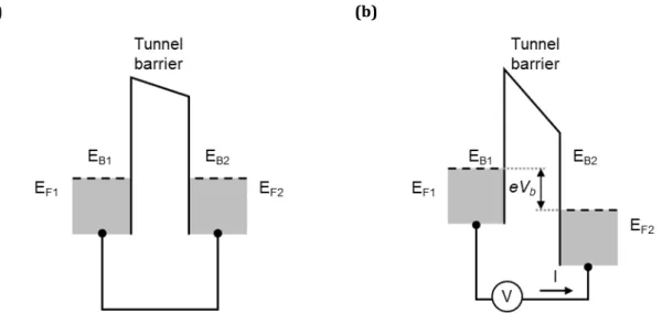
In 1991, Renaud and Alvarado introduced scanning tunneling microscopy-excited luminescence with nanometer resolution on III-V heterostructures [56,57]. This technique is referred to as scanning tunneling electroluminescence (STL) in the present work. It uses the tip of a scanning tunneling microscope (STM) as a source of electrons to inject carriers in a semiconductor sample. The emitted light resulting from the radiative recombination of the injected carriers is then detected. Figure 1.6 shows a schematic of the STL working principle.
Figure 1.6: Schematic of the working principle of STL. STM tip in proximity of the surface with
tunneling current flowing between tip and sample exciting luminescence in the semiconductor.
Renaud and Alvarado used this local luminescence technique to study the band bending profile and the conduction band discontinuities at the interfaces within p-doped AlxGa1-xAs/GaAs
heterostructures [57]. They describe STL in a three-step model [57]:
1) tunneling injection of carriers from the STM tip to the sample surface, 2) carrier transport in the semiconductor,
1 III-nitride semiconductors
The first step of this process is comparable to the description for standard STM. However, band-to-band radiative recombination of the injected carriers requires the presence of the counter charge. When injecting electrons from the tip to the semiconductor, p-doped samples have to be used. Band-to-band radiative recombination can only occur beyond the band bending region that forms near the surface. The applied bias voltage has to account for the electron being injected into the conduction band and transmitted beyond the surface depletion region. This requirement sets the bias voltage threshold 𝑉𝑡ℎ of luminescence onset to 𝑒𝑉𝑡ℎ> 𝐸𝐶 , with 𝐸𝐶 being the energy of the bottom of the conduction band in the bulk referred to the Fermi level. Comparable to the current transmitted through the metal layer in ballistic electron emission microscopy (BEEM) experiments, the integrated luminescence intensity follows a quadratic dependence on the applied bias voltage. Considering energy and momentum conservation parallel to the surface, an injection cone for the electrons crossing the depletion region to reach the bulk is described by [57]: 𝑠𝑖𝑛2𝛩𝑐 = 𝑚∗(𝑒𝑉 𝑡ℎ− 𝐸𝐶) 𝑚∗(𝛿 + 𝑒𝑉 𝑡ℎ− 𝐸𝐶) × 𝑒𝑉𝑡ℎ− 𝐸𝐶 𝛿 + 𝑒𝑉𝑡ℎ− 𝐸𝐶 .
The energy dependent effective mass 𝑚∗(𝐸) of the electrons accounts for the non-parabolicity of the band. The amplitude of the downward band bending is 𝛿. Outside this injection cone, electrons are reflected or trapped in the band bending region, leading to the nanometer resolution of STL. Using STL, Renaud and Alvarado achieved nanometer resolution in their measurements of the conduction band profiles on AlxGa1-xAs/GaAs heterostructures [57].
The application of STL has led to astonishing results from exciton trapping at localized defect states in organic semiconductors [58,59] and resonant energy transfer from the tunneling current to the excitons in 2D materials [60], to the evidence of photon emission in the visible range from quantum confined states in porous Silicon [61]. In nitride semiconductor heterostructures, Evoy et al. [62] and Manson-Smith et al. [63] applied STL to study the effect of defects on recombination. Their samples consisted of thick injection layers (respectively 100 nm in [62] and 200 nm in [63]) and a series of QWs in the active region in [62] and single QW capped by a GaN/AlGaN barrier in [63]. For a series of QWs, the emission spectra from the different QWs overlap each other leading to a summed signal. The single QW (SQW) used in [63] was buried 200 nm away from the surface, which broadened the injection cone of carriers and, therefore, leading to a summation of the emission from many localization regions. Hence, in both cases it was not possible to resolve the emission from single localized states.
We, therefore, propose to use a near-surface single GaN/InGaN/GaN QW to study localization effects induced by alloy disorder. Our experimental approach will be explained in detail in Chapter 2 Experimental Method, while the results gained on nitride semiconductors will be discussed in Chapter 3 Results.
2
Experimental method
In this chapter, we recall the basics of scanning tunneling microscopy and of scanning tunneling electroluminescence, which is a later development of the first. The experimental setups and the
measuring procedures that we developed are described in detail.
2.1
Techniques
2.1.1
Scanning tunneling microscopy
5Scanning tunneling microscopy (STM) is a well-established surface sensitive local probe technique. For its invention Gerd Binnig and Heinrich Rohrer were awarded with the Nobel Prize in Physics in 1986 [64]. STM excels for the ability to probe the electronic density of states down to the atomic scale. Its application enabled surface imaging with atomic resolution, atom manipulation, spectroscopy of the local density of states of surfaces and materials, as well as many other advancements in condensed matter physics.
STM is based on quantum mechanical tunneling through a barrier. Figure 2.1 offers a standard representation of tunneling through a potential barrier, e.g., vacuum or insulating layer, separating two conducting solids. When a bias voltage between the two materials is applied, a tunneling current flows through the barrier resulting from the overlap of the exponential tails of the electron wavefunctions on both side of the barrier.
(a) (b)
Figure 2.1: Tunneling through a barrier between two conducting solids with different work
function. (a) Without applied bias voltage and (b) with applied bias voltage.
In the highly simplified case, the solution of the Schrödinger equation inside the barrier is:
5 This is a short introduction to scanning tunneling microscopy. For more details, refer to the literature e.g.
Dawn A. Bonnell, Scanning Probe Microscopy and Spectroscopy (Theory, Techniques, and Applications) [65] or C. Julian Chen, Introduction to Scanning Tunneling Microscopy [67].
2 Experimental method
𝜓(𝑧) = 𝜓(0)𝑒−𝜅𝑧 with 𝜅 =√2𝑚(𝑉𝑏−𝐸)
ℏ ,
where Vb is the potential applied between the two sides of the barrier, E and m are respectively
the electron’s energy and mass.
The current I of the electrons tunneling through the barrier decays exponentially with the barrier thickness z:
I ∝ 𝑒−2𝜅𝑧 .
In an STM, the conducting material on one side of the barrier is an atomically sharp metallic tip commonly made out of Pt-Ir or W. The other side is the sample surface which is to be measured. Between the sample and the tip, a bias voltage is applied. The STM tip is brought in proximity of the sample surface, so that the overlap of their wave functions results in a tunneling current flow. The tunneling current is:
I = C𝜌𝑡𝜌𝑠𝑒𝑧⋅𝑘
1/2
,
for small voltages (V << work function of the material), with C a constant, and 𝜌𝑡 and 𝜌𝑠 being the density of states of the tip and of the surface, respectively [65]. Figure 2.2 illustrates a schematic of the working principle of an STM with the tunneling current flowing between the apex of the tip and one atom on the sample surface (highlighted in blue).
The position and motion of the tip in the three spatial directions x, y and z are controlled via piezo-electric devices (piezo scanners). The distance between the STM tip and the sample surface is controlled by a feedback loop with gain control. The feedback loop allows to adjusts the tip-to-sample distance to ensure a constant tunneling current (“constant current”-mode) or if it is switched off to keep an initial absolute tip altitude constant (the current and tip-to-sample distance while scanning thus varies). The latter is called “constant height”-mode. In the “constant
Figure 2.2: Schematic of the working principle of an STM. A bias voltage is applied between the
tip and the sample. The STM tip is moved by piezo scanner. A feedback loop controls the tip-sample distance. The tip z-motion is recorded as a function of the tip position in the xy-scanning plane allowing for the surface topography measurement with atomic resolution.
2 Experimental method
current”-mode, when scanning the tip over the surface, the tip motion maps the iso-joint density of states of the material’s surface. A second and larger set of piezo scanners enables movements to adjust the global xy-position of the tip on the sample (not shown in schematic).
2.1.2
Scanning tunneling electroluminescence
From the invention of STM, a large variety of scanning probe techniques have emerged. For example, atomic force microscopy, Kelvin probe force microscopy, scanning near-field optical microscopy, ballistic electron emission microscopy, and STL.
As already mentioned, STL consists of using the tip of an STM as a local source of electrons to inject carriers in a semiconductor and detecting the light emission resulting from the carrier recombination in the material.
Our goal is to study localization effects induced by alloy disorder in a near-surface InxGa1-xN/GaN
QW by STL. Due to the local nature of the tunneling injection, we assume that electrons reaching the QW populate a limited number of the disorder-induced localization regions [43], as schematized in Figure 2.3. In these conditions, it is expected to obtain a signature of the emission from the different localized states by measuring the electroluminescence spectrum as a function of the tip position.
Figure 2.3: Schematics of STL measurement in InGaN/GaN heterostructures. The bias is applied
between the tip and a gold pad on the sample surface to inject carriers in the semiconductor heterostructure and excite radiative recombination from the disordered QW. Contours of the localization regions calculated by the localization landscape theory are sketched in the QW plane.
2.2
Experimental setups
2.2.1
STL in ambient atmosphere
Our experimental setup in ambient atmosphere is based on an Omicron CRYOSXM with significant adaptations. These adaptations are implemented on the mechanics of the STM head, on the control and acquisition electronics, and on the software (partly performed and shown in [66]). The
2 Experimental method
Omicron CRYOSXM is inserted into an Oxford flow cryostat (Optistat SXM Bath) enabling STM measurements down to liquid helium temperature. The whole system is suspended inside a box shielded from acoustic noise and mechanical vibrations. A picture of this setup is shown in Figure 2.4.
Figure 2.4: Omicron CRYOSXM STL in ambient conditions (air) setup free swinging inside the
isolation box with homemade adaptions and spectrometer on the right-hand side.
In the original setup, the tip was fixed and pointed upwards while the sample was carried by the scanner with the sample surface to be studied facing the ground. To collect the emitted luminescence with a large aperture through the window at the bottom of the cryostat, we exchanged the position of the tip and the sample. The sample is now in a fixed position while the STM tip scans over the surface. The transparent nature of the samples (we are studying the emission of an InGaN QW inside a GaN structure grown on sapphire) enables to work in a
transmission geometry. A sample holder has been designed with an inserted optical lens of short
focal length (4 mm) and large numerical aperture of 0.6 (Thorlabs C610TME-A). A photo of the sample holder with the lens and contact pads is shown in Figure 2.5 (a). Figure 2.5 (b) displays the sample holder with a contacted sample and the STM tip in close proximity of the surface.
2 Experimental method
(a) (b)
Figure 2.5: (a) Homemade sample holder containing a collecting lens with short focal length and
contact clips. (b) sample placed on its holder and contacted via contact clips with STM tip close proximity to its surface.
The luminescence from the sample is collimated by the lens inside the sample holder. The lens-to-sample distance can be optimized with respect to the lens-to-sample thickness. The emitted light is transmitted through the window at the bottom of the cryostat and focused via an achromatic 10 mm diameter lens with 0.24 NA (Thorlabs AC060-010-A-NL) at the entrance of an optical fiber (Thorlabs, M114L02) with 0.22 NA and 600 µm core diameter. The optical fiber guides the light to the entrance slits of the spectrometer. Figure 2.6 shows a complete schematic of our STL setup.
Figure 2.6: Schematic of our complete STL setup in ambient atmosphere, including the
photoluminescence/alignment line and data processing.
We used two different spectrometers in our STL setup based on the Omicron CRYOSXM. The results at low tunneling currents of 2 nA presented in Chapter 3.2.3 were performed with a
2 Experimental method
Princeton Instruments IsoPlane SCT 320 spectrometer equipped with a 2D silicon detector. The resolution of this setup with fully opened slits is 35 meV. Starting from Chapter 3.3.2 (measurements at high tunneling current of 20 nA), we used a Horiba MicroHR Imaging Spectrometer with a Synapse EMCCD optimized for the UV to visible range. The slits of the spectrometers are closed to 600 µm giving a final resolution of 26 meV for the monochromator. The collection efficiency of the extracted light at the exit of the fiber is ~ 0.7%.
A typical topography measurement of a GaN surface (see 3.1.1. for sample details) recorded with this STM setup is shown in Figure 2.7, along with a surface profile showing terraces separated by bi- and mono-atomic steps [43].
(a) (b)
Figure 2.7: (a) 2.5 µm × 2.5 µm STM topography of a GaN surface. The inset shows a zoom on a
0.5 µm × 0.5 µm area around a hexagonal etch pit. (b) Surface profile showing terraces separated by bi- and mono-atomic steps [43].
2.2.2
STL in ultra-high vacuum
As we will see in detail in Chapter 3 Results, the Omicron CRYOSXM STM under ambient conditions was a suitable first candidate to study the disorder-induced localization effects in nitride semiconductors. Its operation in air makes it easy to access and manipulate the sample as well as the STM tip. However, operating an STM in air brings the disadvantage of surface contaminations. For example, the natural water film on the sample surface which could cause electro-chemical reactions (such as the formation of an oxide layer on the sample surface [66]) due to high current densities and high tunneling bias voltage necessary for STL measurements on nitrides. Operating the STL experiment under ultra-high vacuum (UHV) conditions would provide a better control of the surface and allow to extend the STL approach to other issues in semiconductor physics. This scenario is further discussed in Chapter 5 Conclusion and perspectives.
Consequently, we designed a new STL setup operating in UHV. The key figures for this experiment were set by the experience gained on the Omicron CRYOSXM setup. The light collection in transmission geometry provides a large aperture and high efficiency of the collection optics and leaves the space around the tip free. Therefore, we desire to keep the same geometry which led to
2 Experimental method
a small choice of commercially available STMs. Additionally, to the UHV condition and the light collection, the new STM setup should enable to perform temperature dependent measurements (cooling and heating) to study transport effects. Moreover, an optical access from the top to perform additional in-situ characterizations, and to improve the tip quality by in-situ sharpening techniques is necessary. Besides the hardware components, the software to drive this STM plays a considerable role since it needs to be adapted to the STL measurement procedure and synchronized with the spectroscopy setup.
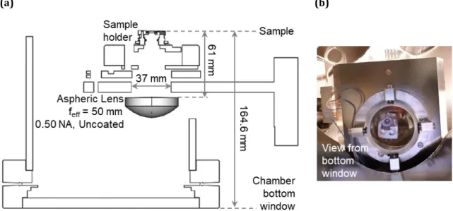
Considering all the requirements above, we opted for the RHK Technology’s UHV 300 Variable Temperature Ultra-High Vacuum Scanning Tunneling Microscope (VT UHV STM) with R9 electronics and customized adaptations. The sample holders in the RHK Beetle System naturally have an optical access from their backside and are, hence, well adapted for STL measurements in transmission geometry. Few adaptations still had to be carried out. First, a wider opening in the baseplate of the sample holder was drilled to allow a light collection with a larger aperture. Second, the pumping well below the chamber was removed and replaced by a view port which provides the optical access from outside the chamber to the back of the sample. Since the chamber was initially held by the pumping well, a specific fixation of the chamber to the floating support table was designed and the ion pump was mounted on a side free flange. Third, an optical breadboard was added below the chamber to fix the optical system for luminescence injection in the optical fiber. The final STL chamber is shown in the pictures of Figure 2.8. After baking the chamber, a base pressure of 3 × 10⁻¹⁰ mbar is currently reached.
2 Experimental method
For the optical collection, we designed a lens support which fixes a lens inside the UHV system behind the sample with the option to add a screen to shade the lens during sample annealing at a later stage. Figure 2.9 presents a cut through the technical drawing of the chamber showing the optical collection line and position of the lens as well as the final mounted result. For the light collection we chose an aspheric lens with an effective focal length of feff = 50 mm and 0.5 NA. This
configuration enables us to focus the divergent emission from the sample directly to the entrance of an optical fiber outside the chamber. The position of the optical fiber outside the chamber can be adjusted in xyz-position to optimize the alignment.
(a)
(b) (c) (d)
Figure 2.8: Pictures of customized RHK Technology’s UHV 300 Variable Temperature Ultra-High
Vacuum Scanning Tunneling Microscope, (a) view from the cryostat connection side on the main STM chamber, (b) STM head in scanning position on the sample holder inside the main chamber,
(c) view on the STM head in standby position inside the main chamber, (d) view from the transfer
2 Experimental method
(a) (b)
Figure 2.9: (a) Cut through the technical drawing of the STL chamber showing the optical access
as well as lens and lens position. (b) Picture of the final mount of the lens inside the STL chamber as seen from the bottom window.
In addition, we designed an adaptation for a laser from one of the top window flanges of the STL chamber, as shown in Figure 2.10 (a). The laser beam is focused on the sample surface in the area where the tip operates [Figure 2.10 (b)]. The photoluminescence spectrum is detected in transmission and optimized by adjusting the optical fiber position. The laser is incident on the sample surface with an angle of ~40° to minimize the collection of laser stray light in the fiber.
(a) (b)
Figure 2.10: (a) Adaptation for in-situ photoluminescence characterization: focused laser light is
injected through a view port onto the sample. (b) Focused laser spot on sample.
We will draw a comparison between the STL setup in ambient atmosphere and the STL setup under ultra-high vacuum in Appendix B.
2 Experimental method
2.3
Experimental procedure
2.3.1
STM tips
Preparing STM tips is commonly done by either a cut-and-pull technique or electrochemical etching. Both these techniques can be combined with further processing techniques to improve the tip’s quality. The metals typically used are W, which is processed by electrochemical etching, or alloys such as Pt-Ir, which allow tip fabrication both by the cut-and-pull technique or electrochemical etching. W tips are affected by surface oxidation which makes them unusable after time when running STM experiment in ambient air. Pt-Ir is less affected by the formation of an oxide on its surface which makes it the preferred choice if working in ambient conditions. In the work at hand, we used only Pt-Ir tips obtained by the cut-and-pull technique from a 0.25 mm diameter wire. The cut-and-pull technique to make STM tips will be explained in the following. As the name suggests, the cut-and-pull technique is based on a combination of cutting and pulling at the same time. The Pt-Ir wire is partially cut with a wire cutter. Simultaneously, the wire itself is pulled in opposite direction with a flat nose plier until the wire splits apart. This process is illustrated in Figure 2.11.
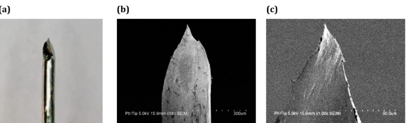
A sharp apex is needed to obtain a local probe for high resolution tunneling injection of electrons. Figure 2.12 shows optical microscopy and scanning electron microscopy (SEM) images of a typical tip obtained by the cut-and-pull technique. These rough examinations are, however, not sufficient to ensure the quality of the tip. Part of the tip conditioning is unavoidably empirical. For instance, the tip can be "sharpened" in-situ when performing STM measurements by fast and controlled hits against the surface. During these mild collisions with the surface the tip can pick up clusters from the surface and hence sharpen. This process, however, might also damage the tip [67].
Figure 2.11: Cut-and-pull technique to prepare STM tips. Arrows illustrating the movement to be
performed. The flat nose pliers pull back at the same time as the wire cutter cuts and pulls in the indicated direction.
2 Experimental method
(a) (b) (c)
Figure 2.12: Pt-Ir STM tip made by the cut-and-pull technique. Images taken with an optical
microscope (a) and taken via a scanning electron microscope (b) – (c).
Finally, the actual quality of the tip is checked best by acquiring STM topography images. Two examples of the atomic resolution achieved with two different tips in our setups is shown in the STM topography of highly oriented pyrolytic graphite (HOPG) in Figure 2.13.
(a) (b)
Figure 2.13: STM topography of HOPG recorded with 2 different tips revealing atomic resolution. (a) 7 nm × 7 nm, (b) 6 nm × 6 nm.
2.3.2 Taking an STL measurement
Once the STM tip is prepared, the sample is cleaned and contacted via the contact pad and one of the contact clips of the sample holder. The microscope head is inserted in the STM cryostat chamber or, respectively, the sample holder is inserted into the vacuum chamber of the RHK STL setup. The next step is the alignment of the tip relatively to the light collection setup used to perform the STL measurements. Due to potential drop on the surface of the sample, it has been proven beneficial to work as close as possible to the metal contact pad. Once the tip is positioned nearby the contact, the alignment is done by injecting the light of a halogen lamp through the collection fiber to illuminate the sample from the back through the substrate. The tip and light spot are then aligned to each other. A good alignment is achieved when the injected light reflects on the apex of the tip as shown in Figure 2.14.