HAL Id: hal-01473345
https://hal.archives-ouvertes.fr/hal-01473345
Submitted on 21 Feb 2017HAL is a multi-disciplinary open access archive for the deposit and dissemination of sci-entific research documents, whether they are pub-lished or not. The documents may come from teaching and research institutions in France or abroad, or from public or private research centers.
L’archive ouverte pluridisciplinaire HAL, est destinée au dépôt et à la diffusion de documents scientifiques de niveau recherche, publiés ou non, émanant des établissements d’enseignement et de recherche français ou étrangers, des laboratoires publics ou privés.
High Curie temperature Mn 5 Ge 3 thin films produced
by non-diffusive reaction
E. Assaf, A. Portavoce, K. Hoummada, M. Bertoglio, Sylvain Bertaina
To cite this version:
E. Assaf, A. Portavoce, K. Hoummada, M. Bertoglio, Sylvain Bertaina. High Curie temperature Mn 5 Ge 3 thin films produced by non-diffusive reaction. Applied Physics Letters, American Institute of Physics, 2017, 110 (7), �10.1063/1.4976576�. �hal-01473345�
High Curie temperature Mn
5Ge
3thin films produced by
non-diffusive reaction
E. Assaf, A. Portavoce*, K. Hoummada, M. Bertoglio, and S. Bertaina
IM2NP, CNRS/Aix-Marseille University, Faculté des Sciences de Saint-Jérôme case 142, 13397 Marseille, France
ABSTRACT
Polycrystalline Mn5Ge3 thin films were produced on SiO2 using magnetron sputtering
and reactive diffusion (RD) or non-diffusive reaction (NDR). In situ X-ray diffraction and atomic force microscopy were used to determine the layer structures, and magnetic force microscopy, superconducting quantum interference device and ferromagnetic resonance were used to determine their magnetic properties. RD-mediated layers exhibit similar magnetic properties as MBE-grown monocrystalline Mn5Ge3 thin films, while NDR-mediated layers
show magnetic properties similar to monocrystalline C-doped Mn5Ge3Cx thin films with 0.1 x 0.2. NDR appears as a CMOS-compatible efficient method to produce good magnetic quality high-curie temperature Mn5Ge3 thin films.
Keywords: Germanium, Manganese, thin film, ferromagnetic, reaction
*
The ferromagnetic compound Mn5Ge3 is expected to allow spin current injection in Ge
[1-4]. Consequently, the use of Mn5Ge3 thin films as ferromagnetic contacts on the source and
drain of Ge-based transistors is currently investigated in order to produce spintronic devices [4-6]. In the literature, Mn5Ge3 films are generally obtained via reactive diffusion,
reproducing the “Self-aligned silicide process” used in the Si Complementary metal oxide semi-conductor (CMOS) technology to produce ohmic contacts on transistor’s source, drain and gate [5-7]. Usually, an Mn film is deposited on an Ge substrate by molecular beam epitaxy (MBE) [6,8] before to be in-situ thermally annealed under ultra-high vacuum, in order to form a Mn5Ge3 layer at the Mn/Ge interface. The control of the annealing conditions (time,
temperature) allows the Mn5Ge3 layer to grow until the complete consumption of the initial
Mn layer, without the formation of the next compound in the phase formation sequence Mn11Ge8. The obtained Mn5Ge3 layer can be monocrystalline in epitaxy on Ge if the Mn film
is deposited on a Ge(111) substrate [6,8]. This self-aligned germanide process has the benefit to be compatible with industrial CMOS processes [5]. However, the Curie temperature (Tc) of Mn5Ge3 (~ 297 K) needs to be increased in order to obtain spin current injection at
temperatures higher than room temperature (RT) [5,9-10]. Usually, this is achieved using C [7,10-14] or Fe doping [15], the dopant being co-evaporated with Mn on the Ge substrate, complicating the deposition process. Furthermore, ultra-high vacuum MBE growth is not currently used in CMOS process lines, due to its significant production cost. Metallic films used for ohmic contact fabrication in CMOS technology are deposited by magnetron sputtering. In addition, one of the central drawbacks of Mn5Ge3 films grown on Ge is the
weak stability of the film, which can transform into Mn11Ge8 during a following annealing in
following transistor fabrication process steps [5]. Though, electrical spin injection in n-type Ge through a 2 nm-thick Al2O3 tunneling barrier was recently demonstrated, from a 40-nm
thick Mn5Ge3C0.8 polycrystalline layer grown by Mn, Ge, and C simultaneous magnetron
sputtering at 400 °C [4].
In this work, the magnetic properties of Mn5Ge3 films produced by means of two
different methods compatible with CMOS technology were investigated by magnetic force microscopy (MFM), superconducting quantum interference device (SQUID) and Ferromagnetic resonance (FMR). The magnetron sputtering technique [4,9] is shown to produce Mn5Ge3 films exhibiting similar magnetic properties as Mn5Ge3 films produced by
MBE. Furthermore, non-diffusive reaction (NDR) from an amorphous Mn0.625Ge0.375 film
leads to the formation of Mn5Ge3 films exhibiting higher Tc and better magnetic properties than Mn5Ge3 films produced by reactive diffusion (RD) of Mn and Ge layers deposited in
same conditions.
Two types of samples were prepared using a commercial magnetron sputtering system exhibiting a base pressure of 10−8 Torr and allowing simultaneous sputtering of three different targets. All the layers were deposited at RT in same conditions (Ar gas pressure…) using a 99.9999% pure Ar gas flow to sputter a 99.99% pure Ge target and a 99.9% pure Mn target. The sputtered layers were deposited on a SiO2 layer grown on an Si(001) substrate. The SiO2
layer acts as a diffusion barrier, preventing any intermixing between the layers and the Si substrate. For RD experiments, a 31 ± 2 nm-thick polycrystalline Mn layer was deposited on top of a 202 ± 13 nm-thick amorphous Ge layer. A sputtered Ge substrate was preferred to a commercial Ge wafer, allowing the results obtained with this sample to be fully comparable with the results obtained with the second type of sample (sputtered Ge in the two cases). For NDR experiments, a 45 ± 4.5 nm-thick amorphous Mn0.625Ge0.375 film was directly deposited
on the SiO2 layer. These two types of samples were in situ annealed under vacuum (10−6 Torr)
in an X-ray diffraction (XRD) setup following a heating ramp made of 5 °C per minute steps separated by 4 minutes-long XRD measurements at constant temperature (T), corresponding
to an average heating ramp of 1 °C min1. The XRD measurements were performed between RT and 400 °C in the Bragg-Brentano geometry, using a Cu K source (K = 0.154 nm). The
thicknesses of the films were measured before and after annealing using the X-ray reflectivity technique. The thickness (t) of the Mn5Ge3 film in contact with Ge obtained by RD was found
to be t ~ 48 ± 5 nm, while the thickness of the Mn5Ge3 film in contact with SiO2 obtained by
NDR was found to be t ~ 47 ± 2.5 nm. The sample surface topography was studied using a NT-MDT SMENA atomic force microscope (AFM) in air in non-contact mode. The magnetization component perpendicular to the sample surfaces was studied at RT by MFM in air, while the magnetic properties of the films were studied using SQUID and FMR measurements performed at RT and at 200 K with a conventional Bruker EMX spectrometer operating at f = 9.62 GHz.
In situ XRD measurements (not presented here) showed the same phase formation sequence as in the case of RD between a polycrystalline Mn film and an amorphous Ge layer deposited by e-beam evaporation [5]. Only two phases are observed in the sequence, the first phase being Mn5Ge3 and the second phase being Mn11Ge8. However, in the case of e-beam
evaporation, Mn5Ge3 was found to form at T ~ 210 °C and to transform into Mn11Ge8 at T ~
310 °C [5], while in the present case, Mn5Ge3 was found to form at ~ 240 °C and to be stable
up to temperatures as high as 400 °C. In the case of Mn5Ge3 formation by NDR, in situ XRD
measurements showed only the formation of Mn5Ge3 at T ~ 225 °C. Fig. 1 presents the
diffractograms obtained at RT after annealing the RD (a, red line) and NDR (b, black line) samples up to 400 °C. For the RD sample, three diffraction peaks corresponding to Ge (2 = 27.5°, 45.6°, and 53.9° corresponding respectively to the Ge planes (111), (220), and (311)) are easily detected (triangles in fig. 1). They correspond to the 200 nm-thick Ge layer that crystallized during annealing [5]. In addition, six diffraction peaks at 2 = 30.9°, 35.8°, 38.7°, 42.7°, 43.8°, and 56.7°, corresponding respectively to the atomic planes (111), (002), (210),
(211), (112), and (311) of Mn5Ge3 are also observed. No peak belonging to Mn11Ge8 can be
detected [5]. For the NDR sample, the same six diffraction peaks corresponding to Mn5Ge3
are also observed, with an additional peak at 2 = 46.3°, corresponding to the Mn5Ge3(202)
planes. The relative intensity of the Mn5Ge3 peaks is different in the two samples. For
example, the crystallographic direction exhibiting the maximum intensity in the RD sample is the (211), while it is the (002) direction in the NDR sample. Thus, the two Mn5Ge3 layers do
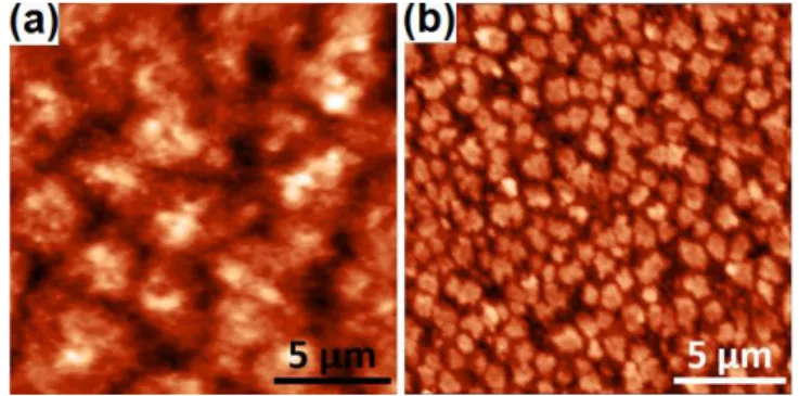
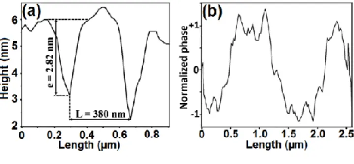
not possess the same texture. Fig. 2 presents AFM images of the sample surfaces. The grains are easily observed due to grain boundary (GB) grooving that occurred during annealing, resulting from equilibrium between the surface and interface energies at GBs [16-19]. For example, fig. 3a presents a one-dimensional profile (1D) measured on the NDR sample surface by AFM. GB grooves can exhibit a large width in the two samples (> 150 nm). However, their depth is about 3 nm that is negligible compared to the Mn5Ge3 layer thickness
(~ 50 nm). The average grain width (L) was determined considering that the lateral size of a given grain corresponds to the distance between the bottoms of the grooves located on each side of the grain [16-19], as presented in fig. 3a. L was averaged over all the grains detected on AFM images of 25 × 25 µm2 and 15 × 15 µm2 for the RD and NDR samples, respectively [20-21]. L ~ 1.09 µm and the surface roughness (root mean squared) r ~ 1.5 nm for the Mn5Ge3 layer produced by RD, while L ~ 0.4 µm and r ~ 1.2 nm for the Mn5Ge3 layer
produced by NDR. The Scherrer equation [22] applied to the XRD data of the RD- and NDR-mediated layers gives for the grain size in the direction perpendicular to the surface d = 51.6 nm and d = 47.7 nm, respectively. Thus, the two layers present a similar surface roughness, and in both cases, the grains are columnar (t ~ d) and their lateral size is larger than the Mn5Ge3 layer thickness (L t). Though, Mn5Ge3 grains are about two times larger in the layer
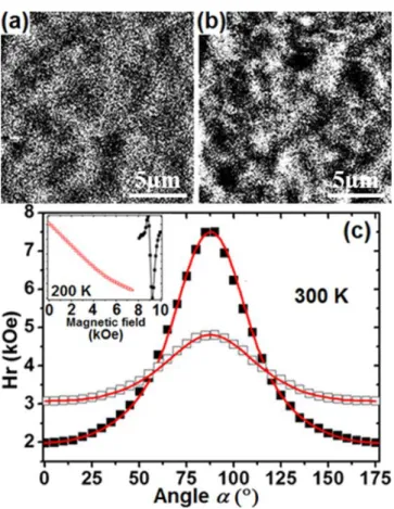
obtained by RD. Fig. 4a and 4b present the MFM images (phase contrast) obtained on the sample surfaces at RT without external magnetic field. Magnetic domains are visible on the
two samples, showing that the samples are ferromagnetic at RT. However, the magnetic domains are more easily detected on the NDR sample (fig. 3b), with a maximum contrast ~ 1.7°, than on the RD sample, with a maximum contrast ~ 1.4°. The domains do not follow the sample surface topologies. The average domain width is found to be ~ 0.65 ± 0.2 µm and ~ 0.39 ± 0.1 µm, and the average domain length is found to be ~ 1.5 ± 0.2 µm and ~ 0.9 ± 0.1 µm, on the RD and NDR samples, respectively. The angular () variation of the resonance field Hr is shown in fig. 4c. These measurements confirm that due to the film geometry, the samples possess a shape anisotropy with an easy axis in the direction parallel to the surface ( = 0°) and a hard axis in the direction perpendicular to the surface ( = 90°). Despite that the samples were produced using the same deposition technique in same conditions, the Mn5Ge3 layer produced by NDR exhibits a resonance field difference Hr
between the hard (Hr) and easy axis (Hr//) significantly higher than in the case of the Mn5Ge3
layer produced by RD. In addition, the results obtained on the RD sample are similar to the results obtained on a monocrystalline Mn5Ge3 layer in epitaxy on Ge(111) produced by RD of
an Mn layer deposited by MBE on a Ge(111) substrate [14]. For the latter, Hr// and Hr were found to be about ~ 2.7 and 5.0 kOe, respectively, giving Hr ~ 2.3 kOe at RT [14]. In our case, Hr// ~ 3.1, Hr ~ 4.8, and Hr ~ 1.7 kOe for the polycrystalline Mn5Ge3 layer obtained
by RD. Hr depends on the ferromagnetic layer Tc. For example, Hr ~ 2.3 kOe was shown to correspond to Tc = 315 10 K for the epitaxial MBE-mediated Mn5Ge3 layer [14]. This is
in agreement with the expected Tc ~ 297 K of the Mn5Ge3 compound, as well as with our
MFM measurements (fig. 4a) showing a faint signature of ferromagnetic domains at RT. Contrasting with Mn5Ge3 epitaxied layers [14], the FMR measurements can be well simulated
using the Chappert model (solid lines in fig. 4c) containing only two magnetic anisotropies [23]: the shape and magnetocrystalline anisotropies. This is probably due to the polycrystalline nature of the present Mn5Ge3 films. Using the RT Mn5Ge3 saturation
magnetisation M = 360 emu cm3 [24], the magnetocrystalline anisotropy constants (K1 and K2//) of the polycrystalline RD-mediated Mn5Ge3 layer were calculated considering a
gyromagnetic ratio /2 = 2.8 GHz kOe1 [23]. We found K1 = 0.57 × 10⁶ erg cm3, and K2// = 5.42 × 10⁴ erg cm3. FMR measurements compared to SQUID measurements performed on C-doped epitaxial MBE-mediated Mn5Ge3Cx layers showed that Hr ~ 3.7 kOe (Hr// ~ 2.3 and Hr ~ 6.0 kOe) for x = 0.1 corresponds to Tc = 345 10 K, and Hr ~ 7.0 kOe (Hr// ~ 1.6 and Hr ~ 8.6 kOe) for x = 0.2 corresponds to Tc = 450 30 K [14]. Hr// ~ 2.0, Hr ~ 7.5, and
Hr ~ 5.5 kOe in the polycrystalline Mn5Ge3 layer obtained by NDR (fig. 4c), which suggests
that the Tc in the NDR-mediated Mn5Ge3 layer is larger than in the RD-mediated layer, and is
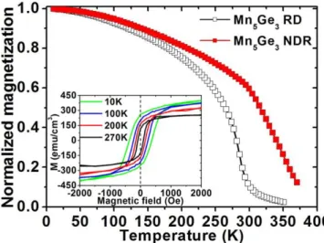
comprised between 345 and 450 K. SQUID measurements were performed on the samples in order to confirm the FMR measurements. As expected, the magnetization variations versus temperature presented in fig. 5 show that the Curie temperature is ~ 300 K and ~ 385 K, in the RD- and NDR-mediated Mn5Ge3 films, respectively. FMR measurements were also
performed at 200 K (not shown here). However, the signal from the RD-mediated layer being too broaden (red open symbols in the inset in fig. 4c), measurements could be performed only on the NDR-mediated Mn5Ge3 layer (black solid symbols in the inset in fig. 4c). We
measured Hr// ~ 1.3 kOe, Hr ~ 9.1 kOe, and Hr ~ 7.8 kOe in this layer at 200 K. The significant FMR signal difference at 200 K between the two Mn5Ge3 layers presented in the
inset in fig. 4c shows clearly that the NDR-mediated layer exhibits better magnetic properties than the RD-mediated layer [25].
Tc in Mn5Ge3 is mainly related to Mn-Mn atoms interactions [26], and thus, depends
on the distance between Mn atoms in the compound. This distance can be modified by stress and/or alloying with a third element. The Mn5Ge3 bulk compound possess a hexagonal
structure, with the standard (calculated) lattice parameters a = b = 0.7185 nm and c = 0.5053 nm [27]. These parameters were measured in the samples from the XRD data presented in
fig. 1. For the RD mediated layer, the lattice parameters were found to be a = b = 0.7158 nm and c = 0.5014 nm. For the NDR mediated layer, the lattice parameters were found to be a = b = 0.7135 nm and c = 0.5016 nm. These data are very similar, the difference between the measurements being in the sub-angstrom range (102 angstrom), it is related to measurement accuracy. Consequently, the Tc variations observed between the RD- and NDR-mediated samples cannot be explained by stress effect. In our case, there is no alloying effect, since Ge and Mn were the only elements sputtered on the substrates. However, sputtered layers are known to contain C and O atoms with concentrations that can reach several percent depending on the purity of the Ar gas and of the targets, as well as on the deposition rate and of the setup base pressure. The C doping effect allowing for Tc increase in Mn5Ge3(C) was shown to be of
electronic nature, interstitial C atoms in the Mn5Ge3 compound promoting the appearance of
the 90° ferromagnetic superexchange between Mn atoms [26]. Thus, the reason for the Tc difference between the two Mn5Ge3 layers could be related to a difference of C incorporation,
related to the two reaction types RD and NDR. Usually, RD allows impurities such as C and O to be pushed-out to interfaces and to GBs during the layer growth, allowing the formation of thin films significantly less contaminated than the initial sputtered layers [28]. At the opposite, atomic diffusion being not necessary during NDR [29], C incorporation could be more effective during this process, leading to a Tc increase in NDR-mediated Mn5Ge3 layers.
In conclusion, Mn5Ge3 layers were grown on SiO2 using thin film magnetron
sputtering followed by thermal annealing up to 400 °C. Two different reaction types were investigated: RD and NDR. Magnetron sputtering is shown to allow polycrystalline Mn5Ge3
layers, exhibiting similar magnetic properties as MBE-mediated monocrystalline layers in epitaxy on Ge(111), to be produced. RD-mediated Mn5Ge3 layers exhibit magnetic properties
magnetic properties as C-doped Mn5Ge3Cx layers with 0.1 x 0.2 and Tc ~ 385 K. The difference of magnetic properties between the layers produced by RD and NDR could be related to a difference of C incorporation in the Mn5Ge3 layers, RD leading to a layer
purification process decreasing C incorporation and, at the opposite, NDR supporting C incorporation. The NDR process appears as an interesting technique to produce low-cost high-Curie temperature Mn5Ge3 layers.
This work was supported by the French government through the program “Investissements d’Avenir A*MIDEX” (Project APODISE, no. ANR-11-IDEX-0001-02) managed by the National Agency for Research (ANR).
REFERENCES
[1] S. Picozzi, A. Continenza, and A.J. Freeman, Phys. Rev. B 70, 235205 (2004).
[2] R.P. Panguluri, C. Zeng, H.H. Weitering, J.M. Sullivan, S.C. Erwin, and B. Nadgorny, Phys. Stat. Sol. (b) 242, R67 (2005).
[3] Yu.S. Dedkov, M. Holder, G. Mayer, M. Fonin, and A.B. Preobrajenski, J. Appl. Phys.
105, 073909 (2009).
[4] I.A. Fischer, L.-T. Chang, C. Sürgers, E. Rolseth, S. Reiter, S. Stefanov, S. Chiussi, J. Tang, K.L. Wang, and J. Schulze, Appl. Phys. Lett. 105, 222408 (2014).
[5] O. Abbes, A. Portavoce, V. Le Thanh, C. Girardeaux, and L. Michez, Appl. Phys. Lett.
103, 172405 (2013).
[6] M. Petit, L. Michez, C.-E. Dutoit, S. Bertaina, V.O. Dolocan, V. Heresanu, M. Stoffel, V. Le Thanh, Thin Solid Films 589, 427 (2015).
[7] L.-A. Michez, F. Virot, M. Petit, R. Hayn, L. Notin, O. Fruchart, V. Heresanu, M. Jamet, and V. Le Thanh, J. Appl. Phys. 118, 043906 (2015).
[8] C. Zeng, S.C. Erwin, L.C. Feldman, A.P. Li, R. Jin, Y. Song, J.R. Thompson, and H.H. Weitering, Appl. Phys. Lett. 83, 5002 (2003).
[9] E. Sawatzky, J. Appl. Phys. 42, 1706 (1971).
[10] A. Spiesser, V. Le Thanh, S. Bertaina, and L.A. Michez, Appl. Phys. Lett., Vol. 99, 121904 (2011).
[11] M. Gajdzik, C. Sürgers, M.T. Kelemen, and H.v. Löhneysen, J. Magnetism and Magnetic Materials 221, 248 (2000).
[12] I. Slipukhina, E. Arras, Ph. Mavropoulos, and P. Pochet, Appl. Phys. Lett. 94, 192505 (2009).
[13] A. Spiesser, I. Slipukhina, M.-T. Dau, E. Arras, V. Le Thanh, L. Michez, P. Pochet, H. Saito, S. Yuasa, M. Jamet, and J. Derrien, Phys. Rev. B 84, 165203 (2011).
[14] C.-E. Dutoit, V.O. Dolocan, M. Kuzmin, L. Michez, M. Petit, V. Le Thanh, B. Pigeau, and S. Bertaina, J. Phys. D: Appl. Phys. 49, 045001 (2016).
[15] T.Y. Chen, C. L. Chien, and C. Petrovic, Appl. Phys. Lett. 91, 142505 (2007). C dopage
[16] E. Rabkin, L. Klinger, T. Izyumova, A. Berner, and V. Semenov, Acta mater. 49, 1429 (2001).
[17] A. Otsuki, Acta mater. 49, 1737 (2001).
[18] H. Yoshida, K. Yokoyama, N. Shibata, Y. Ikuhara, T. Sakuma, Acta Materialia 52, 2349 (2004).
[19] A. Ramasubramaniam, and V.B. Shenoy, Acta Materialia 53, 2943 (2005). [20] D. Nečas, P. Klapetek, Cent. Eur. J. Phys. 10, 181 (2012).
[21] A. Portavoce, K. Hoummada, F. Dahlem, Surface Science 624, 135 (2014).
[22] C. Eid, E. Assaf, R. Habchi, P. Miele and M. Bechelany, RSC Adv. 5, 97849 (2015). [23] C. Chappert, K. Le Dang, P. Beauvillain, H. Hurdequint, and D. Renard, Phys. Rev. B
34, 3192 (1986).
[24] A. Spiesser, Ph.D. Thesis, Aix-Marseille University, 2011.
[25] W. Platow, A.N. Anisimov, G.L. Dunifer, M. Farle, and K. Baberschke, Phys. Rev. B 58, 5611 (1998).
[26] I. Slipukhina, E. Arras, Ph. Mavropoulos, and P. Pochet, Appl. Phys. Lett. 94, 192505 (2009).
[27] L. Castelliz, Monatsh. Chem. 84, 765 (1953).
[28] K. Hoummada, I. Blum, D. Mangelinck, A. Portavoce, Appl. Phys. Lett. 96, 261904 (2010).
FIGURE CAPTIONS
FIG. 1. XRD measurements performed at RT after annealing the samples up to 400 °C using
an average heating ramp of 1 °C per minute: a) RD sample, and b) NDR sample.
FIG. 2. AFM measurements performed after annealing: a) RD sample, and b) NDR sample.
FIG. 3. 1D profiles measured after annealing on the NDR sample surface (on different
regions), a) by AFM and, b) by MFM.
FIG. 4. Magnetic measurements performed at 300 K, a) 5 × 5 µm2 MFM image obtained on the RD sample, b) 5 × 5 µm2 MFM image obtained on the NDR sample, and c) angular variation of the resonance field measured by FMR on the RD (open squares) and NDR (solid squares) samples. The red solid lines correspond to simulations using the Chappert model [20]. The inset shows the FMR signal ( = 90°) measured at 200 K on the RD (red open squares) and NDR (black solid circles) samples.
FIG. 5. Magnetization evolution versus temperature in the RD (open squares) and NRD (solid
squares) samples with a magnetic field of 0.01 T applied in-plane. The Curie temperature of the RD-mediated Mn5Ge3 layer is ~ 300 K, while it is ~ 385 K for the NRD-mediated layer
(linear approximation). The inset presents the M-H loop at 10 T 270 K for the NDR sample.
Figure 1 E. Assaf et al.
Figure 2 E. Assaf et al.
Figure 3 E. Assaf et al.
Figure 4 E. Assaf et al.
Figure 5 E. Assaf et al.