HAL Id: hal-01745718
https://hal.archives-ouvertes.fr/hal-01745718
Submitted on 20 Jul 2018
HAL is a multi-disciplinary open access
archive for the deposit and dissemination of
sci-entific research documents, whether they are
pub-lished or not. The documents may come from
teaching and research institutions in France or
abroad, or from public or private research centers.
L’archive ouverte pluridisciplinaire HAL, est
destinée au dépôt et à la diffusion de documents
scientifiques de niveau recherche, publiés ou non,
émanant des établissements d’enseignement et de
recherche français ou étrangers, des laboratoires
publics ou privés.
Oxide based resistive RAM: ON/OFF resistance
analysis versus circuit variability
Hassen Aziza, Haytem Ayari, Santhosh Onkaraiah, Jean-Michel Portal,
Mathieu Moreau, Marc Bocquet
To cite this version:
Hassen Aziza, Haytem Ayari, Santhosh Onkaraiah, Jean-Michel Portal, Mathieu Moreau, et al.. Oxide
based resistive RAM: ON/OFF resistance analysis versus circuit variability. 2014 IEEE International
Symposium on Defect and Fault Tolerance in VLSI and Nanotechnology Systems (DFT), Oct 2014,
Amsterdam, Netherlands. �10.1109/DFT.2014.6962107�. �hal-01745718�
978-1-4799-6155-9/14/$31.00 ©2014 IEEE
Oxide based Resistive RAM: ON/OFF Resistance
Analysis versus Circuit Variability
H. Aziza, H. Ayari, S. Onkaraiah, J-M. Portal, M. Moreau, M. Bocquet
IM2NP-UMR CNRS 7334, Aix-Marseille Université, Marseille, FranceTel: +33 491 054 782; Fax: +33 491 054 790
Abstract— A deeper understanding of the impact of variability on Oxide-based Resistive Random Access Memory (so-called OxRRAM) is needed to propose variability tolerant designs to ensure the robustness of the technology. Although research has taken steps to resolve this issue, variability remains an important characteristic for OxRRAMs. In this paper, impact of variability on OxRRAM circuit performances is analysed quantitatively at a circuit level through electrical simulations. Variability is introduced at the memory cell level but also at the peripheral circuitry level. The aim of this study is to determine the contribution of each component of an OxRRAM circuit on the ON/OFF resistance ratio.
Keywords-component; Resistive RAM; Oxide-based RAM (OxRRAM), variability
I. INTRODUCTION
A typical Resistive RAM (RRAM) device consists of two metallic electrodes that sandwich a thin dielectric layer serving as the ion transport and storage medium. The exact mechanism differs significantly among the different materials being used, but the common link among all RRAM devices is an electric field or heat causes ionic movements and local structural changes in the storage medium, which in turn causes a measurable change of the device resistance [1]. In RRAM, the data is stored as two or multiple resistance states of the resistive switching device and relies on a Metal/Insulator/Metal (MIM) stack that can be easily integrated into the Back-End Of Line (BEOL), paving the way for 3D technology.
Resistive switching in transition metal oxides was discovered in thin NiO films decades ago [2]. Since then, a large number of materials showing a resistive switching have been reported in the literature [3-4]. Among them, metal oxides as HfO2, NiO, TiO2 or Cu2O are promising
candidates due to their compatibility with CMOS processes. Oxide-based RAM elements (OxRRAMs) present a lot of interesting features like high integration density, high-speed operations (write/erase/read) and satisfactory reliability performances in terms of retention and cycling [5]. In OxRRAM memories, MIM structure are used as a single-bit memory cell, while the semiconductor transistor subsystem enables performing all the peripheral operations (input/output, coding/decoding, line driving, and sense amplification) [6].
Although OxRRAM-based devices have shown encouraging properties, challenges remain, among which the device variability (or reproducibility) is the main. Indeed, the variance from switching cycle to cycle and from device to device can be very large. For example, it has been experimentally demonstrated that such variability is in the range 2×-10× for the ON resistance and 5×-100× for the OFF resistance in Cu2-O-based devices [7]. Besides, MOSFET
mismatch in the transistor subsystem (digital and analog blocks) increases inherent variability of OxRRAM technology [8-9]. On top of that, sensitivity to Single Event Effects (SEEs) caused by a single energetic particle is also investigated [10-11].
In the literature, unipolar, bipolar and non-polar electrical behaviors are reported [1]. In the case of bipolar switching, addressed in this paper, bipolar voltage sweeps are required to switch the memory element (Fig. 1). In working conditions, after an initial electroforming process, the OxRRAM element may be reversibly switched between RESET (high resistance) and SET states (low resistance). Electroforming stage corresponds to a voltage-induced resistance switching from an initial very high resistance state (virgin state) to a conductive state. In Fig. 1, a typical I-V characteristic of a bipolar OxRRAM cell is presented. Resistive switching corresponds to an abrupt change between a High Resistance State (HRS or OFF state) and a Low Resistance State (LRS or ON state). This resistance change is achieved by applying specific voltage to the structure (i.e. VSET and VRES).
Based on the memory cell hysteresis presented in Fig. 1, in a first approximation, four OxRRAM critical reliability parameters can be considered: VSET, VRES, RHRS and RLRS.
Indeed, any variations of any of these parameters, among the cells in a memory array may lead to a limitation in the overall performance of the memory.
As a result of cell variability impact on OxRRAM cell parameters, circuit performance exhibits much wider variability [12-13]. This inherent drawback of the technology has to be investigated at a circuit level.
In this context, the presented study proposes an evaluation of the impact of variability on the ON/OFF resistance ratio. Section II presents the simulation circuit while section III analyses the contribution of each component of an OxRRAM circuit on the ON/OFF resistance ratio. Section IV concludes the paper.
II. SIMULATION CIRCUIT A. OxRRAM model
The proposed OxRRAM modeling approach relies on electric field-induced creation/destruction of oxygen vacancies within the switching layer. The model enables continuously accounting for both SET and RESET operations into a single master equation in which the resistance is controlled by the radius of the conduction pathways (
r
CF) [14]:(
)
kT V q Ea CF T k V q Ea CF CF CF b cell ox dOx b cell red dOx e r e r r dt dr − +⋅⋅ ⋅ ⋅ ⋅ ⋅ − − ⋅ ⋅ − ⋅ ⋅ − = α β α βRe 10Re 10 max (1)where βRedOx is the nominal oxide reduction rate, Ea is the
activation energy, αred and αox are the transfer coefficients
(ranging between 0 and 1), kb is the Boltzmann constant, T is
the temperature and Vcell the voltage across the cell.
Moreover, the model makes assumptions of a uniform radius of the conduction pathways, a uniform electric field in the cell and temperature triggered acceleration of the oxide reduction reactions (“redox”). Finally, the total current in the OxRRAM includes two components, i.e. one is related to the conductive species (IFC) and the other to the conduction through the oxide
(IOX).
(
)
(
CF CF OX CF OX)
x Cell CF r r L V I = ⋅π⋅ ⋅σ −σ +π⋅ 2 ⋅σ max 2 (2) HRS x Cell Cell HRS OX L V S A I β ⎟⎟ ⎠ ⎞ ⎜⎜ ⎝ ⎛ ⋅ = (3)where Lx is the oxide thickness, SCell is the total area of the
device, σOx the oxidation rate and σCF the reduction rate. To
take into account IOX trap assisted current (Poole-Frenkel,
Schottky emission, Space Charge Limited Current (SCLC)), a power law between the cell current and the applied bias is considered with two parameters AHRS and βHRS. Finally, the
total current flowing through the cell is:
OX CF Cell I I
I = +
(4)
ICF is the main contributor to LRS current (ILRS) and IOX is the
main contributor to HRS current (IHRS).
The memory cell compact model is calibrated on silicon. The model was confronted to quasi-static and dynamic experimental data before its implementation in electrical circuit simulators. As presented in Fig. 2a, after calibration, the model satisfactorily matches quasi-static and dynamic experimental data measured on actual HfO2-based memory
elements (TiN/Ti/HfOx/TiN stack reported in [15]). To
program a bipolar OxRRAM cell, a voltage ramp is needed. In Fig. 2b, the evolution of SET voltages as a function of the ramp speed is presented. The model implementation focused on this dependence which is crucial for the model to be confidently implemented in circuit simulators.
-1.5 -1.0 -0.5 0.0 0.5 1.0 10-9 10-8 10-7 10-6 10-5 10-4 10-3 0.0 0.5 1.0 10-9 10-7 10-5 10-3 10-1 101 103 105 Simu. Data [9] Set Reset (a) I Ce ll (A ) VCell (V) (b) T Se t VApp Simu. Data [9]
Fig.2 (a) I-V characteristic measured on HfO2-based devices [15] and corresponding simulation using a bipolar OxRRAM physical model. (b) Set
voltage as a function of the programming ramp
-1.5 -1.0 -0.5 0.0 0.5 1.0 10-9 10-8 10-7 10-6 10-5 10-4 10-3 Lines: Simu. Symbols: Data [9] I Ce ll (A ) VCell (V)
Fig.3 Measured and corresponding simulated I-V characteristic obtained from TiN/Ti/HfO2/TiN devices showing strong variation on RLHS and RHRS
Due to the stochastic nature of the switching process in OxRRAMs, leading to large variability, the OxRRAM model features a variability dependency.
The variation is chosen to fit experimental data as presented in Fig. 3 (I-V characteristic in logarithmic scale). The model
behavior (lines) is consistent with experimental data (symbols). HRS variation is generally larger than LRS variation for this technology. The manufacturing process of a TiN/Hf/HfO2/TiN stack is presented in [16]. Statistical variations in the switching parameter metrics such as VSET, VRESET, ROFF and RON have been examined in-depth in the recent past. The origin (“cause”) of all these variations in resistive switching memory are the microscopic transport of oxygen ions/vacancies [17] and the different permutations of filamentary clusters [18] they form during different SET-RESET cycles.
The cell variability modeling is based on OxRRAM card model parameters variation. The variation is chosen to feet experimental data. Variability is introduced through specific model parameters (i.e. βRedOx and βHRS parameters presented
respectively in Equ. 1 and Equ. 3). B. OxRRAM elementary circuit
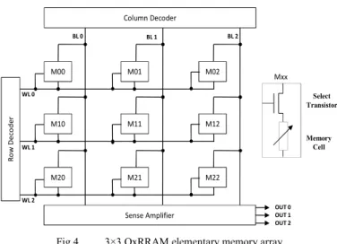
Fig. 4 presents the elementary array used for simulation which is constituted by a 3×3 1T/1R cell matrix, a row decoder, a column decoder and a sense amplifier for the read operation. The 1T/1R memory cell (one MOS transistor in series with one resistor) is seen as an effective alternative to replace embedded DRAM-based memory modules by substituting the capacitor by an OxRRAM resistor. The memory cell is modeled by the OxRRAM cell model presented in section II.A.
The variability analysis is conducted through Monte Carlo simulations. Each Monte Carlo simulation targets specific elements of the circuit: the resistive element, the select transistor, the decoding blocs and the sense amplifier. As a result, RON and ROFF distribution spreads are extracted. Thus,
the contribution of each element in terms of memory performance degradation is demonstrated. The study is conducted using a 28-nm Fully Depleted Silicon-On-Insulator (FDSOI) technology [19].
Memory array cells are first placed in a virgin state. Then, the memory array programming is done in 2 cycles. First, all memory cells are set (logical “1”), then the memory array is reset (logical “0”). RON value is extracted after the SET operation and ROFF after the RESET operation for each Monte Carlo run.
Variability introduced in the resistive element is chosen to feet experimental data (see Fig. 3) whereas variability of the transistor subsystem is given by the considered technology.
M00 M01 M02 M10 M11 M12 M20 M21 M22 Column Decoder Sense Amplifier OUT 0 OUT 1 OUT 2 Ro w D e co d e r BL 0 BL 1 BL 2 WL 0 WL 1 WL 2 Select Transistor Memory Cell Mxx
Fig.4 3×3 OxRRAM elementary memory array III. RESULTS
In this study, 4 different configurations are considered: the “ALL” configuration considers variability in the memory cell (resistive element and select transistor) and the peripheral circuits. In the “CELL” configuration, variability affects only the resistive element. In the “SELECT” configuration, variability affects only the OxRRAM select transistor. In the “NO CELL” configuration, variability affects only the peripheral circuits (transistor subsystem, including the select transistor). In this study, the impact of the select transistor variability is subject to special attention. Indeed, the select transistor compliance allows the control of the maximum available current during the set transition, impacting directly the ON/OFF resistance. Table I summarizes the 4 configuration to simulate.
TABLE I. SIMULATED CONFIGURATIONS
Configuration RUNS Elements under variability « ALL » 400 All circuit elements
« CELL » 400 Resistive element
« SELECT » 400 Select transistor
« NO CELL » 400 All elements excluding the resistive element Fig 5 presents the impact of variability of the whole circuit elements (resistive element and transistor subsystem: “ALL” configuration) on RON and ROFF distributions after 400 Monte
Carlo simulations. Note that ROFF distribution is much larger
than RON distribution. In order to discriminate the contribution
of each element of the circuit on ON/OFF resistances, a set of Monte Carlo simulations are performed with “CELL”, “SELECT” and “NO CELL” configurations.
« ALL » configuration
RON ROFF
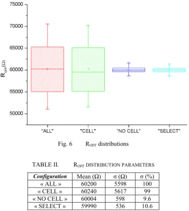
Fig.5 ON/OFF resistance distributions for the “ALL” configuration Fig.6 presents the impact of variability on ROFF
distributions (after RESET) for the 4 configurations. By comparing configuration “ALL” with configuration “CELL”, it appears clearly that the impact of cell variability is more important than the impact of the transistor subsystem variability. The third and fourth configurations (“NO CELL” and “SELECT”) shows that impact of transistors variability on ROFF is negligible. Besides, the contribution of the select
transistor variability is dominant in the peripheral circuit elements. Table II proposes a synthesis of results obtained in Fig. 6 (mean values, standard deviation and standard deviation ratio, reported on maximum standard deviation value).
Fig. 6 ROFF distributions
TABLE II. ROFF DISTRIBUTION PARAMETERS Configuration Mean (Ω) σ (Ω) σ (%) « ALL » 60200 5598 100 « CELL » 60240 5617 99 « NO CELL » 60004 598 9.6 « SELECT » 59990 536 10.6
Fig. 7 presents the impact of variability on RON distributions
(after SET) for the 4 configurations.
Fig. 7 RON distributions
TABLE III. RON DISTRIBUTION PARAMETERS Configuration Mean (Ω) σ (Ω) σ (%)
« ALL » 9674 724 100
« CELL » 9679 513 70.8
« NO CELL » 9642 550 78.7 « SELECT » 9713 570 75.9
Compared with Fig. 6, it appears clearly that the cell variability impact is less pronounced for low resistive states (LRS), which is a common feature of all OxRRAM technologies [20-23]. Moreover, the contribution of transistors variability is comparable to the contribution of the memory cell variability (see “CELL” and “NO CELL” configurations in Fig. 7). Once again, simulation results show that the impact of the select transistor is not negligible. Table III proposes a synthesis of results obtained in Fig. 7.
Fig.9 shows a comparison between RON and ROFF distributions.
Based on the considered technology, it is shown that resistance variability in RESET state is much more important than variability in the SET state. This variability is mainly due to the memory cell. In addition, the impact of the select transistor is non-negligible. This effect is visible in the SET state where the impact of the memory cell variability is much less important, making the select transistor variability critical.
IV. CONCLUSION
Variability in OxRRAM memories presents a major challenge for fabrication process and design engineers. In the proposed study, OxRRAM variability is evaluated based on an OxRRAM compact model included in an elementary memory array design. Simulation results show a signification impact of cell variability on the memory array ON/OFF resistances. Variability is introduced at the memory cell level but also at the peripheral circuitry level. The aim of this study is to determine the contribution of each component of an OxRRAM circuit on the ON/OFF resistance ratio. It has been demonstrated, based on a specific technology that variability in RESET state is mainly due to the memory cell. In SET state, impact of variability is less important, making the select transistor variability critical. This study underlines the need of variability tolerant designs to ensure the robustness of the technology.
REFERENCES
[1] J. Hutchby and M. Garner, Assessment of the Potential & Maturity of Selected Emerging Research Memory Technologies, ITRS – ERD/ERM Technology Work Groups Report on Emerging Research Memory Technologies (2010).
[2] S. Seo & al., “Reproducible resistance switching in polycrystalline NiO films”, Appl. Phys. Lett., Vol. 85, No. 23, p. 5655 (2004).
[3] F. Nardi, et.al, “Resistive switching by voltage-driven ion migration in bipolar RRAM Part I: Experimental study”, IEEE Transactions on Electron Devices, vol. 59, no. 9, pp. 2461–2467, 2012.
[4] S. Larentis, et.al “Resistive switching by voltage-driven ion migration in bipolar RRAM Part II: Modeling”, IEEE Trans. on Electron Devices, 59(9), pp. 2468–2475, 2012.
[5] M. J. Le & al., “A fast, high-endurance and scalable non-volatile memory device made from asymmetric Ta(2)O(5-x)/TaO(2-x) bilayer structures,” Nat. Mater., vol. 10, no. 8, pp. 625–630, 2011.
[6] H. Aziza & al, “Bipolar OxRRAM memory array reliability evaluation based on fault injection”, International Design and Test Workshop, pp. 78-81 (2011).
[7] An Chen & al., “Variability of resistive switching memories and its impact on crossbar array performance”, Proc. of the IEEE International Reliability Physics Symposium (IRPS), pp. MY.7.1 - MY.7.4, 2011. [8] Y. Joly, L. Lopez, JM. Portal, H. Aziza, Y. Bert, F. Julien, P. Fornara,
“Matching degradation of threshold voltage and gate voltage of NMOSFET after Hot Carrier Injection stress”, Microelectronics Reliability 51 (9), pp. 1561-1563, 2011.
[9] Y. Joly, L. Lopez, JM. Portal, H. Aziza, Y. Bert, F. Julien, P. Fornara, “Active “multi-fingers”: Test structure to improve MOSFET matching
in sub-threshold area”, International Conference on Microelectronic Test Structures, pp. 225-228, 2012.
[10] K. Castellani-Coulie, M. Bocquet, H. Aziza, JM. Portal, W. Rahajandraibe, C. Muller; “SPICE level analysis of Single Event Effects in an OxRRAM cell”, Latin American Test Workshop, pp. 1-5, 2013 [11] K. Castellani-Coulie, G. Micolau, H. Aziza, JM. Portal, “Analysis of
SEU parameters for the study of SRAM cells reliability under radiation”, Latin American Test Workshop, pp. 1-5, 2011
[12] H. Aziza & al, “Evaluation of OxRAM cell variability impact on memory performances through electrical simulations”, Non-Volatile Memory Technology Symposium (2011).
[13] H. Aziza & al, “Single-ended sense amplifier robustness evaluation for OxRRAM technology”, Proc. of the IEEE International Design and Test Symposium (IDT), pp. 1-5, (2013).
[14] M. Bocquet & al, “Compact Modeling Solutions for Oxide-Based Resistive Switching Memories (OxRAM)”, Journal of Low Power Electronics and Applications, 4 (1), pp. 1-14 (2014).
[15] T. Diokh, “Investigation of the Impact of the Oxide Thickness and RESET conditions on Disturb in HfO2-RRAM integrated in a 65nm CMOS Technology” in International Reliability Physics Symposium, 2013, pp. 3–6
[16] B.Govoreanu, & al., “10x10nm2 Hf/HfOx Crossbar Resistive RAM with Excellent Performance, Reliability and Low-Energy Operation”, Electron Devices Meeting, pp. 31.6.1-31.6.4, 2011.
[17] R. Degraeve, & al., “Dynamic ‘hour glass’ model for SET and RESET in HfO2RRAM”, Symposium on VLSI Technology (VLSIT), pp.75-76, 2012.
[18] N. Raghavan, R. Degraeve, L. Goux, A. Fantini, D.J. Wouters, G. Groeseneken and M. Jurczak, “RTN insight to filamentary instability and disturb immunity in ultra-low power switching HfOxand AlOxRRAM”, IEEE VLSI Technology Symposium (VLSI), T163-T164, 2013.
[19] C. Mazure, & al., “FDSOI: From substrate to devices and circuit applications”, ESSCIRC, p.45-51, (2010).
[20] M. Boquet & al., “Robust Compact Model for Bipolar Oxide-Based Resistive Switching Memories”, IEEE Transactions on Electron Devices,Vol. 61, Iss. 3 (2014).
[21] S. Hamdioui, H. Aziza, G. Ch. Sirakoulis, “Memristor based memories: Technology, design and test”, in Design & Technology of Integrated Systems In Nanoscale Era Conference, pp. 1.7, 2014.
[22] N.Z. Haron, S. Hamdioui, “On defect oriented testing for hybrid CMOS/memristor memory”, Asian Test Symposium (ATS), pp. 353-358, 2011.
[23] N.Z. Haron, S. Hamdioui, “DfT schemes for resistive open defects in RRAMs”, Proceedings of the Conference on Design, Automation and Test in Europe (DATE), pp. 799-804, 2011.