HAL Id: hal-02100273
https://hal-amu.archives-ouvertes.fr/hal-02100273
Submitted on 15 Apr 2019
HAL is a multi-disciplinary open access
archive for the deposit and dissemination of
sci-entific research documents, whether they are
pub-lished or not. The documents may come from
teaching and research institutions in France or
abroad, or from public or private research centers.
L’archive ouverte pluridisciplinaire HAL, est
destinée au dépôt et à la diffusion de documents
scientifiques de niveau recherche, publiés ou non,
émanant des établissements d’enseignement et de
recherche français ou étrangers, des laboratoires
publics ou privés.
SEU Sensitivity of Junctionless SOI MOSFETs-based 6T
SRAM Cells Investigated by 3D TCAD Simulation
Daniela Munteanu, Jean-Luc Autran
To cite this version:
Daniela Munteanu, Jean-Luc Autran. SEU Sensitivity of Junctionless SOI MOSFETs-based 6T SRAM
Cells Investigated by 3D TCAD Simulation. ESREF Conference, Oct 2015, Toulouse, France.
�hal-02100273�
SEU Sensitivity of Junctionless SOI MOSFETs-based 6T SRAM
Cells Investigated by 3D TCAD Simulation
D. Munteanu
a, J.L. Autran
a,*a Aix-Marseille Univ, CNRS, Univ Toulon, IM2NP (UMR 7334), Faculté des Sciences – Service 142,
Avenue Escadrille Normandie Niémen, F-13397 Marseille Cedex 20, France
Abstract
The Junctionless (JL) Single-Gate SOI (JL-SOI) technology is potentially interesting for future ultra-scaled devices, due to a simplified technological process and reduced leakage currents. In this work, we investigate, for the first time, the radiation sensitivity of JL-SOI MOSFETs and 6T SRAM cells. A detailed comparison with JL Double-Gate (JL-DG), inversion-mode (IM) SOI (IM-SOI), and IM-DG MOSFETs has been performed. 3-D simulations indicate that JL-SOI MOSFETs and SRAM cells are naturally less immune to radiation than the other structures.
Corresponding author.
[email protected]
Tel: + 33 (0)413 594 627; Fax: +33 (0)491 288 531
SEU Sensitivity of Junctionless SOI MOSFETs-based 6T SRAM
Cells Investigated by 3D TCAD Simulation
D. Munteanu
a, J.L. Autran
a,** Corresponding author. [email protected] Tel: + 33 (0)413 594 627; Fax: +33 (0)491 288 531
1. Introduction
As the MOSFET is scaling down, the sensitivity of integrated circuits to radiation coming from space or present in the terrestrial environment has been found to seriously increase [1]. For ultra-scaled devices entering in the area of nanoelectronics, natural radiation at ground level is presently inducing one of the highest failure rates of all reliability concerns [2]. In particular, ultra-scaled memory integrated circuits have been found to be more sensitive to single-event-upset (SEU) induced by ionizing particles.
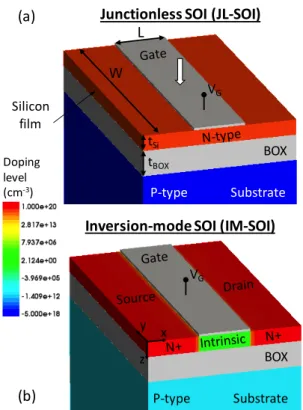
To meet the roadmap requirements in the nanometre scale, several promising technological solutions have been proposed, such as the Fully-depleted Single-Gate SOI technologies (FDSOI) fabricated with ultra-thin silicon bodies. FDSOI devices show enhanced performances in terms of channel potential control, reducing short-channel (SCE) and floating body effects (FBE). A new concept of MOSFET without junctions, called junctionless (JL) MOSFET has been proposed these last years and experimentally validated [3,4,5]. A JL MOSFET designed with a single-gate SOI structure (JL-SOI, Fig. 1a) is an SOI transistor with the same type of semiconductor throughout the entire silicon film, including the source, channel and drain regions. JL-SOI devices present a real advantage since their fabrication process is simplified compared to the conventional process: there are no doping gradients in the device [5] and no semiconductor-type inversion. In addition, the junction leakage currents are totally
suppressed and the off-state current (IOFF) is uniquely
controlled by the gate, which could be very attractive for ultra-short devices.
From a radiation-sensitivity point of view, the high doping level in the film of a JL MOSFET could have a negative impact on its immunity to single events,
BOX Substrate P-type
Inversion-mode SOI (IM-SOI)
Doping level (cm-3)(b)
Junctionless SOI (JL-SOI)
(a)
Substrate P-type BOX VG VG tSi W Silicon filmL
tBOX x y zFig. 1. Schematic description of the simulated JL-SOI (a) and IM-SOI (b) MOSFETs. For a better view spacers and
isolation oxides are not shown.
because floating body effects are expected to be strong. This was confirmed by our previous works [6,7] concerning the radiation-induced transient behaviour of JL Double-Gate (JL-DG) MOSFETs. In the present work, we investigate, for the first time, the radiation sensitivity of JL-SOI, in terms of bipolar gain of individual devices and SEU sensitivity of six-transistor (6T) SRAM cells. A detailed comparison with JL-DG, mode (IM) FDSOI (IM-SOI), and inversion-mode double-gate (IM-DG) MOSFETs and 6T SRAM cells has been also performed.
2. Simulation details
Figure 1 shows schematic 3-D descriptions of the simulated JL-SOI and IM-SOI devices. JL-SOI devices are designed with 100 nm gate width, 6 nm-thick silicon film and 0.9 nm-thick gate oxide. The entire
silicon film is uniformly n-type doped at 1019 cm-3;
there are no highly-doped source/drain regions. A 10 nm-thick buried oxide (BOX) and a thick silicon
substrate doped at 5x1018 cm-3 have been also
considered. IM-SOI (Fig. 1b) devices have an intrinsic channel; source and drain regions are highly n-type doped and the doping profile in these regions is uniform. The silicon film, BOX and silicon substrate of IM-SOI have the same geometrical parameters as those
of JL-SOI. The silicon substrate is lowly-doped at 1016
cm-3. IM-DG and JL-DG structures are based on real
devices reported in [8]. The silicon film of IM-DG and JL-DG has the same geometrical parameters and doping profiles as the silicon film of IM-SOI and JL-SOI, respectively, with the notable exception that two gates connected together control the channel potential. These four different structures have been first simulated with 20 nm-channel length, considering a power supply voltage of 0.75 V. These devices have been calibrated on the ITRS LP; to facilitate the comparison, the gates work functions have been finely
tuned to achieve the same IOFF for all devices.
Secondly, additional simulations have been carried out for other channel lengths and power supply voltages. 3-D numerical simulations have been performed with the DESSIS device simulator from Synopsis Inc. [9]. The main models used in simulation are: SRH and Auger recombination models, Fermi-Dirac carrier statistics, hydrodynamic model for the carrier transport, mobility model including the dependence on the carrier energy, lattice temperature and doping level and impact ionization model depending on carrier energy. The ion strike was simulated using the DESSIS HeavyIon module [9]. The electron-hole pair column created in the device by the ion strike is modeled using a carrier-generation function which has a Gaussian radial distribution with a characteristic radius of 20 nm and a Gaussian time distribution, centered on 10 ps and having a characteristic width of 2 ps.
3
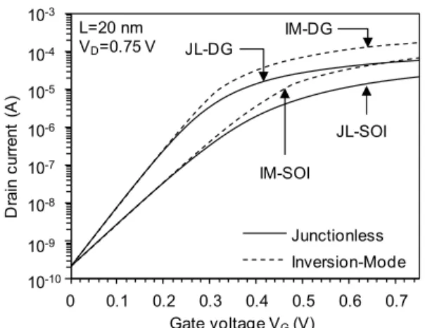
. Static characteristics of individual devicesThe simulated steady-state drain current characteristics of JL-SOI, IM-SOI, JL-DG and IM-DG are plotted in Fig. 2. The devices have the same
0 0.1 0.2 0.3 0.4 0.5 0.6 0.7 Dr ai n cu rr en t (A ) Gate voltage VG(V) Junctionless Inversion-Mode 10-10 10-9 10-8 10-7 10-6 10-5 10-4 10-3 JL-SOI IM-SOI IM-DG JL-DG L=20 nm VD=0.75 V
Fig. 2. Drain current as a function of gate voltage for JL-SOI, IM-JL-SOI, JL-DG and IM-DG. The gate workfunction
of each device has been tuned to obtain the same IOFF.
off-state current, but different subthreshold swings and on-state currents. While double-gate devices (both JL-DG and IM-JL-DG) have near ideal subthreshold swings (65 mV/dec), SOI devices have a much higher subthreshold swing (90 mV/dec) because the single-gate configuration reduces the control by the single-gate of the channel potential and increases the parasitic short-channel effects compared to a double-gate configuration. JL-SOI has the lowest on-state current because the highly-doped silicon film degrades the mobility. The highest on-state current is obtained in IM-DG, due to the combination of a double-gate structure and an intrinsic channel; this structure has the advantage to maximize the carrier mobility.
4
. Single-event transients4.1. Drain current, collected charge and bipolar gain
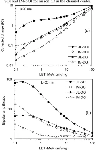
Figure 3 shows the drain current transient resulting from an ion hit in the channel center of JL-SOI and IM-SOI devices. The time variations of the collected charge are also reported on the same figure. The drain current transient peak and width are higher in JL-SOI than in IM-SOI, probably due to a higher bipolar gain. In addition, the drain current decay after the ion strike is slower for JL-SOI than for IM-SOI. The reason is that the floating body effects are more important in JL-SOI than in IM-JL-SOI, due to the high doping level in the JL-SOI film (since the device channel is intrinsic in IM-SOI). The collected charge and the bipolar amplification as function of the ion LET are plotted in Figs. 4a and 4b. The values obtained in [6] for JL-DG and IM-DG devices are also reported in these figures
0 0.5 1 1.5 2 2.5 3 3.5 Co lle ct ed c ha rg e (f C) Dr ai n cu rr en t (A ) Time (s) JL-SOI IM-SOI 10-13 10-12 10-11 10-10 10-9 10-8 10-7 10-6 10-10 10-9 10-8 10-7 10-6 10-5 10-4 L=20 nm LET=10 MeV.cm2/mg
Fig. 3. Drain current transient and collected charge in JL-SOI and IM-JL-SOI for an ion hit in the channel center.
0.01 0.1 1 10 0.1 1 10 100 Co lle ct ed c ha rg e (f C) LET (MeV.cm2/mg) JL-SOI IM-SOI JL-DG IM-DG L=20 nm 1 10 100 0.1 1 10 100 Bi p o la r a m p lif ic at io n LET (MeV.cm2/mg) JL-SOI IM-SOI JL-DG IM-DG L=20 nm
Fig. 4. Collected charge and bipolar amplification as function of LET in JL-SOI and IM-SOI MOSFETs for an
ion hit in the channel center.
for comparison. As expected, the bipolar gain is higher for JL-SOI due to stronger FBE compared to IM-SOI. The bipolar gain decreases when the LET increases because the parasitic bipolar transistor enters in the high-injection regime. At very high LET, the bipolar
60 55 50 45 40 35 30 25 20 10 0 Ion hit location Heavy-Ion Charge Density (cm-3)
Fig. 5. 3-D profile of heavy-ion charge density in the silicon film of JL-SOI for an ion hit at x=30 nm and LET=1 MeV.cm2/mg. Other positions for the ion strike considered in
this work are also indicated. For a better view of the film, gate material, spacers and isolation oxide are not shown.
0.1 1 10 0 10 20 30 40 50 60 Bi p o la r a m p lif ic at io n x (nm) JL-SOI IM-SOI JL-DG IM-DG LET=5 MeV.cm2/mg
Fig. 6. Bipolar gain in JL-SOI, SOI, JL-DG and IM-DG as a function of the ion hit location.
gain in JL-SOI decreases rapidly and becomes close to the values obtained in IM-SOI, JL-DG and IM-DG.
4.2. Dependence on the ion hit location
We also studied the dependence of the bipolar gain on the ion hit location along the channel (x axis). Several locations are considered between the source contact (x=0) and the drain contact (x=60 nm), as illustrated in Fig. 5. The 3-D profile of the heavy ion charge density in the silicon film is also shown in Fig. 5 for an ion hitting the film at x=30 nm (channel center). The current transient have been simulated for each x location and the collected charge was extracted from this transient. The bipolar gain is then obtained at a given LET for each x value. Figure 6 plots the bipolar gain dependence on the ion hit location for the four studied devices. The bipolar gain is always higher
in JL-SOI than in IM-SOI, but has similar
dependences on the ion hit location for all devices.
(a)
5
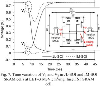
. SEU in 6T SRAM cells: critical charge, threshold LET and scaling trendsFor the four technologies, the 6 transistors of the SRAM cell (inset in Fig. 7) were entirely simulated in the 3-D device domain with the Synopsis/DESSIS module and were connected via the Mixed-Mode module [9]. Before simulating the SRAM cell we have determined for each technology the worst-case condition in terms of x location (along the channel) of the ion hit in the OFF-state NMOS. The worst-case location is the x location for which the collected charge is the highest. The worst-case x locations were found to be x=40 nm for both JL-SOI and IM-SOI devices. In the following, we used these worst-case locations for all SRAM cell simulations.
The time variations of the voltages extracted at
nodes 1 and 2 (V1 and V2) for LET=3 MeV.cm2/mg are
shown in Fig. 7 for JL-SOI and IM-SOI SRAM cells. For this LET value, the JL-SOI SRAM cell has flipped, while the IM-SOI SRAM cell did not flip.This result gives a first indication on the radiation hardness of JL-SOI technology: the SEU threshold LET of JL-JL-SOI SRAM cell will be lower than that of IM-SOI, which means that the JL-SOI is more sensitive to radiation than the IM-SOI technology.
The SEU threshold LET (LETth) of each cell was
obtained by varying the ion strike LET until the SRAM cell was observed to upset. As expected, the critical
charge Qcrit=0.126 fC and LETth=1.35 MeV.cm2/mg
are lower for the JL-SOI SRAM than for IM-SOI
SRAM cell (Qcrit=0.205 fC and LETth=3.15
MeV.cm2/mg, [7]). In order to explain these results, we
remind that Qcrit increases with the equivalent
capacitance of the struck node (CN), with the supply
voltage (VDD) and with the maximum current of the
on-state PMOS transistor (IPMOS), as explained in
[10,11]. In our study, all cells are operating at the same
VDD. CN is the same for JL-SOI and IM-SOI SRAM
cells, but IPMOS is lower in JL-SOI than in IM-SOI; this
then explains why Qcrit is lower in JL-SOI than in
IM-SOI SRAM cell. Qcrit and LETth of JL-SOI are also
lower than those corresponding to JL-DG (Qcrit=0.309
fC and LETth=3.64 MeV.cm2/mg) and IM-DG
(Qcrit=0.51 fC and LETth=7.48 MeV.cm2/mg) obtained
in [7].
Finally, we investigated the dependence of LETth
on the channel length, the power supply and, for
JL-SOI SRAM cells, the film doping level. LETth obtained
for two channel lengths are shown in Fig. 8. Additional
results for different VD values and doping levels and a
detailed discussion will be included in the full paper.
-0.1 0 0.1 0.2 0.3 0.4 0.5 0.6 0.7 0.8 0 5 10 15 20 25 30 35 40 45 Vo lta g e (V) Time (ps) JL-SOI IM-SOI V1 V2
Fig. 7. Time variation of V1 and V2 in JL-SOI and IM-SOI
SRAM cells at LET=3 MeV.cm2/mg. Inset: 6T SRAM
cell. 0 1 2 3 4 5 6 7 8 9 10 11 JL-SOI 50nm JL-SOI 20nm IM-SOI 50 nm IM-SOI 20 nm JL-DG 50 nm JL-DG 20 nm IM-DG 50 nm IM-DG 20 nm
Threshold LET, LETth(MeV.cm2/mg)
Fig. 8. Threshold LET of JL-SOI, SOI, JL-DG and IM-DG SRAM cells for two channel lengths, L=20 and 50 nm.
References
[1]. R.C. Baumann, IEEE Trans. Device Mater. Reliab., vol. 5, no. 3, pp. 305-316, Sept. 2005.
[2]. S. Mitra, P. Sanda, and N. Seifert, IEEE VLSI Test Symposium, 2008.
[3]. C.-W. Lee et al. Applied Physics Letters 94 (2009) 053511.
[4]. J.P. Colinge et al. Nature Nanotechnology 5 (2010). [5]. A. Kranti et al. Proc. ESSDERC, 2010, p. 357. [6]. D. Munteanu and J.L. Autran. IEEE Trans. Nucl. Sci.
59 (2012) 773.
[7]. D. Munteanu and J.L. Autran. Microelectronics Reliability, vol. 54, pp. 2284-2288, 2014.
[8]. M. Vinet et al. IEEE Electron Dev. Lett. 26 (2005) 317.
[9]. Synopsys Sentaurus TCAD tools, Available online: http://www.synopsys.com/products/tcad/tcad.html. [10]. P. Roche et al. IEEE Trans. Nucl. Sci. 46 (1999) 1354. [11]. S.M. Jahinuzzaman et al. IEEE Trans. Very Large
Scale Integr. (VLSI) Syst. 17 (2009) 1187.
WL VDD BL BL Access transistor NMOS Access transistor NMOS NMOS ON NMOS OFF PMOS OFF PMOSON “2” “1” V2 Ionizing particle V1