HAL Id: hal-01788964
https://hal-amu.archives-ouvertes.fr/hal-01788964
Submitted on 9 May 2018
HAL is a multi-disciplinary open access
archive for the deposit and dissemination of
sci-entific research documents, whether they are
pub-lished or not. The documents may come from
teaching and research institutions in France or
abroad, or from public or private research centers.
L’archive ouverte pluridisciplinaire HAL, est
destinée au dépôt et à la diffusion de documents
scientifiques de niveau recherche, publiés ou non,
émanant des établissements d’enseignement et de
recherche français ou étrangers, des laboratoires
publics ou privés.
based on SiGe random metasurfaces
Mohammed Bouabdellaoui, Simona Checcucci, Thomas Wood, Meher
Naffouti, Robert Paria Sena, Kailang Liu, Carmen Ruiz, David Duché,
Judikaël Le Rouzo, Ludovic Escoubas, et al.
To cite this version:
Mohammed Bouabdellaoui, Simona Checcucci, Thomas Wood, Meher Naffouti, Robert Paria Sena,
et al.. Self-assembled anti-reflection coatings for light trapping based on SiGe random metasurfaces.
Physical Review Materials, American Physical Society, 2018, 2 (3), pp.035203.
�10.1103/PhysRevMa-terials.2.035203�. �hal-01788964�
Self-assembled anti-reflection coatings for light trapping based on SiGe random metasurfaces
Mohammed Bouabdellaoui,1,2, Simona Checcucci,1,3,4,†Thomas Wood,1,‡,∗Meher Naffouti,1,5,∗∗, Robert Paria Sena,1Kailang Liu,1 Carmen M. Ruiz,1David Duche,1Judikael le Rouzo,1Ludovic
Escoubas,1Gerard Berginc,6 Nicolas Bonod,7Mimoun Zazoui,2Luc Favre,1 Leo Metayer,1
Antoine Ronda,1 Isabelle Berbezier,1David Grosso,1Massimo Gurioli,1and Marco Abbarchi?1
1
CNRS, Aix-Marseille Universit´e, Centrale Marseille, IM2NP, UMR 7334, Campus de St. J´erˆome, 13397 Marseille, France
2
Laboratory of Physics of Condensed Matter and Renewable Energy,
Faculty of Sciences and Technology, Hassan II University of Casablanca, 146 Mohammedia, Morocco
3
European Laboratory for Nonlinear Spectroscopy (LENS), 50019 Sesto Fiorentino, Italy
4
Dipartimento di Fisica ed Astronomia, Universit´a degli Studi di Firenze, 50019 Sesto Fiorentino, Italy
5
Laboratoire de Micro-opto´electronique et Nanostructures Facult´e des Sciences de Monastir Universit´e de Monastir 5019 Monastir, Tunisia
6
Thales Optronics, Elancourt, France
7
Aix-Marseille Universit´e, CNRS, Centrale Marseille, Institut Fresnel, Marseille, France (Dated: January 25, 2018)
We demonstrate a simple self-assembly method based on solid state dewetting of ultra-thin silicon films and germanium deposition for the fabrication of efficient anti reflection coatings on silicon for light trapping. Via solid state dewetting of ultra-thin silicon on insulator and epitaxial deposition of Ge we fabricate SiGe islands with a high surface density, randomly positioned and broadly varied in size. This allows to reduce the reflectance to low values in a broad spectral range (from 500 nm to 2500 nm) and a broad angle (up to 55 degrees) and to trap within the wafer a large portion of the impinging light (∼40%) also below the band-gap, where the Si substrate is non-absorbing. Theoretical simulations agree with the experimental results showing that the efficient light coupling into the substrate mediated by Mie resonances formed within the SiGe islands. This lithography-free method can be implemented on arbitrarily thick or thin SiO2layers and its duration only depends on the sample
thickness and on the annealing temperature.
I. INTRODUCTION
Efficient anti-reflection coatings (AR) have been inten-sively studied with many different approaches having been explored for this purpose1–3, such as multi-layered thin-films4,5, graded index matching via surface texturing with
micro- and nano-structures6–11, plasmonic metasurfaces12–14
and more recently, metasurfaces15–21 based on ordered
ar-rays of sub-micrometric dielectric antennas (dielectric Mie resonators22–28). Depending on the application of the AR different aspects (lowest value of the total reflectance, broad spectral range, broad acceptance angle, transparency or light trapping) determine the optimal features and fabrication method.
A convenient and efficient solution for enhancing light absorption relies on the exploitation of disordered structures13,29–33. The superior AR properties of
disor-dered systems account for the importance of this approach with respect to its ordered counterparts and it has been re-cently proposed20 and implemented19 using dielectric Mie
resonators. Such results, obtained via top-down methods,19
demonstrate that combining disorder and Mie resonators pro-vides efficient AR coatings at visible frequencies. How-ever, the ease of fabrication at affordable prices on reasonable timescales, are major requirements for realistic devices imple-mented on large scales and conventional top-down fabrication processes are unable to meet such criteria.
Random metasurfaces offer the basis for the development of less costly and large-scale bottom-up fabrication methods based on self-assembly. One viable and promising route is solid-state dewetting of ultra-thin films of metals18,34–41 and
semiconductors,42–46a natural phenomenon exploited for the self-assembly of high-quality photonic structures. The insta-bility giving rise to the dewetting phenomenon in thin films is mediated by the surface diffusion of atoms and occurs upon annealing at high temperature (even well below the melt-ing point of the material)47–58. Arrays of well separated is-lands, featuring a random spatial organization and a relatively large spread of sizes and shapes can be produces. The po-tential of this method in semiconductors has not been com-pletely exploited and, for example, AR coatings formed by self-assembly have not yet been reported. In fact, one of the main limits of this method is the relatively low density of the dewetted particles: in solid state dewetting, as in other self-assembly methods for 3D nanostructures (e.g. Stranski Kras-tanov growth in IV-IV and III-V compounds) a linear depen-dence links the initial thickness of the Si(Ge) layer and the final size (and density) of the dewetted islands59. This feature naturally leads to large inter-particle distances and limits the exploitation of dewetting for nanophotonics.
In this work, we report on the implementation of a self-assembly method based on dewetting and epitaxial growth for the fabrication of AR coatings. We manage to overcome the well-known limitations of most common self-assembly pro-cesses: the correlation between size and density of the islands. Furthermore, in contrast with previous reports of SiGe dewet-ting where marked spatial anisotropies affected the size distri-bution of the islands,44,60,61in our samples large and small par-ticles are perfectly mixed, providing a homogeneous arrange-ment of randomly positioned islands. The epitaxial growth during dewetting represents a step forward towards increasing the density of large particles capable of sustaining Mie
reso-nances.
We demonstrate efficient AR coatings both at visible and near-infrared frequencies, based on Mie resonances from high-density, randomly organized, SiGe-islands. Finite differ-ence time domain simulations (FDTD) highlight the resonant effect leading to the enhanced coupling and light-trapping of the impinging light towards the underlying Si wafer. A sys-tematic and quantitative comparison of our metasurfaces with thin films-based AR based on thin films highlights the superior performance of our approach in enhancing the light coupling within the underlying Si wafer, a useful trait for photovoltaic and detector applications.
Similar approaches in the literature15include ad hoc Si
3N4
conformal layers on top of the Mie resonators. In our ap-proach we extend this idea to a double layer of Si3N4 and
SiO2on the islands and on the backside of the samples. Thus,
we target specific wavelength ranges optimizing the AR for below band-gap frequencies, where the total reflectance (Rtot)
reaches 7-20%, and for above band-gap frequencies, where Rtotis reduced to few percentages. Angle-resolved
measure-ments confirm that these properties are maintained within an acceptance angle of about ±55 degrees.
We systematically address the different phenomena deter-mining the spectral features of our AR coatings providing a precise discrimination between the main photometric param-eters: total reflectance, specular reflectance, total transmis-sion and reflected scattering. We show that in our dielectric metasurfaces (also when covered with conformal layers15) the
dominant contribution to Rtot comes from nearly-isotropic,
backscattering whereas that of specular reflectance is only a few per cent of it. Monitoring the total transmission Ttot
for below band-gap frequencies allows to highlight a relevant light trapping within the substrate (Ttot+ Rtot< 100%).
The paper is organized as follows: in section II we ad-dress the main advantages and issues of solid state dewetting as a self-assembly method for Si- and SiGe-based Mie res-onators and we provide a description of the built-in morpho-logical and structural properties of the samples under inves-tigation. In sectionIIIwe provide a deep characterization of the spectroscopic features of the SiGe-based random meta-surfaces, addressing the light management in terms of total reflection, total transmission, light trapping, angular and po-larization dependent reflection and finally discriminating be-tween reflected scattering and reflected diffusion. We address both cases of bare islands and islands covered with confor-mal layers of SiO2 and Si3N4 providing a theoretical
inter-pretation of the results and a systematic comparison with the performances of conventional flat layers as ARs. In section
IVwe discuss the relevance of our findings putting them in the context of dielectric ARs based on ordered Mie resonators and in sectionVwe draw the conclusions.
II. METHODS
A. SOLID STATE DEWETTING FOR SiGe-BASED MIE RESONATORS
Intrinsic features of solid state dewetting of silicon films are set by the initial thickness of the thin, crystalline layer the period of the underlying Rayleigh-like instability, determin-ing all the built-in structural parameters of the islands, such as their density, size and equilibrium shape44,50,52,54,62. All
these properties can be modified by adding Ge before, during or after dewetting42–45,60,61,63 potentially providing full con-trol over their physical properties. However, in SiGe-based samples, Si-rich and Ge-rich particles are spatially separate, leading to large inhomogeneities of the morphological prop-erties over micrometric distances44,60,61that make this method
unsuitable for performing devices.
A relatively large vertical aspect ratio (η = h/r, where h is the particle’s height and r = d/2 is the half of its base size) is necessary for the formation of intense and sharp res-onances in dielectric Mie resonators64. While η remains low
in pure Si islands, it is higher in SiGe Si45,61. Here it is worth mentioning that the larger extinction coefficient of Ge with respect to Si at short wavelengths leads to enhanced losses (Supplementary Information SI Fig.SI. 2). However, theoreti-cal simulations65,66and practical implementations45,67,68have
unambiguously demonstrated the relevance of Ge for dielec-tric Mie resonators, at least for wavelengths larger than ∼500 nm.
From this picture it emerges that solid state dewetting of SiGe has a great potential for nanophotonics on large scales being a spontaneous phenomenon, but a convincing demon-stration of its performances is still missing. In what follows we show that a modified dewetting protocol allows to over-come the above mentioned limitations, providing a clearcut demonstration of the relevance of this method for the imple-mentation of SiGe-based Mie resonators on large scales.
B. EXPERIMENTAL
In order to overcome the intrinsic features of solid state dewetting of Si (low particles density and small η) we mod-ified the fabrication process by adding a large amount of Ge during the annealing step (300 monolayers MNLs at 800◦C, Fig.1a)). An accurate description of the fabrication process is reported in the SI along with a detailed investigation of SEM, TEM and AFM imaging of the fabricated samples is reported in SI (Fig.SI. 1 and relative discussion). From this structural investigation, we highlight: i) a random formation of the islands and a complete lack of spatial organization (as accounted for by the Fourier transform of a SEM image of sample II in the bottom inset of the central panel of Fig.1
b)); ii) a homogeneous distribution of large and small islands perfectly mixed together eventually showing a bimodal size distribution (Fig.1b)); iii) a lack of elongation of the islands along preferential crystallographic directions or a more pro-nounced symmetry for a family of islands44,60,61; iv) presence
3 of dislocations in both families of particles (Fig.SI. 1 f) and
g)). All these features are unique of this fabrication procedure and very similar results were obtained with samples grown in slightly different experimental conditions (e.g. at 780◦C) accounting for the robustness of the approach (not shown).
FIG. 1. Sample fabrication and particles’ size distribution. a) Dia-gram of the UT-SOI sample composition (12 nm of monocrystalline Si atop 20 nm of buried oxide, BOX) and description of the fabri-cation steps (i-iv). The bottom part describes the annealing cycle in the ultra-high vacuum (UHV) of the molecular beam reactor and the Ge deposition steps. Additional details of the fabrication process are provided in the Methods section. b) Statistical distribution of par-ticle size for sample I (top panel), II (central panel) and III (bottom panel). The insets show high-resolution SEM images of the dewetted samples. For sample II inset shows also the two-dimensional Fourier transform of a 9×9 µm2SEM image.
After dewetting and Ge supply, we deposited conformal layers of SiO2and Si3N4on top of the islands as well as on
the back face of the samples via plasma enhanced chemical vapor deposition. This step allows the optimization their anti-reflection properties as detailed later. The list of the samples and their features are summarized in TableI.
From AFM images (Fig.SI. 1 c), d) and e)) we highlight rather large geometrical aspect ratios η exceeding 0.745,61 of
bare SiGe islands and progressive smoothing of the samples’ roughness when increasing the thickness of the conformal lay-ers (e.g. the root mean square, RMS goes from ∼58 nm for sample II up to ∼35 nm for sample II-C, Fig.SI.1c), d) and e)).
TABLE I. List of samples with corresponding thickness of the SiO2
and Si3N4layers deposited on top of the SiGe islands (T) and on the
backside (B). All the reported thicknesses are expressed in nm. Sample T SiO2 T Si3N4 B Si3N4 B SiO2
I 0 0 0 0 I-A 0 130 100 100 I-B 0 100 100 100 I-C 0 70 100 100 II 0 0 0 0 II-A 120 120 80 80 II-B 100 100 80 80 II-C 80 80 80 80 III 0 0 0 0 III-A 0 130 100 100 III-B 0 100 100 100 III-C 0 70 100 100
III. OPTICAL CHARACTERIZATION AND SIMULATIONS
A description of the instruments and methods used for spec-troscopy is reported in the devoted section in the SI. The total reflectance Rtotof a Si wafer is determined by the refractive
index contrast with air, and by its thickness: for frequencies below the Si band-gap, the transparency of the material calls into play the reflection from the backside of the wafer. This determines a sharp increase of Rtotat about 1050 nm (Fig.2
a)). This increased value of Rtotcan be quantified in about
15-20% by simulating the reflection from the top face and from both top and bottom faces of a thick Si slab (respectively thick, purple line and thin, orange line in Fig.2a)).
The total reflectance Rtotfor a dewetted 12 nm thick SOI
is compared to that of a Si wafer (Fig.2b)). The small effect of the dewetted sample on the impinging light implies that per se, dewetting is not suitable for AR. Samples I, II and III with SiGe island however, show a pronounced AR effect with re-spect to the bare Si wafer (Fig.2b)). At frequencies larger than the Si band-gap the value of Rtot is about 4-12%, whereas
at larger wavelengths, this value rises to about 25-30% due to the transparency of the substrate and the back-face reflec-tion. We observe that samples I and III feature an enhanced light coupling in the substrate at near-infrared frequencies and more pronounced fluctuation of Rtotwith respect to II, which
springs from their particles’ larger average size and the more pronounced bimodal size distribution (Fig.1b)).
While the minimum of Rtot for bare SiGe islands is not
very low, the most remarkable feature of the AR effect of our metasurface is its extension to all the investigated frequencies with a very smooth spectral dependence. In fact, even if con-ventional ARs based on thin film coatings can provide lower values of Rtotat specific wavelengths, they fail in matching
the performances of our AR when considering the full spec-trum from visible to near-infrared. These features are system-atically investigated in the SI Fig.SI. 6 a), b) and c) where the spectra of simulated interferential ARs based on a SiO2
single layer, a Si3N4 single layer and a SiO2 on Si3N4
FIG. 2. Total reflectance Rtotfor Si- and SiGe-based metasurfaces.
a) Rtot in the full investigated spectral range for a Si wafer.
Ex-perimental data, black circles; theoretical simulation for the top face only, thick purple line; theoretical simulation for the both top and bottom faces, thin, orange line. The shaded area highlights the tran-sition from above- to below band-gap frequencies. b) Experimental data for Rtotmeasured on: Si wafer (gray line and shaded area), bare
Si islands (empty black squares) and bare SiGe islands sample I, II and III (respectively green circles, red squares and blue triangles). c) Total transmission Ttot(blue squares) and total transmission plus
total reflection Ttot+ Rtot(black line) for samples III. The error in
the measured light intensity is less than 2% in at longer wavelengths where the white lamp used for illumination is less intense.
III. While the average value of Rtotfor the best interferential
layer is above 26%, the SiGe-based metasurfaces are always below 25% (SI Fig.SI. 6 g), h), i) and j)). A summary of this investigation is shown in tableII.
Another relevant parameter necessary for defining the range of uses of a device is its total transmission Ttot. Bare SiGe
is-lands exhibit values of Ttot between about 35% and 60% in
the range 1200 to 2500 nm (Fig.2c)). By adding to Ttotthe
corresponding value of Rtot, we can see that a significant
por-tion of light is not transmitted nor reflected (Ttot + Rtot <
100%, Fig.2c)): about 40% of the total at 1200 nm is retained within the wafer (see also the data summarized in tableII). We interpret it as a light-trapping phenomenon already reported in similar systems based on dielectric Mie resonators21: the
pres-ence of 3D resonant scatterers on the sample surface imposes strong modifications to the propagation of the impinging light beam, leading to its partial trapping within the wafer. This feature represents a very important characteristic of our AR
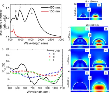
FIG. 3. FDTD simulations. a) Scattering intensity of an individ-ual island having base size of 150 nm (vertical aspect ratio 1/2). b) Scattering intensity of an individual island having base size of 450 nm (vertical aspect ratio 1/2). c) Near-field maps of the intensity of the electric field (|E|) and magnetic field (|H|) at 650 nm for the small particle simulated in a). The white lines highlight the shape of the island and the BOX. d) Near-field maps of the intensity of the electric field and magnetic field at 750 nm for the large particle sim-ulated in b). e) Near-field maps of the intensity of the electric field and magnetic field at 960 nm for the large particle simulated in b). f) Comparison between the measured Rtotfor samples I, II and III
and the FDTD simulation taking into account a random distribution of small (150 nm in diameter) and large (450 nm in diameter) SiGe islands.
and differentiates them from to conventional flat AR where, at these frequencies, Ttot + Rtot = 100% (not shown) and
no light trapping is possible irrespective of the performance in terms of AR (see also tableII). Importantly, the possibility to enhance the light absorption could be a valuable tool for extending the quantum efficiency of Si-based light detectors (such as CCD cameras) in this frequency range.
FDTD simulations were used to model the experimental findings (see the dedicated section the SI for details). They were first used to address the scattering intensity of individual small and large islands (respectively diameter d = 150 nm and d = 450 nm). The scattering intensity of small islands feature a sharp peak at ∼650 nm (α, Fig.3a) and b)). The electric and magnetic field intensity maps at 650 nm, respectively show that |E| is rather confined below the island within the buried oxide (BOX), whereas |H| is well channeled into the sub-strate (Fig.3b)). These features are quite similar to what was shown for SiGe islands.45 However, in the present study the
very thin BOX favors a more efficient light coupling within the Si wafer.15,64 The scattering intensity of large islands ex-hibit three main peaks in the investigated spectral range (β, γ and δ, Fig.3a), c), d) and e)). As for the previous case of small islands, the field intensity maps at ∼750 nm, ∼960 nm
5
FIG. 4. Below band-gap anti-reflection coating: samples I-A, -B,-C and III-A, -B and -Ca) From the top to the bottom panel: total re-flectance Rtotat quasi-normal incidence for samples I-A and III-A,
I-B and III-B, and I-C and III-C. b) From the top to the bottom panel: total transmission Ttot(blue squares) and Ttot+ Rtot(black line) at
quasi-normal incidence for samples III-A, III-B and III-C. The error in the measured light intensity is less than 2% in at longer wave-lengths where the white lamp used for illumination is less intense.
and ∼1600 nm, show that |E| is rather confined within the BOX, whereas |H| is well coupled into the substrate. These simulations show that SiGe-based Mie resonators are able to channel light from the ambient in the substrate thanks to the presence of resonantly confined fields extending in the under-lying Si wafer. Furthermore, the spread in size and the large density of the particles allows for a broad and smooth light coupling.
Simulations of Rtot on randomly distributed resonators
of two size-family show rather strong fluctuations between ∼18% and 1% in a spectral interval spanning from ∼400 nm to 1100 nm (black line in Fig.3f); for Rtotwe limit our
inves-tigation to above band-gap frequencies as the FDTD method does not allow to easily take into account the effect of the backside of the sample. Despite the rough approximations used for describing the particles size distribution in FDTD simulations, the overall agreement with experiments is fairly good (Fig.3 f)). Clearly, the presence of many differently sized particles in experiments smooths the features of Rtot,
but its average value in simulations and experiments are quite similar.
A complete and precise assessment of the AR properties, should go beyond the values of Rtotand Ttotand include also
the angular dependence of the reflected intensity, polarization properties, as well as a precise discrimination between light diffusion and specular reflectance. Improved performances with respect to the bare SiGe islands are obtained for all the samples when covered with conformal single or double lay-ers made of Si3N4and SiO215(TablesIandII). Samples I-A,
-B -C and III-A, -B and -C were optimized for below band-gap frequencies: the total reflectance remains between 7% and 20% (Fig.4a)) whereas it varied between 25% and 35% for the
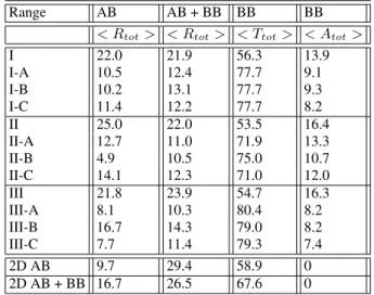
TABLE II. Values of < Rtot > for above band-gap frequencies
(AB: 300-1050 nm) and for the full investigated range (AB + BB: 300-2500 nm), < Ttot> and < Atot>=< 1 − Ttot− Rtot>
(ab-sorbed light) for below band-gap frequencies (BB: 1200-2500 nm), are reported for all the investigated SiGe-based samples. Same quan-tities are calculated via transfer matrix method for two flat interfer-ential double layers optimized for above band-gap frequencies (2D AB: 65 nm SiO2on 65 nm Si3N4) and for the full investigated range
(2D AB + BB: 145 nm SiO2 on 145 nm Si3N4). The values
rela-tive to our random metasurfaces are extracted form the experimental data whereas those relative to the flat layers are from simulations as shown in Fig.SI. 6 and 7.
Range AB AB + BB BB BB < Rtot> < Rtot> < Ttot> < Atot>
I 22.0 21.9 56.3 13.9 I-A 10.5 12.4 77.7 9.1 I-B 10.2 13.1 77.7 9.3 I-C 11.4 12.2 77.7 8.2 II 25.0 22.0 53.5 16.4 II-A 12.7 11.0 71.9 13.3 II-B 4.9 10.5 75.0 10.7 II-C 14.1 12.3 71.0 12.0 III 21.8 23.9 54.7 16.3 III-A 8.1 10.3 80.4 8.2 III-B 16.7 14.3 79.0 8.2 III-C 7.7 11.4 79.3 7.4 2D AB 9.7 29.4 58.9 0 2D AB + BB 16.7 26.5 67.6 0
bare samples (Fig.2b)). The different thickness of the confor-mal Si3N4coatings allows for a slight tuning of the minimum
of Rtot(e.g. from ∼1500 nm for sample I-C up to ∼2000 nm
for sample I-A). For sample III a more pronounced dip in Rtot
is observed in a narrower spectral range (up to 7%) owing to the presence of larger particles on sample III with respect to sample I (Fig.1b)).
Remarkably, when taking into account the full investigated spectral range spanning from visible to near-infrared frequen-cies, these metasurfaces outperforms conventional flat ARs (SI Fig.SI. 6 d), f) and j)). While the best double layer coat-ing features an average Rtotof about 26%, our samples are in
the 8-13% range. A summary of this investigation is shown in TableII.
Finally, as for the bare SiGe islands case, we estimate the light trapping for sample III-A, -B and -C (Fig.4c)). For these samples, covered with a conformal layer and with additional AR on the backside, Ttotis in the range of 60%-80% and it is
enhanced with respect to the bare SiGe islands (Fig.2c)). Ttot
+ Rtotincreases monotonically providing a light trapping of
about 20% at 1200 nm up to negligible values at 2500 nm (see also TableII). Thus, in spite of a better performance in terms of Rtot owing to the layers on the backside of the wafer, at
these frequencies, the light trapping is about two times less ef-fective for capped islands with respect to the bare case (Fig.2
c) top panel and Fig.4c)). This is an important observation in view of the exploitation of these structures for specific appli-cations where light trapping should be enhanced with respect
to transparency.
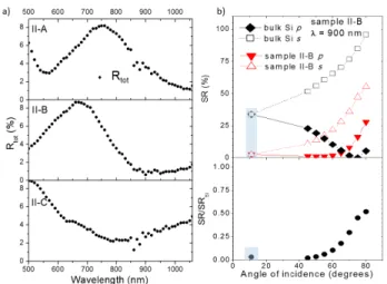
FIG. 5. Above band-gap anti-reflection coating: sample II-A, -B and -C.a) From the top to the bottom panel: total reflectance Rtot
at quasi-normal incidence for samples II-A, II-B and II-C. b) Top panel: specular reflectance SR for s- (open symbols) and p-polarized (full symbols) incident beam for sample II-B (triangles) and Si wafer (squares). SR for a beam incident on the sample surface at angles larger than 45 degrees is measured with an ellipsometer. SR at 11 degrees (shaded) is obtained from Rtotin graph a) and it thus also
contains the reflected scattering (Rtot= SR + RD, see also Fig.4).
Thus it represents an overestimation of SR. Bottom panel: Specular reflectance SR at 900 nm for sample II-B as a function of the inci-dence angle normalized to SR of Si wafer at the same wavelength. The error in the measured light intensity is less than 1%.
Samples II-A, II-B and II-C were optimized as AR for fre-quencies above the Si band-gap (tableIand Fig.5). For all these samples, Rtotcan reach values as small as a few %
ac-counting for the good performances of the AR coating. A tuning of the minimum of Rtot is possible thank to the
dif-ferent thicknesses of the additional conformal coatings. This leads to a shift in the minimum of Rtot from about 850 nm
for sample II-C up to 1050 nm for sample II-A. Thus, also in this narrower spectral range, the effect of the additional con-formal layers deposited atop the SiGe islands is to improve the AR properties of a factor of two or more with respect to bare islands. Furthermore, at normal incidence, sample II-B is more than a factor of two more performing than a double layer composed of SiO2on Si3N4(SI Fig.SI. 7 and TableII).
Angle-resolved measurements of the specular reflectance SR are collected with an ellipsometer (thus disregarding the reflected scattering RD, Fig.5b)). Averaging the specular re-flectance for s and p polarizations and normalizing this value to that one measured on a Si wafer allows to observe an excel-lent AR performance up to about 55 degrees (Fig.5b) bottom panel).
In order to address the composition of the reflected light in terms of scattered and specular reflection we take into account the case of sample II-B for above band-gap frequencies. The reflected scattering (RD, defined as the total reflection minus the specular reflection: RD = Rtot- SR) at quasi-normal
in-cidence and integrated over the half solid angle is compared to the corresponding value of Rtot(Fig.6a)). The similar values
and spectral features of Rtot and RD allow us to conclude
that most of the reflected light can be ascribed to the reso-nant backscattering from the SiGe Mie resonators distributed over the half solid angle atop the sample. The difference be-tween Rtot and RD represents the specular reflectance SR
and seems to play a minor role.
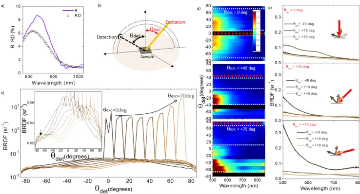
In order to better assess the composition and features of Rtot we characterized SR and RD at different
inci-dence and collection angles by measuring the spectrally- and angularly-resolved bidirectional reflectance distribution func-tion (BRDF)69,70 (see also SI Fig.SI. 8). Here the incident
beam and the detector are scanned along the same meridian and all the measured intensities are normalized to a Lamber-tian reference (the setup is shown in Fig.6b)).
Spectrally-integrated measurements show that the BRDF is composed by two distinct parts: a low-intensity, broad pedestal and a sharp peak which correspond to the scattered part RD and the specular reflection SR. The scattering RD (from 0.02 sr−1to 0.06 sr−1, Fig.4b)) is about 2-3 times lower than that of bare SiGe islands on sample II(RD from 0.06 sr−1 to 0.1 sr−1, see also Fig.SI.8 a).
In a small cone (about 10 degrees), the specular reflection is about 2 order of magnitudes larger than the scattering and stays rather constant up to ∼50 degrees, in agreement with Fig.5 b). For excitation beams at angles larger than ∼40 degrees, a slightly enhanced backscattering can be observed (highlighted by an arrow in the inset of Fig.4c)).
By taking into account the case of excitation at 10 de-grees for sample II-B, it is possible to compare this result with those obtained with the spectrophotometer for the same sample (Fig.5a), central panel) discriminating and quantify-ing SR and RD independently. Owquantify-ing to the randomized position and size of the Mie resonators on our samples, the BRDF is invariant for revolutions around the vertical direc-tion (SI Fig.SI. 8 d)). Thus, it is possible to integrate the scat-tered part over the half solid angle and the specular part over a small solid angle of about ±5 degrees around its maximum, for both angular coordinates. From this analysis, we deduce that the SR is only a few % of Rtot, confirming the result
previously shown in Fig.5a) for the integrated Rtotand RD.
Finally, the spectrally-resolved BRDF for sample II-B is measured for 3 different directions of the incident beam, θexc
= 0, +45 and +75 degrees (Fig.4d)) whereas the detection is scanned from -80 to +80 degrees. From the full datasets, we select spectra at quasi-specular, quasi-collinear, quasi-vertical direction and large angles (Fig.6e)). For all the incident an-gles, the BRDF features higher values at shorter wavelengths. For nearly-specular detection, the BRDF is larger in all the in-vestigated wavelength range and shows a marked increase at shorter wavelengths. Remarkably, for wavelengths larger than 600 nm the spectral and angular features are rather flat.
7
FIG. 6. Comparison between reflected scattering (RD) and specular reflectance (SR) for sample II-B. a) Reflected scattering RD (black triangles) and Rtot(violet line) for sample II-B at quasi-normal incidence and integrated over the half solid angle atop the sample. b) Sketch
of the experimental setup (diffusometer) used for detecting the bidirectional reflectance distribution function (BRDF). The angle of incidence of the excitation (θexc) and that of the detection (θdet) can be scanned independently over the half solid angle on the same meridian. c) BRDF
integrated from 400 nm to 800 nm for sample II-B measured for θexcfrom 0 to -70 degrees with respect to the normal to the sample surface
and θdet moving from -70 to +70. The sharp and intense peak is SR whereas the low-intensity pedestal is RD. Inset: zoom of the broad
pedestal ascribed to RD. The black arrow highlights a slight increase of the RD for incident beam at large angles. d) Full dataset of the spectrally-resolved BRDF for sample II-B for θexc= 0, +45 and +75 degrees (respectively from the top to the bottom panel). Each panel
reports the intensity of the BRDF as a color-scale as a function of wavelength and of θdet. The red dashed lines highlight θexcwhereas the
white dashed lines highlight the θdetrepresented in e). The black shaded areas hide the specular reflection. e) Spectrally-resolved BRDF for
sample II-B at θexc= 0, +45 and +75 degrees (respectively from the top to the bottom panel) for θdet= -70, +10, +70 degrees (top panel), -40,
+10, +40 (central panel) and -70, +10, +70 (bottom panel). On each panel the inset displays the excitation (red arrow) and collection (brown arrows) geometry.
IV. DISCUSSION
The extensive optical characterization and simulations per-formed on our random metasurfaces give a precise insight in the redistribution of the impinging light and its enhanced cou-pling towards the Si substrate. The analysis of the BRDF demonstrates that the large part of the reflected light is scat-tered over the half solid angle atop the sample (about 95% of Rtot) while the intensity of specular reflection is very limited
(SI Fig.SI. 3 a)).
Reflectivity and transmission measurements reveal light trapping within the substrate, pointing at the completely dif-ferent nature of our ARs with respect to conventional flat thin film coatings. In this latter case, Rtot is fully ascribed to
specular reflection, rendering the coatings less adapted to all the applications where an increased propagation path of the photons in the device is necessary (e.g. for thin-film photo-voltaic). The working principle of our samples is similar to of textured surfaces9,10with the additional feature of resonances
mediating the light coupling. In view of applications of our
AR on thin-film photovoltaic cells or light detectors, the merit of our method is to avoid a direct texturing of the Si wafer thus potentially preserving a high carrier mobility and lifetime16.
The total reflectance in our disordered samples is strongly reduced over a broad band and a broad angle, in agreement with ordered Mie resonators arrays15,16,18,21. We observe that,
for ordered arrays of Si-based dielectric particles obtained with top-down methods the best reported value of Rtot is
about 2% for above band-gap frequencies, whereas in the same spectral interval our best device reaches a value of less than 5%. However, for ordered arrays of Si-based Mie res-onators a relevant effect reducing the value of Rtot is
asso-ciated to the well-know Rayleigh anomaly15 (grating effect),
whereas in our case all the AR effect can be truly ascribed to the energy channeling mediated by the Mie resonances formed within the SiGe particles. Thus, owing to the random-ness of our samples we obtain a flatter spectral shape of Rtot
with respect to previous reports15.
In contrast with previous reports which focused only on above band-gap frequencies15,16,18,19,21, we extended this idea
to below band-gap frequencies in the near-infrared (∼1050-2500 nm) where Rtot can be as low as 7%. Moreover we
showed the possibility of tuning the minimum of Rtot both
for below- and above band-gap frequencies by adjusting the thickness of additional conformal layers deposited atop the SiGe islands. In addition, these conformal layers have the function of encapsulating the SiGe islands, rendering the metasurface more robust against mechanical damage and pro-tecting the underlying structures from humidity.
A full assessment of the performances of our spontaneously assembled structures with respect to existing examples of di-electric Mie resonators in the literature should take into ac-count the full range of frequencies addressed here, as well as the light trapping effect and the composition of light in terms of scattered reflection and specular reflection. Unfortunately, these data are not available in the literature and a comparison is not possible, which further accounts for the importance of our findings and characterizations.
In principle, this fabrication method can be performed at relatively low temperature71 (e.g. at 300◦C for thin,
amor-phous Ge layers) and it can be used on custom-made arbitrary SiO2 layers43,45 relaxing the need of a commercial UT-SOI.
Importantly, the duration of the dewetting process does not depend on the sample size, but only on the thickness of the thin Si(Ge) layer and lowering the temperature budget is pos-sible, in spite of a longer annealing time. In principle, this fab-rication method offers the possibility to implement efficient AR coatings on existing devices72(e.g. photovoltaic cells,
C-MOS and CCD cameras, Si- and Ge-based photo detectors).
V. CONCLUSIONS
We showed that joining annealing of this silicon films with epitaxial growth enable the formation of high density SiGe-based islands featuring a large vertical aspect ratio, a large spread of size with a good spatial isotropy of the particles’s size distribution. Our method represents a step forward in self-assembly of 3D structures where the size and the density of the particles are usually correlated.
The performances of our device can be adapted and im-proved employing an optimized ad hoc buried oxide43,45,64 and targeting specific wavelengths ranges with an appropri-ate choice of particles size. These possibilities bring the
addi-tional advantage of relaxing the need for expensive commer-cial UT-SOI43,45 opening up the use of this method on other
substrates (e.g. glass, Ge, SiC).
The strengths of this method are manifold: I) the duration of the process does not depend on the extension of the wafer but only on the composition and thickness of the top thin layer; II) dewetting can be exploited at relatively low temperature71and thus it can be compatible with back-end processing of C-MOS circuitry72; III) it is a lithography-free approach avoiding
mul-tiple, polluting, chemical cleaning steps as it relies only on deposition and annealing; IV) it provides efficient AR in ex-tremely broad ranges of frequencies exceeding those shown so far for similar systems15,16,18,19,21.
FUNDING INFORMATION
This project has received funding from the European Unions Horizon 2020 research and innovation programme un-der grant agreement no. 654148 Laserlab-Europe. We also acknowledge the Projects PHC MAGHREB (No. 32595SL), EMMAG-Erasmus Mundus Maghreb and Egypt, the PRCI network ULYSSES (ANR-15-CE24-0027-01) funded by the French ANR agency, the LASER-LAB Europe project ARES financed by the EU, the SATT-Sud Est Project PROMETHEUS, the A*MIDEX Project (No. ANR-11-IDEX-0001-02) funded by the Investissements d’Avenir, a French Government program managed by the French National Research Agency (ANR).
ACKNOWLEDGMENTS
The authors thank the Nanotecmat Platform of the IM2NP Institute of Marseille and the CP2M and CINaM microscopy centers of Aix-Marseille University.
†Corresponding author: [email protected]
‡ Corresponding author: [email protected] > Corresponding author: [email protected]
∗ Present address: Institut de Nanotechnologies de Lyon,
Ecole Centrale de Lyon, CNRS (UMR 5270), 69134 Ecully, France
∗∗Present address: GREMAN LAB/ST Microelectronics 16
Rue Pierre et Marie Curie 37071 Tours, France.
1
S. Chattopadhyay, Y. Huang, Y.-J. Jen, A. Ganguly, K. Chen, and L. Chen, Materials Science and Engineering: R: Reports 69, 1 (2010).
2
H. K. Raut, V. A. Ganesh, A. S. Nair, and S. Ramakrishna, Energy & Environmental Science 4, 3779 (2011).
3 M. L. Brongersma, Y. Cui, and S. Fan, Nature materials 13, 451
(2014).
4
I.-S. Yu, Y.-W. Wang, H.-E. Cheng, Z.-P. Yang, and C.-T. Lin, International Journal of Photoenergy 2013 (2013).
5
K. Kim, G. Y. Song, Y. T. Kim, J. H. Moon, and J. Heo, Surface and Coatings Technology (2017).
6
E. Yablonovitch and G. D. Cody, IEEE Transactions on Electron Devices 29, 300 (1982).
7 L. Escoubas, J. Simon, M. Loli, G. Berginc, F. Flory, and H.
Gio-vannini, Optics communications 226, 81 (2003).
8
Y.-F. Huang, S. Chattopadhyay, Y.-J. Jen, C.-Y. Peng, T.-A. Liu, Y.-K. Hsu, C.-L. Pan, H.-C. Lo, C.-H. Hsu, Y.-H. Chang, et al., Nature nanotechnology 2, 770 (2007).
9
X. Sheng, S. G. Johnson, J. Michel, and L. C. Kimerling, Optics Express 19, A841 (2011).
10
V. Ganapati, O. D. Miller, and E. Yablonovitch, IEEE Journal of Photovoltaics 4, 175 (2014).
9
11
J. Yang, F. Luo, T. S. Kao, X. Li, G. W. Ho, J. Teng, X. Luo, and M. Hong, Light: Science & Applications 3, e185 (2014).
12 H. A. Atwater and A. Polman, Nature materials 9, 205 (2010). 13
R. H. Siddique, J. Mertens, H. H¨olscher, and S. Vignolini, (2017).
14
N. Odebo Lank, R. Verre, P. Johansson, and M. Kall, Nano Letters 17, 3054 (2017).
15
P. Spinelli, M. Verschuuren, and A. Polman, Nature Communica-tions 3, 692 (2012).
16 P. Spinelli, B. Macco, M. Verschuuren, W. Kessels, and A.
Pol-man, Applied Physics Letters 102, 233902 (2013).
17
N. Fofang, T. Luk, M. Okandan, G. Nielson, and I. Brener, Optics express 21, 4774 (2013).
18 J. Proust, A.-L. Fehrembach, F. Bedu, I. Ozerov, and N. Bonod,
Scientific reports 6, 24947 (2016).
19
J. Choi, T. S. Lee, D. S. Jeong, W. S. Lee, W. M. Kim, K.-S. Lee, D. Kim, and I. Kim, Journal of Physics D: Applied Physics 49, 375108 (2016).
20
V. E. Babicheva, M. I. Petrov, K. V. Baryshnikova, and P. A. Belov, JOSA B 34, D18 (2017).
21
T. Bottein, T. Wood, T. David, J. B. Claude, L. Favre, I. Berb´ezier, A. Ronda, M. Abbarchi, and D. Grosso, Advanced Functional Materials 27 (2017).
22
J. A. Schuller, R. Zia, T. Taubner, and M. L. Brongersma, Physi-cal review letters 99, 107401 (2007).
23
Q. Zhao, J. Zhou, F. Zhang, and D. Lippens, Materials Today 12, 60 (2009).
24
A. B. Evlyukhin, C. Reinhardt, A. Seidel, B. S. Luk’yanchuk, and B. N. Chichkov, Physical Review B: Condensed Matter and Ma-terials Physics 82, 045404 (2010).
25
A. B. Evlyukhin, S. M. Novikov, U. Zywietz, R. L. Eriksen, C. Reinhardt, S. I. Bozhevolnyi, and B. N. Chichkov, Nano letters 12, 3749 (2012).
26
A. B. Evlyukhin, C. Reinhardt, E. Evlyukhin, and B. N. Chichkov, JOSA B 30, 2589 (2013).
27 D. Lin, P. Fan, E. Hasman, and M. L. Brongersma, science 345,
298 (2014).
28
S. Jahani and Z. Jacob, Nature nanotechnology 11, 23 (2016).
29
X. Li, J. Gao, L. Xue, and Y. Han, Advanced Functional Materials 20, 259 (2010).
30
K. Vynck, M. Burresi, F. Riboli, and D. S. Wiersma, Nature ma-terials 11, 1017 (2012).
31 M. Burresi, F. Pratesi, K. Vynck, M. Prasciolu, M. Tormen, and
D. S. Wiersma, Optics express 21, A268 (2013).
32
C. Rockstuhl and T. Scharf, Amorphous nanophotonics (Springer Science & Business Media, 2013).
33
H. Yasuda, R. Matsuno, N. Koito, H. Hosoda, T. Tani, and M. Naya, Applied Physics Letters 111, 231105 (2017).
34 Y. Wu, J. D. Fowlkes, and P. D. Rack, Journal of Materials
Re-search 26, 277 (2011).
35
S. Hong, T. Kang, D. Choi, Y. Choi, and L. P. Lee, ACS nano 6, 5803 (2012).
36 A. B. Tesler, B. M. Maoz, Y. Feldman, A. Vaskevich, and I.
Ru-binstein, The Journal of Physical Chemistry C 117, 11337 (2013).
37
S. Morawiec, M. J. Mendes, S. Mirabella, F. Simone, F. Priolo, and I. Crupi, Nanotechnology 24, 265601 (2013).
38
F. Bisio, R. Proietti Zaccaria, R. Moroni, G. Maidecchi, A. Al-abastri, G. Gonella, A. Giglia, L. Andolfi, S. Nannarone, L. Mat-tera, et al., ACS nano 8, 9239 (2014).
39
S. V. Makarov, V. A. Milichko, I. S. Mukhin, I. I. Shishkin, D. A. Zuev, A. M. Mozharov, A. E. Krasnok, and P. A. Belov, Laser & Photonics Reviews 10, 91 (2016).
40
R. Yu, P. Mazumder, N. F. Borrelli, A. Carrilero, D. S. Ghosh, R. A. Maniyara, D. Baker, F. J. Garcia de Abajo, and V. Pruneri, ACS Photonics 3, 1194 (2016).
41
S. Kunwar, M. Sui, Q. Zhang, P. Pandey, M.-Y. Li, and J. Lee, Nano-Micro Letters 9, 17 (2017).
42 M. Abbarchi, M. Naffouti, B. Vial, A. Benkouider, L.
Lermusi-aux, L. Favre, A. Ronda, S. Bidault, I. Berbezier, and N. Bonod, ACS nano 8, 11181 (2014).
43 M. Naffouti, T. David, A. Benkouider, L. Favre, A. Ronda,
I. Berbezier, S. Bidault, N. Bonod, and M. Abbarchi, Nanoscale 8, 7768 (2016).
44 M. Naffouti, T. David, A. Benkouider, L. Favre, M. Cabie,
A. Ronda, I. Berbezier, and M. Abbarchi, Nanotechnology 27, 305602 (2016).
45
T. Wood, M. Naffouti, J. Berthelot, T. David, J.-B. Claude, L. Metayer, A. Delobbe, L. Favre, A. Ronda, I. Berbezier, N. Bonod, and M. Abbarchi, ACS Photonics 4, 873 (2017).
46
M. Naffouti, R. Backofen, M. Salvalaglio, T. Bottein, M. Lodari, A. Voigt, T. David, A. Benkouider, I. Fraj, L. Favre, et al., Science Advances 3, eaao1472 (2017).
47
D. Srolovitz and S. Safran, Journal of Applied Physics 60, 247 (1986).
48
D. Srolovitz and S. Safran, Journal of applied physics 60, 255 (1986).
49 E. Jiran and C. Thompson, Journal of electronic materials 19,
1153 (1990).
50
D. T. Danielson, D. K. Sparacin, J. Michel, and L. C. Kimerling, Journal of applied physics 100, 083507 (2006).
51 C. M. M¨uller and R. Spolenak, Acta materialia 58, 6035 (2010). 52
F. Cheynis, E. Bussmann, F. Leroy, T. Passanante, and P. M¨uller, Physical Review B 84, 245439 (2011).
53 C. V. Thompson, Annual Review of Materials Research 42, 399
(2012).
54
F. Leroy, F. Cheynis, T. Passanante, and P. M¨uller, Physical Re-view B 85, 195414 (2012).
55
G. Hyun Kim, R. V. Zucker, J. Ye, W. Craig Carter, and C. V. Thompson, Journal of Applied Physics 113, 043512 (2013).
56 R. V. Zucker, G. H. Kim, W. C. Carter, and C. V. Thompson,
Comptes Rendus Physique 14, 564 (2013).
57
G. Boussinot and E. A. Brener, Physical Review E 92, 032408 (2015).
58 R. V. Zucker, G. H. Kim, J. Ye, W. C. Carter, and C. V. Thompson,
Journal of Applied Physics 119, 125306 (2016).
59
M. Aouassa, I. Berbezier, L. Favre, A. Ronda, M. Bollani, R. Sor-dan, A. Delobbe, and P. Sudraud, Applied Physics Letters 101, 013117 (2012).
60
E. Sutter and P. Sutter, Nanotechnology 17, 3724 (2006).
61 M. Naffouti, T. David, A. Benkouider, L. Favre, A. Delobbe,
A. Ronda, I. Berbezier, and M. Abbarchi, Small 12, 6115 (2016).
62
M. Aouassa, L. Favre, A. Ronda, H. Maaref, and I. Berbezier, New Journal of Physics 14, 063038 (2012).
63
P. Zhang, B. Yang, P. Rugheimer, M. Roberts, D. Savage, F. Liu, and M. Lagally, Journal of Physics D: Applied Physics 42, 175309 (2009).
64 J. van de Groep and A. Polman, Optics express 21, 26285 (2013). 65
H. Kallel, A. Chehaidar, A. Arbouet, and V. Paillard, Journal of Applied Physics 114, 224312 (2013).
66 A. Chehaidar and H. Jdidi, International Journal of
Nanotechnol-ogy 12, 663 (2015).
67
H. Kallel, A. Arbouet, G. BenAssayag, A. Chehaidar, A. Poti´e, B. Salem, T. Baron, and V. Paillard, Physical Review B 86, 085318 (2012).
68
X. Zhu, W. Yan, U. Levy, N. A. Mortensen, and A. Kristensen, Science Advances 3, e1602487 (2017).
69
W. Matusik, H. Pfister, M. Brand, and L. McMillan, (2003).
70
T. A. Germer, J. C. Stover, and S. Schroeder, Spectrophotome-try: Accurate Measurements of the Optical Properties of Materials
(2014). 71 Y. Wakayama, T. Tagami, and S.-i. Tanaka, Thin Solid Films 350, 300 (1999).
72 Y. H. D. Lee and M. Lipson, IEEE Journal of Selected Topics in