HAL Id: tel-01278532
https://tel.archives-ouvertes.fr/tel-01278532
Submitted on 24 Feb 2016
HAL is a multi-disciplinary open access
archive for the deposit and dissemination of sci-entific research documents, whether they are pub-lished or not. The documents may come from teaching and research institutions in France or abroad, or from public or private research centers.
L’archive ouverte pluridisciplinaire HAL, est destinée au dépôt et à la diffusion de documents scientifiques de niveau recherche, publiés ou non, émanant des établissements d’enseignement et de recherche français ou étrangers, des laboratoires publics ou privés.
On design concept for full-duplex based flexible radio
transceivers
Zhaowu Zhan
To cite this version:
Zhaowu Zhan. On design concept for full-duplex based flexible radio transceivers. Networking and Internet Architecture [cs.NI]. INSA de Lyon, 2014. English. �NNT : 2014ISAL0142�. �tel-01278532�
Number of Order 2014-ISAL-0142 Year 2014
THESIS
ON DESIGN CONCEPT FOR FULL-DUPLEX BASED
FLEXIBLE RADIO TRANSCEIVERS
defended at
L’INSTITUT NATIONAL DESSCIENCESAPPLIQUÉES DELYON
for the degree of
Doctor of Philosophy
École Doctorale :
ÉLECTRONIQUE, ÉLECTROTECHNIQUE ET AUTOMATIQUESpécialité :
STIC SANTÉBy
Zhaowu ZHAN
Defense on 16 December 2014 THESIS COMMITTEE
Andreas BURG EPFL, Ass. Professor Reviewer
Ioannis KRIKIDIS University of Cyprus, Ass. Professor Reviewer
Jean-François DIOURIS Polytech Nantes, Professeur Reviewer
Patrick ROSSON Ingénieur R&D, CEA-Leti Grenoble Examiner
Jean-Marie GORCE INSA de Lyon, Professeur Examiner
Guillaume VILLEMAUD INSA de Lyon, Maître de Conférences, HDR Director
This thesis was prepared at CITI Laboratory, INSA de Lyon - INRIA Rhône-Alpes
Abstract
The wireless medium is a shared and limited resource. Current wireless standards always share the medium with Half-Duplex principle: the transmission and recep-tion of signals are done in two separate time slots or two different frequency bands. Besides, the transceiver can only transmit and receive one signal at a time.
This dissertation takes an alternate approach: Instead of sharing the medium with Half-Duplex principle, the entire licensed frequency band is shared for simultaneous transmission and reception, which we call Full-Duplex. Besides, the design concept for a wideband flexible radio transceiver can process two different types of signals at a time.
To reach this goal, we propose to use an active analog radio frequency (RF) self-interference cancellation (AARFSIC) method or a combination scheme of the AARF-SICand active digital self-interference cancellation in time domain (ADSICT) to cancel the strong self-interference (SI) induced by the Full-Duplex principle. Based on the Full-Duplex radio, we propose a flexible Full-Duplex Dual-Band (FDDB) OFDM radio transceiver by combining the Dual-Band RF front-end.
Building on these, we make three main contributions: We present an active self-interference cancellation (ASIC) scheme, which can cancel both the strong one-path and multi-path SI completely, based on the combination of the AARFSIC and DSICT. Next, we introduce the design and evaluation of a Full-Duplex OFDM radio, includ-ing analysis and qualification of the impact of the thermal noise and phase noise on the system performance. Finally, we develop an FDDB OFDM radio that can work on two separate spectrum fragments. In order to eliminate the impact of the I/Q imbal-ance on the FDDB radio, a simple but practical digital I/Q imbalimbal-ance estimation and compensation method is presented. The system level simulation conducted with ADS and Matlab software shows that this method can efficiently compensate both high and low I/Q imbalance.
Key-words : Full-Duplex, Self-interference cancellation, OFDM, Full-Duplex
Résumé
Le medium sans fil est une ressource partagée et limitée. Les normes sans fil actuelles partagent toujours le principe de partage du medium Half-Duplex: la trans-mission et la réception de signaux sont effectuées dans deux intervalles de temps dis-tincts ou deux bandes de fréquences différentes. En outre, l’émetteur-récepteur ne peut émettre et recevoir qu’un signal à la fois.
Cette thèse suit une autre approche: au lieu de partager le support avec le principe de Half-Duplex, toute la bande de fréquence autorisée est partagé pour la transmission et la réception simultanée, approche qui est appelée Full-Duplex. Dès lors, on peut concevoir une architecture d’un émetteur-récepteur radio flexible à large bande pour traiter deux types de signaux différents à la fois.
Pour approcher cet objectif, nous utilisons une méthode de suppression active analogique de l’auto-interférence (AARFSIC) et l’annulation active numérique d’auto-interférence dans le domaine temporel (ADSICT) pour annuler la forte auto-d’auto-interférence (SI) induite par le principe Full-Duplex. Basé sur la radio Full-Duplex, nous proposons un système flexible Dual-Band (FDDB) émetteur-récepteur radio OFDM Full-Duplex en la combinant avec un front-end RF double bande.
S’appuyant sur ces principes, nous exposons trois contributions principales: Nous présentons une technique d’annulation analogique de l’auto-interférence (ASIC), qui peut annuler complètement l’auto-interférence à trajet direct ou multi-trajets, basée sur la combinaison des méthodes AARFSIC et DSICT. Ensuite, nous présentons la con-ception et l’évaluation d’une radio OFDM Full-Duplex, y compris l’analyse et la qual-ification de l’impact du bruit thermique et du bruit de phase sur les performances du système. Enfin, nous développons une radio dual-bande FDDB OFDM qui peut fonc-tionner sur deux fragments de spectre séparés. Afin d’éliminer l’impact du déséquili-bre I/Q sur la radio FDDB, une méthode d’estimation des déséquilidéséquili-bres I/Q et de compensation, simple mais efficace, est présentée. La simulation au niveau système menée avec ADS et Matlab montre que cette méthode peut effectivement compenser des déséquilibres I/Q aussi bien élevés que faibles.
Mots-clés: Full-Duplex, annulation auto-interférence, OFDM, Full-Duplex Dual-Bande,
To my beloved parents and sister.
To my beloved wife.
Acknowledgements
The research work for this PhD dissertation was carried out during the years 2011-2014 at the CITI Research Laboratory (INSA Lyon - INRIA), Lyon. This place has provided me good conditions and great atmospheres for scientific research. Moreover, the UT-INSA project financially supported by the China Scholarship Council (CSC) gives me this opportunity to study in INSA Lyon, France.
Furthermore, I would like to express my sincerely appreciates to many peoples. First of all, I would like to thank Dr. Guillaume Villemaud. My experience was en-riched tremendously by having him as my advisor. From my first year at the CITI Lab, despite my unfamiliarity with scientific research and pool oral english, he always discussed with me with great patience. He teaches me how to do research, gives me valuable advice and provides me encouragement and support, which led to the valu-able results of this dissertation.
I am very grateful to Prof. Jean-Marie Gorce, who is my dissertation director in the first two and half years. Although we had very limited several talks, his passions on the scientific research greatly impressed me. Besides, he gave me some excellent valuable advices on my future professional career.
In addition, I would like to thank Prof. Andrea Burg, Prof. Ioannis Krikidis and Prof. Jean-François Diouris for making effort to read and review this dissertation, as well as thank Patrick Rosson and Prof. Jean-Marie Gorce for accepting to examine this dissertation.
Finally, I would like to take this opportunity to thank my dear friends and col-leagues for their kindness and help all these years.
Lyon, Oct. 21. 2014 Zhaowu Zhan
Contents
Abstract iii Résumé v Acknowledgements ix Acronyms 1 1 Introduction 31.1 Flexible Radio Transceivers . . . 3
1.1.1 Overview . . . 3
1.1.2 Cognitive Radios . . . 4
1.1.3 Multimode Radios . . . 5
1.1.4 Full-Duplex Radios . . . 6
1.2 Context and Motivation . . . 6
1.2.1 Digital Baseband Communications. . . 6
1.2.2 Transceiver RF Front-End . . . 17
1.3 Contribution and Outline . . . 19
1.3.1 Contribution . . . 19
1.3.2 Thesis Outline. . . 19
1.4 Related Publications . . . 21
I
Self-Interference Cancellation in Full-Duplex Wireless
23
2 State-of-the-Art of the Self-Interference Cancellation 25 2.1 Antenna Cancellation . . . 262.1.1 Antenna Cancellation based on λ/2 Spacing . . . 26
2.1.2 Antenna Cancellation based on Symmetry . . . 27
2.3 Active Self-Interference Cancellation . . . 30
2.3.1 Active Analog Self-Interference Cancellation . . . 31
2.3.2 Active Digital Self-Interference Cancellation . . . 35
2.4 Key Factors Limiting the Self-Interference Cancellation . . . 37
2.4.1 RF Impairments. . . 38
2.4.2 Multiple Paths of the Self-Interference Channel . . . 40
2.5 Conclusion and Discussion . . . 41
3 Self-Interference Cancellation for Full-Duplex OFDM Wireless 43 3.1 AARFSIC for Full-Duplex OFDM Wireless . . . 43
3.1.1 AARFSIC for One-Path Full-Duplex OFDM Wireless . . . 45
3.1.2 AARFSIC for Multi-Path Full-Duplex OFDM Wireless . . . 47
3.1.3 Characters of the Residual Self-Interference . . . 50
3.2 Digital SIC in Time Domain . . . 52
3.3 Conclusion and Discussion . . . 54
II
Full-Duplex OFDM Wireless Radios
55
4 Full-Duplex OFDM Radio Design 57 4.1 State-of-the-Art of the Full-Duplex Prototype . . . 584.2 General System Model of Full-Duplex OFDM Wireless . . . 59
4.2.1 Signal Model . . . 60
4.2.2 Channel Model . . . 61
4.2.3 Channel Estimation . . . 61
4.3 Full-Duplex OFDM Wireless with One-Path SI Channel . . . 63
4.3.1 Active Analog RF Self-Interference Cancellation . . . 63
4.3.2 Effect and Mitigation of RF Impairments . . . 67
4.4 Full-Duplex OFDM Wireless with Multi-Path SI Channel . . . 74
4.4.1 Active Analog RF Self-Interference Cancellation . . . 74
4.4.2 Digital Self-Interference Cancellation in Time Domain. . . 76
4.5 Residual Self-Interference . . . 81
4.5.1 Without RF Impairments . . . 82
4.5.2 With RF Impairments . . . 82
4.6 Full-Duplex OFDM Radio Transceiver Design. . . 82
III
Full-Duplex Dual-Band Wireless Radios
87
5 Full-Duplex Dual-Band OFDM Radio Transceiver 89
5.1 Introduction . . . 90
5.2 Related Works . . . 91
5.2.1 State-of-the-Art of the SIC for Full-Duplex Wireless . . . 91
5.2.2 Related Works on I/Q Imbalance Estimation and Compensation 92 5.3 Full-Duplex Dual-Band Radio . . . 93
5.3.1 Full-Duplex Radio . . . 94
5.3.2 Dual-Band RF Front-End . . . 96
5.4 Impact of I/Q Imbalance on the Full-Duplex Dual-Band OFDM Radios . 98 5.5 Digital Estimation and Compensation of I/Q Imbalance . . . 100
5.5.1 Digital Estimation of I/Q Imbalance . . . 100
5.5.2 Digital Compensation of I/Q Imbalance. . . 106
5.6 Full-Duplex Dual-Band OFDM Radio Transceiver . . . 107
5.7 Performance Evaluation and Discussion . . . 108
5.7.1 Performance Evaluation . . . 109
5.7.2 Discussion . . . 111
5.8 Conclusion . . . 113
IV
Conclusion and Future Outlook
115
6 Conclusion and Future Outlook 117 6.1 Conclusion . . . 1176.2 Future Outlook . . . 118
V
References
121
Bibliography 123
List of Tables
List of Figures
1.1 Block diagram of a general cognitive radio transceiver. . . 4
1.2 Block diagram of an adaptive multimode receiver. . . 5
1.3 Block diagram of a general wireless communication system. . . 6
1.4 Basic diagram of an OFDM baseband transmitter. . . 7
1.5 Basic block diagram of an OFDM baseband receiver. . . 9
1.6 Basic block diagram of a MIMO baseband transceiver. . . 12
1.7 Equivalent parallel SISO channel of MIMO-SVD. . . 14
1.8 Structure of a linear pre-coder.. . . 15
1.9 Illustration of a MIMO-OFDM transmitter. . . 16
1.10 Illustration of a MIMO-OFDM receiver. . . 17
1.11 Simplified architecture of a direct conversion transmitter and receiver RF front-end. . . 18
1.12 Simplified architecture of a superheterodyne RF front-end. . . 18
2.1 The block diagram of the SAC.. . . 26
2.2 Block diagram of the Transmit Antenna Cancellation. . . 27
2.3 Block diagram of the Receive Antenna Cancellation. . . 28
2.4 Block diagram of the NEC-PAC. . . 29
2.5 Classical radio receiver with possible SIC placements. . . 30
2.6 Simplified block diagram of Stanford AARFSIC. . . 31
2.7 Simplified block diagram of Rice AARFSIC. . . 32
2.8 Illustration of the digitization of the mixed signals including the SI and the desired signal by ADC.. . . 34
2.9 Simplified block diagram of AABBSIC. . . 35
2.10 General block diagram of ADSIC. . . 35
2.11 Perfectly synchronized OFDM system can be viewed as a set of parallel Gaussian sub-carrier channels. . . 37
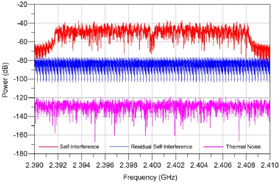
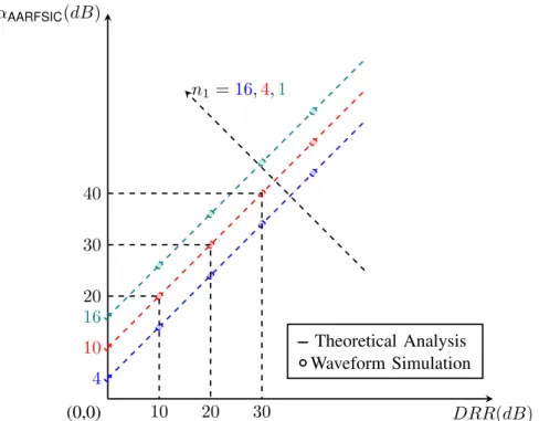
3.2 When the Full-Duplex OFDM wireless with multipath (here 2 paths SI wireless channel is considered, the second path has 50ns time delay and 20dB attenuation compared to the first path) SI channel, the AARFSIC has a very limited capability of SIC. As it is shown, the power of the strong SI at the antenna of the receiver is 80dB higher than the thermal noise. The AARFSIC can only achieve around 36dB SIC. Therefore, there is still 44dB residual SI. . . 48
3.3 The amount of SIC by AARFSIC when the SI channel consists of a direct path and one reflecting path. . . 51
3.4 The block diagram of DSICT. . . 52
4.1 Block diagram of a Full-Duplex wireless transmission.. . . 60
4.2 One-path SI channel:Comparison of the spectrum power (dBm) of the
SI before and after the AARFSIC with different INR . (ADS simulation) . 66
4.3 One-path SI channel: The BER performance comparison of the
Full-Duplex OFDM wireless with different INR. . . 67
4.4 NMSE of the self-interference channel estimation vs. INR. . . 69
4.5 The structure of the redesigned data packet. . . 70
4.6 The BER comparison of the Full-Duplex wireless for different INRs. . . . 70
4.7 The BER of the Full-Duplex wireless for INR=5dB with different α. . . . 71
4.8 The analysis signal model of AARFSIC for the Full-Duplex wireless with phase noise. . . 72
4.9 The BER performance comparison of the Full-Duplex 802.11g with dif-ferent phase noise level. . . 73
4.10 Magnitude measurement of the received signals before and after the AARFSIC. The received signals consist of the direct-path signal and an-other reflecting-path signal when the two-path SI channel is used here. The reflecting path has 50ns delay and 20dB attenuation compared to the direct path. (Note: For the wireless system with 20MHz bandwidth, 50nsmeans one sampled point. Hence, 50ns delay in continuous time domain represents one sampled point delay in discrete time domain.). . 75
4.11 Multi-path SI channel: The BER performance of the Full-Duplex IEEE 802.11g with the AARFSIC for multi-path SIC. When Eb/N0 ≤ 16dB, the
BER performance is determined by the receiver thermal noise. How-ever, when Eb/N0 > 16dB, the BER performance begin to be mainly
4.12 The residual peaks after the AARFSIC. In this waveform simulation, the number of the paths of the SI channel is Nsip = 3. The second path
has 20dB attenuation and 50ns delay compared to the direct path. The third path has 40dB attenuation and 150ns delay compared to the di-rect path. Therefore, there are three non-zeros points. The first point is caused by the combination of the second path and the third path. The second point and the third point are caused by the third path. . . 77
4.13 General structure of the mth
0 generated OFDM symbol, xTm0(n), n ∈ [1, N +
NCP], in IEEE 802.11g. . . 78
4.14 General structure of the received OFDM symbol in IEEE 802.11g. . . 78
4.15 The structure of the crafted cancellation OFDM symbol. . . 79
4.16 Multi-path SI channel: The comparison of the BER performance be-tween the Full-Duplex IEEE 802.11g with perfect channel estimation and the standard IEEE 802.11g system. . . 80
4.17 Multi-path SI channel: The comparison of the BER performance be-tween the Full-Duplex IEEE 802.11g with real channel estimation and the standard IEEE 802.11g system. . . 81
4.18 Architecture of Full-Duplex OFDM radio node.. . . 83
5.1 One application scenario of FDDB radio.. . . 90
5.2 Block diagram of a general Full-Duplex Dual-Band wireless radios. . . . 93
5.3 Design in details of the Full-Duplex Dual-Band wireless radios. . . 94
5.4 Architecture of self-interference cancellation for in-band two-antenna Full-Duplex wireless. . . 95
5.5 The frame structure for the in-band two-antenna Full-Duplex IEEE 802.11g. 96
5.6 Architecture of the Dual-Band RF front-end. . . 96
5.7 Architecture of Dual-Band RF front-end with I/Q imbalance.. . . 99
5.8 The estimated magnitude of each subcarrier channel of the
over-the-air SI channel with or without I/Q Imbalance. Without I/Q imbalance,
the over-the-air SI channel is almost a frequency flat fading channel, while the SI channel will be a frequency selective fading channel when I/Q imbalance (∆A = 0.2, ∆φ = 10o) exists in the FDDB radio front-end. 102
5.9 Compensation block for the I/Q imbalance. . . 107
5.10 Full-Duplex Dual-Band OFDM radio transceiver with I/Q imbalance compensation. . . 108
5.11 The BER of Full-Duplex Dual-Band 802.11g wireless system, with ideal I/Q. . . 110
5.12 The BER of Full-Duplex Dual-Band 802.11g wireless system, with I/Q imbalance ( ∆A = 0.2, ∆φ = 10o). . . 111
5.13 The BER of Full-Duplex Dual-Band 802.11g wireless system, with I/Q imbalance (∆A = 0.1, ∆φ = 5o). . . . 112
5.14 The BER of Full-Duplex Dual-Band 802.11g wireless system, with I/Q imbalance (∆A = 0.05, ∆φ = 1o). . . 112
Acronyms
List of Acronyms
AABBSIC Active Analog BaseBand Self-Interference Cancellation.
AARFSIC Active Analog Radio Frequency Self-Interference Cancellation. ADSIC Active Digital Self-Interference Cancellation.
ASIC Active Self-Interference Cancellation.
AWGN Additive White Gaussian Noise.
BER Bit Error Rate.
CSI Channel State Information.
DFT Discrete Fourier Transform.
DRR Direct-path to Reflect-path Ratio.
DSIC Digital Self-Interference Cancellation.
DSICF Digital Self-Interference Cancellation in Frequency domain. DSICT Digital Self-Interference Cancellation in Time domain.
FDDB Full-Duplex Dual-Band.
GI Guard Interval.
IDFT Inverse Discrete Fourier Transform.
INR self-Interference-to-Noise Ratio.
LoS Line-of-Sight.
LNA Low Noise Amplifier.
LS Least Square.
MIMO Multiple-Input Multiple-Output.
MSE Mean Square Error.
NLoS Non-Line-of-Sight.
NMSE Normalized Mean Square Error.
OFDM Orthogonal Frequency Division Multiplexing.
PA Power Amplifier.
PSIS Passive Self-Interference Suppression.
SI Self-Interference.
1
Introduction
The radio transceiver is concerned with the transmission and reception of the digital data symbols across the wireless channel via an RF front-end. Therefore, the radio transceiver design should include the baseband system design and RF front-end de-sign. For the flexible radio transceiver design, the radio front-end should be capable of processing different RF signals and the baseband system should have the abilities to separate and recover different data symbols belong to different demands.
1.1
Flexible Radio Transceivers
1.1.1
Overview
It has been more than one century sine the invention of the wireless radio transmis-sion using electromagnetic wave. In 1893, Nikolai Tesla demonstrated the wireless radio communications in St. Louis, which implied the beginning of the radio develop-ment. From the first telegraph to the first wireline telephone and to the first wireless telephone, and even to the modern digital cellular mobile phones, the way of infor-mation transmissions and radio applications have been experiencing great changes. The wireless radios enable the information to be transfered far and wide. Wireless ra-dio terminals are increasingly pervasive in our everyday life. Initial wireless systems
4 Flexible Radio Transceivers
were designed and developed to support only voice signal. However, current and fu-ture wireless systems will more focus on the high data rate transmissions due to the extensive deployment of multimedia applications and looking forward to the inter-net by people. Therefore, current and future wireless inter-networks need to be designed and developed not only to support voice but also to support the data and multimedia applications.
There are several broadband wireless standards currently, such as the third gener-ation (3G), the fourth genergener-ation (4G) and wireless fidelity (WiFi) and so on, which support relative high throughput compared to the first generation analog wireless communication and the second generation (2G). However, all these technologies, even the latest 4G, can not meet the requirement of the high data rate to be faced in the fu-ture. Besides, one radio terminal should accommodate different wireless technologies to be compatible with different wireless standards. Therefore, the designs of radio transceivers are challenged by the high flexibility and reconfigurability constraints.
1.1.2
Cognitive Radios
In 1998, Joseph Mitola III proposed the concept of cognitive radio which was defined as an intelligent radio system [82]. Cognitive radios are required to have the both abil-ities to sense the surrounding spectral environment and flexibly adapt its transceiver parameters to optimize the radio link. However, finding a suitable radio front-end to realize a flexible wideband and agile radio transceiver is always a big challenge. Cog-nitive radio requires a novel radio frequency (RF) transceiver architecture to provide cognitive capability and reconfigurability [9]. A cognitive radio transceiver is com-posed of two main components: RF front-end and baseband processing system. In the RF front-end, the received signal is amplified, mixed and analog-to-digital con-verted (ADC). While in the baseband, the signal is modulated or demodulated. Each component should be reconfigured via control bus to adapt to the time-varying radio environment as shown in Fig.1.1.
u1 u2 d1 d2 Radio Frequency Analog-to-Digital /Digital-to-Analog Converter Digital Baseband System Rx Tx
Control Bus (Reconfiguration) RF Front-End
(wideband sensing)
Figure 1.1: Block diagram of a general cognitive radio transceiver.
Cette thèse est accessible à l'adresse : http://theses.insa-lyon.fr/publication/2014ISAL0142/these.pdf © [Z. Zhan], [2014], INSA de Lyon, tous droits réservés
Introduction 5
The cognitive radio transceiver should be equipped with a wideband RF front-end that is capable of sensing simultaneously over a wide frequency range. This capability is mainly related to the RF hardware, such as wideband antenna, power amplifier and adaptive filter [9]. A cognitive radio transceiver will receive signals from various ra-dio terminals operating on different spectrum channels and at different power levels. Therefore, the RF front-end of a cognitive radio should have the capability of detect-ing a weak signal in a large dynamic range of frequency bands. This is a big challenge behind the design of the cognitive radio transceivers [29].
1.1.3
Multimode Radios
Various services demand a mobile terminal to support different wireless communica-tion standards, so the integrated multi-standard wireless devices is required. In cur-rent wireless systems equipped with multi-standard functionality, the transceivers are mostly implemented by using separate RF front-end for each individual standard and sharing partially the analog baseband circuitry with the aid of a number of additional switchers. Although this approach could enable a radio terminal to accommodate various wireless standards, the increase in the hardware required to implement such a multi-standard radio transceiver increases the circuitry area, the cost as well as may increase the power consumption compared to the conventional single-standard radio transceiver implementation [53].
A radio which is multimode/multiband should work in multiple bands with few or no modifications. The block diagram of a multimode receiver [53] with an adaptive RF front-end, adaptive analog baseband circuitry and adaptive digital signal process-ing is illustrated in Fig.1.2.
u1 u2 d1 d2 Radio Frequency Analog-to-Digital /Digital-to-Analog Converter Digital Baseband System Rx
Control Bus Reconfiguration RF Front-End (wideband sensing) LNA LNA Quadrature Generation VCO LNA cos(fc) sin(fc) VGA VGA ADC ADC Adaptive Digital Signal Processing Adaptive Analog RF Front-End Adaptive Analog Baseband
Figure 1.2: Block diagram of an adaptive multimode receiver.
Although this kind of multimode radio receiver can accommodate various wire-less standards, it just can process one signal at a time.
Cette thèse est accessible à l'adresse : http://theses.insa-lyon.fr/publication/2014ISAL0142/these.pdf © [Z. Zhan], [2014], INSA de Lyon, tous droits réservés
6 Context and Motivation
1.1.4
Full-Duplex Radios
Full-Duplex is defined as a radio which can simultaneously transmit and receive sig-nals over the same frequency band. Such a capability can be exploited to offer high efficiency of spectrum utilization, more efficient relaying, as well as more flexible medium access. Hence, Full-Duplex radio could show great potentialities for the fu-ture flexible radio transceiver design. Half-Duplex (i.e. FDD and TDD) is not only inefficient in the radio resource utilization but also in medium access. FDD, requiring paired-spectrum for uplink and downlink transmission, can not realize the flexible spectrum access. TDD, requiring different time slots for uplink and downlink con-nection, is inefficient in real time communications. While in the Full-Duplex mode meaning that one spectrum fragment can be used for both transmission and recep-tion at a time, both of the demands of high efficiency of radio resource utilizarecep-tion and flexible access to medium can be met.
Besides, spectrum fragmentation will be compounded in the future 5G wireless network driven by the scarcity of spectrum [47], which can be enhanced by the Full-Duplex technique.
1.2
Context and Motivation
The physical layer is concerned with the transmission and the reception of digital in-formation over the wireless channel via an RF front-end. Therefore, a general wireless communication system consists of a transmitter, a wireless channel and a receiver. The transmitter includes digital baseband system and transmitter RF front-end. The re-ceiver includes rere-ceiver RF front-end and the correspondent digital baseband rere-ceiver system. Therefore, a general wireless system can be described as Fig.1.3
-Xm[k]H[k] iFFT Modulation Xm[k] DAC Front-EndTx RF Rx RF Front-End Rx Combiner iFFT Modulation DAC Tx RF Front-End ADC FFT Modulation Self-Interference Channel Estimation -H[k] Tx Cancellation Path Digital Baseband Transmitter System Xm[k] DAC Front-EndTx RF Tx Rx RF Front-End Rx
ADC Digital Baseband Receiver System Ym[k] Digital Domain Analog Domain Analog Domain Digital Domain
x(t)*h(t)+n=y(t)
Figure 1.3: Block diagram of a general wireless communication system.
1.2.1
Digital Baseband Communications
The wireless revolution has resulted in ever increasing demands on high data rate over limited wireless spectrum, putting much more requirement of higher spectral
Introduction 7
efficiency on the wireless systems. Therefore, the telecommunication engineers are always exploring the advanced physical layer techniques to approach this goal.
Multicarrier System
Orthogonal Frequency Division Multiplexing (OFDM) utilizes a large number of parallel and orthogonal narrow-band sub-carriers instead of a single wide-band car-rier to transmit and receive informations. In details, OFDM divides a wideband quency selective fading channel into an set of equivalent parallel narrowband fre-quency flat fading sub-channels. This division is achieved by splitting the input high-data stream into a number of substreams that are transmitted in parallel over the or-thogonal sub-carriers. The sub-carriers are designed in order to have a minimum fre-quency space to maintain the orthogonality between different sub-channels and the adjacent signal spectra corresponding to different sub-carriers overlap with each other in frequency. Therefore, the available bandwidth is used more efficiently compared to a traditional single carrier system.
The basic diagram of a baseband OFDM transmitter is as shown in Fig.1.4.
Mapper S/P 2 / ) cos(0t 0 0 0 a jb s 0 a 0 b 2 / ) cos(1t 1 1 1 a jb s 1 a 1 b 2 / ) cos(N1t 1 1 1 N N N a jb s 1 N a 1 N b CP CP
+
Window DAC RF Front-End Message Bits Scrambling & Channel Coding & Interleaving Coded Bits Symbols I & Q Samples Baseband SignalFigure 1.4: Basic diagram of an OFDM baseband transmitter.
At the transmitter, a message is first scrambled via multiplying it with a pseudo-random bit sequence in order to eliminate the unwanted regularity in the message that may confuse some PHY algorithm. Then, some form of forward error correction (FEC) is added to the scrambled message to protect against the channel-induced distortion. In order to make the FEC work more effectively, the transmitter optionally interleaves
8 Context and Motivation
the coded bits so that the adjacent coded bits will temporally non-adjacent to against the deep channel fading. Next, the transmitter uses the modulator or mapper to take groups of coded bits and maps them into complex baseband symbols for transmission by the RF front-end. The complex symbol X[k] = ak+ bkproduced by the modulator will be converted into time-domain samples by using the Inverse Discrete Fourier Transform (IDFT), because the transmission hardwares operate only on time samples. The output of the IDFT are complex time-domain samples with real (I) and imaginary (Q) components. The I and Q components represent the two orthogonal dimensions along which informations could be transmitted via using electromagnetic waves.
Let {X[0], X[1], ..., X[N − 1]} be a block of N data symbols after the serial-to-parallel conversion. The kth data symbol will be carried by the kthsub-carrier. Then, the baseband time domain complex samples x(n) can be obtained by IDFT of the sym-bol block as x(n) = 1 N N −1 X k=0 X[k]eωkn ωk=2πkN = 1 N N −1 X k=0 X[k]e2πknN , n = 0, 1, ..., N − 1, (1.1)
where the imaginary unit =√−1 and ωk= 2πkN .
After that, a guard interval (GI) is introduced to preserve the orthogonality of the sub-carriers and the independence of the adjacent OFDM symbols when the OFDM signal experiences a multi-path time-dispersive radio channel. The guard interval, usually using a cyclic prefix (CP), is the copy of the last part of the OFDM symbol. The duration of the GI, Tguardis chosen larger than the maximum excess delay of the
multi-path radio channel. Because of the CP, the linear convolution of the transmitted symbols with the wireless channel is transformed to a circular convolution. Window-ing is a well-known technique to reduce the power level of the side-lobes and thereby reduce the signal power out of band. In an OFDM system, the applied window must not influence the signal during its effective period [84].
These baseband I and Q samples obtained from above are then up-converted to the desired transmission frequency signal and transmitted over the air as analog waves by the RF front-end. The to be transmitted RF signal over the air could be expressed as
xRF(t) = x(t)e2πfct (1.2)
where x(t) denotes the continuous baseband time-domain signal, fc denotes the de-sired center carrier frequency. Over the multi-path fading channel h(t), the received
Introduction 9
RF signal can be expressed as
yRF(t) = x(t)e2πfct∗ h(t) + wRF(t) (1.3)
where wRF(t)denotes the receiver thermal noise in the RF analog domain.
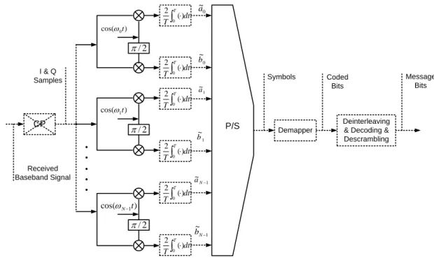
The basic block diagram of a baseband OFDM receiver is as shown in Fig.1.5.
Mapper 2 / ) cos(0t 2 / ) cos(1t 2 / ) cos(N1t CP Bits CP dt T T 0() 2 dt T T 0() 2 dt T T 0() 2 dt T T 0() 2 dt T T 0() 2 dt T T 0() 2 0 ~ a 0 ~ b 1 ~ a 1 ~ N a 1 ~ N b 1 ~ b Demapper
P/S Deinterleaving & Decoding &
Descrambling Received
Baseband Signal I & Q
Samples Symbols Coded Bits
Message Bits
Figure 1.5: Basic block diagram of an OFDM baseband receiver.
At the receiver side, the RF signals received by the receive antenna is first down-converted to baseband continuous domain signal. Then, this continuous time-domain signal will be digitized via analog-to-digital converter (ADC). The obtained discrete time-domain signal will be further processed by the OFDM baseband receiver. If the transceiver RF front-ends are assumed ideal, the received baseband equiva-lent signal y(t) could be expressed as
y(t) = x(t) ∗ h(t) + w(t) (1.4) where w(t) denotes the receiver thermal noise in the continuous time domain. The demodulation of the OFDM signal should be performed by a bank of filters which are “matched” to the effective part of the OFDM symbol. Exact formulation of such a
10 Context and Motivation
bank of matched filters is as
Y [k] = 2 T Z T 0 y(t)e−ωktdt = 2 T Z T 0 y(t)e−2πktN dt (1.5) Here, we obtained the complex symbol Y [k] =aek+ ebkwhich is correspondent to the
transmitted complex symbol X[k] = ak+ bk.
In fact, because of the CP, the received equivalent baseband discrete time-domain signal can be represented in another way by
y(n) = x(n) ~ h(n) + w(n) (1.6) where ~ denotes the circular convolution and w(n) is the receiver thermal noise. After removing the CP, the received discrete time-domain signal is
y(n) = N X k=0 X[k]H[k]e2πknN + w(n) (1.7) where H[k] = PN n=0h(n)e− 2πkn
N is the frequency domain expression of the wireless channel. Then, we can recover the frequency domain symbols by demodulating the received time domain OFDM symbol as
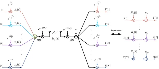
Y [k] = N X n=0 y(n)e−2πknN = X[k]H[k] + W [k] (1.8) Eq. (1.8) shows that OFDM transmission over a wireless frequency selective channel, as in (1.6), is equivalent to symbol transmission over N parallel sub-carrier channels.
If the transfer function of the kth sub-carrier channel can be obtained as H[k]e , the transmitted complex symbol X[k] can be recovered by one tap frequency-domain equalizer (FEQ) as e X[k] = Y [k] e H[k] = H[k] e H[k]X[k] + W [k] e H[k] (1.9)
Then, the receiver baseband PHY undoes the various operations of the transmitter as shown in Fig.1.5. After that, the transmitted bits message can be recovered.
Introduction 11
Multiple Antenna System
Multi-Input Multi-Output (MIMO) is another promising technique for increasing the spectral efficiency. In MIMO wireless communications, the radio terminals em-ploy multiple antennas at both the transmitter and the receiver to transmit multiple data streams concurrently in the same frequency band. The spectral efficiency can be improved and link reliability can be enhanced without requiring additional transmit power or bandwidth compared to that of the single-input single-output (SISO) system. The increased capacity is achieved by introducing additional spatial channels that are exploited by using the space-time coding.
A core idea in the MIMO system is the space-time signal processing in which time (the natural dimension of digital communications) is complemented with spatial di-mension inherent in the use of multiple spatially distributed antennas. A key advan-tage of the MIMO system is the capability of making good use of multipaths to benefit the wireless transmissions. MIMO system provides a number of advantages over the single-antenna communication system. Sensitivity to fading is reduced by the spa-tial diversity provided by multiple spaspa-tial paths. Besides, array gain, diversity gain, spatial multiplexing gain, and interference reduction could be obtained by the use of MIMO systems [87]. With respect to a MIMO system with NT transmit and NRreceive antennas, we can leverage these benefits briefly as following:
A. Array Gain
Array gain, obtained by coherently combining the signals at the receiver, could increase the average receive signal-to-noise ratio (SNR). This gain could be real-ized through the space-time signal processing at the transmitter or/and receiver. The transmit array gain requires the channel state information (CSI) to be avail-able at the transmitter and the receive array gain requires the CSI to be availavail-able at the receiver. The final amount of array gain also depends on the number of transmit and receive antennas, i.e. NT and NR.
B. Diversity Gain
Over a wireless channel, the power of the received signal fluctuates randomly. Diversity is a well-known technique to combat fading. It relies on the fact that the signal is transmitted over multiple (ideally) independent fading paths in time, frequency, or space. Spatial diversity is preferred over time or frequency diversity as it does not require additional radio resource (time or bandwidth). The spatial diversity could be achieved in the absence of the CSI at the transmit-ter by using the space-time coding [10].
12 Context and Motivation
Without additional power or bandwidth expenditure, the MIMO system could offer a linear increase in the radio link capacity or data rate with the minimum number of antennas (min(NT, NR)). This gain, i.e. spatial multiplexing gain, is realized by transmitting independent signals from individual antennas. Each antenna of the receiver obtains a noisy superimposed of the transmitted signals. The receiver can reconstruct each of the original signals under conducive chan-nel conditions such as rich scattering.
D. Interference Reduction
In wireless networks, cochannel interference arises due to that multiple users share time and frequency resources. In the MIMO system, the differentiation between the spatial signatures of the desired signal and the cochannel interfer-ence signal could be exploited to enhance the signals separation. Interferinterfer-ence reduction (or avoidance) can be carried out by pre-coding when the CSI of the desired user is available at the transmitter.
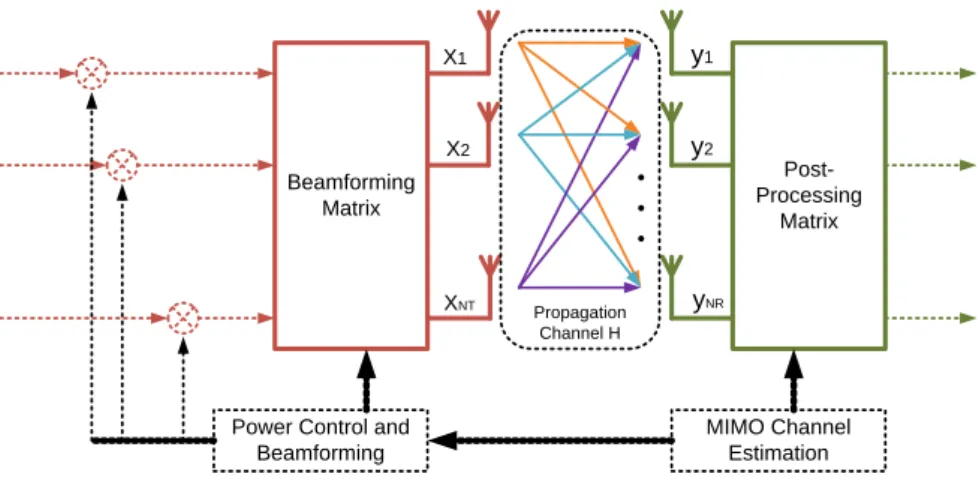
When both the transmitter and receiver are equipped with multiple antennas as shown in Fig.1.6, the pre-coding at the transmitter and post-processing at the receiver can be used to exploit the additional degree of freedom.
Beamforming Matrix Post-Processing Matrix Propagation Channel H X1 X2 XNT y1 y2 yNR
Power Control and Beamforming
MIMO Channel Estimation
Figure 1.6: Basic block diagram of a MIMO baseband transceiver.
Considering a MIMO system with NT transmit antennas and NRreceive antennas as shown in Fig.1.6, the received NR× 1 symbol vector, y = [y1, y2, · · ·, yNR]T, can be expressed as
Introduction 13
where x = [x1, x2, · · ·, xNT]T denotes the NT × 1 symbol vector to be simultane-ously transmitted over the NT transmit antennas, H is a NT × NR-dimension com-plex channel matrix with each element Hnr,nt, nr ∈ [1, NR]and nt ∈ [1, NT], w rep-resents the NR× 1 channel complex Gaussian noise with zero-mean and covariance
E[|w|2] = δw2INR. Therefore, each of the receive antennas obtains a signal which is a linear combination of all the transmitted signals, which could be expressed by
ynr = x1Hnr,1+ x2Hnr,2+ · · · + xNTHnr,NT + wnr (1.11)
With full CSI available at both the transmitter and receiver, the knowledge of H could be exploited to design the beamforming scheme at the transmitter and the post-processing scheme at the receiver. If the rank of H is M (M ≤ min{NT, NR}), it is possible to simultaneously transmit M individual symbols [25]. Let us decompose the MIMO channel matrix H by Singular-Value-Decomposition (SVD) as
H = UΣVH (1.12)
where U and V are the NR× NRand NT × NT unitary matrices respectively, Σ is a
NR× NT diagonal matrix which consists of singular values of H in a decreasing order. There are M nonzero singular values, represented by λ1≥ λ2 ≥ · · · ≥ λM, in Σ as the rank of the H is M . In the MIMO-SVD transmission [71], V is used for precoding or beamforming at the transmitter and U is employed for post-processing at the receiver. If we use {s1, s2, · · ·, sM}T to denote the symbols to be transmitted and assume that the knowledge of H is available at the transmitter, the symbols can be precoded as
x = Vs (1.13)
where s = [s1, s2, · · ·, sM, 0, · · ·, 0]T is a NT-size symbol vector.
At the receiver, the SVD of H could be exploited to carry out the post-processing and further to separate the transmitted symbols s. This can be achieved by employing
Uas the post-processing matrix as
z = UHy
= UHHx + w
= UH(UΣVH)Vs + w
= Σs + w (1.14)
14 Context and Motivation
matrix Σ in Eq. (1.14) is a diagonal matrix, so the MIMO-SVD system could be equiv-alently regarded as M parallel single-input-single-output (SISO) systems as shown in Fig.1.7. 1
2
M
1s
2s
Ms
1z
2z
Mz
1w
2w
M
Ms
Mz
Mn
Mw
Figure 1.7: Equivalent parallel SISO channel of MIMO-SVD. Therefore, the output of the mtheigenvalue channel could be expressed as
zm= λmsm+ wm, m = 1, 2, · · ·, M. (1.15) Based on the MIMO structure, let us take a linear precoding [107] as an example. In [107], the pre-coder consists of three separating processing blocks, i.e. orthogonal beam direction UP, per-beam power allocation DP and input shaper VP. The SVD of the precoder matrix could be expressed as
P = UPDPVP (1.16)
To conserve the total transmit power, the precoder must satisfy
tr(PP∗) = 1 (1.17) That means the sum of the power over all beams is limited. However, the individual beam power can be allocated dynamically according to the beam quality or the design criterion.
In the MIMO-SVD system, the beam direction matrix UP could be chosen as V of the wireless MIMO channel H and the per-beam power allocation matrix DP can be determined according to the Water-Filling algorithm [34]. Then, the pre-coding structure could be illustrated as in Fig.1.8.
Introduction 15 Multimode Beamformer Matrix UP X1 X2 XNT Input Shaper Matrix VP d1 d2 dM u1 u2 uM d1 d2 dM
Figure 1.8: Structure of a linear pre-coder.
Generally, a pre-coder has two functions: (i) decoupling the input symbols into or-thogonal spatial modes and direct different symbols to different directions; (ii) allocat-ing power over these beams based on the channel state information at the transmitter (CSIT).
Multicarrier and Multiple Antenna System
MIMO-OFDMis a cooperative combination of the MIMO and OFDM, which can en-hance the capacity and diversity and also can mitigate the detrimental effect due to the multipath fading. These benefits come from the advantages of the MIMO and OFDM individually.
OFDM is a block modulation scheme where a block of N symbols is modulated in parallel on N subcarriers as shown in Fig.1.4, which can be implemented by using an IDFT. The time interval of an OFDM symbol is N times that of the single-carrier sys-tem when the syssys-tem has the same bandwidth. In order to mitigate the inter symbol interference (ISI) induced by the time spread of the wireless multi-path channel, each
16 Context and Motivation
block of N symbols at the output of the IDFT is typically preceded by a CP or guard interval consisting of Nguardsamples which is at least equal to the channel length.
Un-der this condition, a linear convolution of the transmitted sequence and the channel becomes a circular convolution. Then, the ISI can be easily and completely eliminated. Moreover, the equalization of an OFDM receiver can be carried out by one tap equal-izer in the frequency domain.
A MIMO system could take advantage of spatial diversity which is obtained by spatially separated antennas in a multi-path scattering environment [100] to enhance the system performance.
In most of radio environments, the wireless channel is a multi-path scattering channel which could degrade the reception performance of the conventional wireless techniques. Fortunately, OFDM can overcome the effect of various multi-path channel and MIMO could take advantage of multi-path scattering. Therefore, combining the techniques of the OFDM and MIMO to construct MIMO-OFDM system is a promis-ing technique to provide high data rate wireless transmission in the harsh wireless environment.
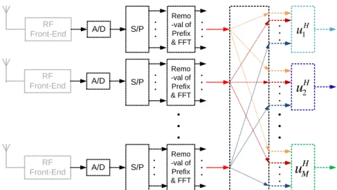
We consider a MIMO-OFDM system based on the MIMO system with NT transmit
antennas and NRand the OFDM system with N size IDFT/DFT as presented in the previous Subsection. The MIMO-OFDM baseband transmitter is illustrated as in Fig.
1.9and the corresponding baseband receiver is as shown in Fig.1.10.
IFFT and Prefix IFFT and Prefix IFFT and Prefix P/S P/S P/S D/A RF Front-End D/A RF Front-End D/A RF Front-End A/D RF Front-End A/D RF Front-End Remo -val of Prefix & FFT Remo -val of Prefix & FFT S/P S/P H
u
1 Hu
2 1 V 2 V M VFigure 1.9: Illustration of a MIMO-OFDM transmitter.
Although the MIMO-OFDM based physical layers have greatly improved the ca-pacity of radio link, the radio link caca-pacity still can not meet the explosive rise of the data rate demand. Therefore, more advanced physical techniques and more flexible
Introduction 17 IFFT and Prefix IFFT and Prefix IFFT and Prefix P/S P/S P/S D/A RF Front-End D/A RF Front-End D/A RF Front-End A/D RF Front-End A/D RF Front-End A/D RF Front-End Remo -val of Prefix & FFT Remo -val of Prefix & FFT Remo -val of Prefix & FFT S/P S/P S/P H
u
1 Hu
2 H Mu
1 V 2 V M VFigure 1.10: Illustration of a MIMO-OFDM receiver.
radio transceivers need to be developed to approach this goal. However, fully ex-ploiting these gains comes, in general, at the cost of significantly increasing in signal-processing complexity, especially in the receiver.
Therefore, exploring a flexible and agile radio transceiver is great rewarding to provide high physical layer capacity for the future wireless network.
1.2.2
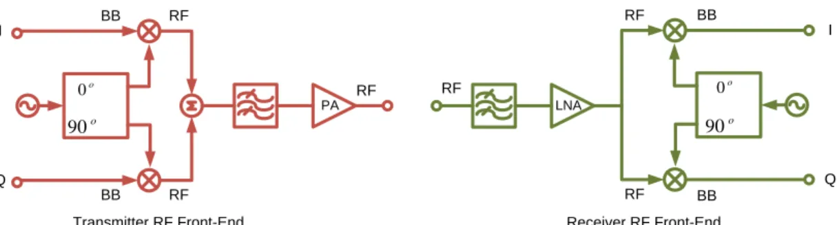
Transceiver RF Front-End
In the wireless system, the transmitter RF front-end is used to up-convert the analog baseband signal to the RF signal which is suitable for transmission over the wireless channel, while the receiver RF front-end is employed to down-convert the RF signal to the baseband signal. The receiver RF front-end always attracts more research atten-tions, because it is more closely related to signal reception and recovery. Generally, the traditional radio receivers are divided into Zero-IF receivers and Superheterodyne receivers which are correspondent to Zero-IF RF front-ends and superheterodyne RF front-ends respectively.
Zero-IF RF Front-End
In the Zero-IF or direct conversion RF front-end, the received RF signal is directly down-converted to the Zero-IF frequency [123] signal. A typical architecture of the Zero-IF RF front-end is as shown in Fig. 1.11. In this architecture, it is not necessary to require external high Q image rejection filter. Besides, a simple low pass filter (LPF) can be used to fulfill the channel selection.
18 Context and Motivation u2 d2 LNA LNA o 0 o 90 PA LNA o 0 o 90 RF RF RF RF RF RF BB BB BB BB I Q Q I
Transmitter RF Front-End Receiver RF Front-End
Figure 1.11: Simplified architecture of a direct conversion transmitter and re-ceiver RF front-end.
biggest weakness of this architecture is that the local oscillator (LO) leakage to the mixer could result in self-mixing, which causes a time-varying direct conversion (DC) offset at the output of the mixer. Also, the Zero-IF RF front-end is sensitive to the I/Q imbalance. The gain and phase mismatch could significantly degrade the image rejection.
Superheterodyne RF Front-End
Armstrong proposed the superheterodyne receiver architecture in 1918 [16]. Most of the current radio transceivers still use similar approach for the frequency updown conversion with some refinements. Fig. 1.12shows the block diagram of a super-heterodyne RF front-end. u2 d2 LNA LNA LNA o 0 o 90 RF RF RF BB BB Q Receiver RF Front-End IF VCO1,f1 VCO2,f2 RF Filter Rejection FilterImage Select FilterChannel
Figure 1.12: Simplified architecture of a superheterodyne RF front-end. As we can see, the received RF signal is filtered by a RF band pass filter (BPF) first, then amplified by a low noise amplifier (LNA), after that down-converted to a inter-mediate frequency (IF) signal by using a mixer with carrier frequency f1. After the
image rejection filter, this IF signal is down-converted by another mixer with carrier frequency f2, (f2 < f1). The channel selecting filter selects the desired signal and
out-put the desired baseband analog signal. The major advantages of this radio receiver based on the superheterodyne RF front-end are its high sensitivity, excellent selectivity and good image rejection. The major drawback of this radio receiver is that it requires high Q filters to fulfill the image rejection.
Introduction 19
1.3
Contribution and Outline
This dissertation is part of research effort to:
• put the concept of Full-Duplex into practice • develop an agile radio transceiver
for improving the spectral efficiency and providing high data rate for future wireless networks, like the 5G or cognitive radio networks.
1.3.1
Contribution
The contributions of this dissertation to the research effort are threefolds:
I. Self-Interference Cancellation: With respect to the Full-Duplex OFDM wire-less, the interference (SI) after the implementation of the active analog RF self-interference cancellation (AARFSIC) is still very strong. We dig deeply the characters of the residual SI and then propose an active digital self-interference cancellation in time domain (ADSICT) to eliminate it. The proposed ADSICT can bring down the residual SI to the noise floor.
II. Full-Duplex Wireless Radio: We design an in-band Full-Duplex OFDM radio node equipped with two antennas. The performance of the designed radio is eval-uated by system level simulation and the impacts of the RF impairments (receiver thermal noise, phase noise in the local oscillator) on the Full-Duplex OFDM radio are qualified and then reduced or avoided.
III. Full-Duplex Dual-Band Wireless Radio:The flexible radio front-end based on the Full-Duplex radio and Dual-Band RF front-end is theoretically demonstrated and designed. The Full-Duplex Dual-Band OFDM (FDDB) radio transceiver based on the proposed RF front-end can simultaneously process two separate spectrum fragment signals. However, the I/Q imbalance significantly degrades the performance of the proposed radio transceiver. Therefore, we developed a suitable and advanced I/Q imbalance compensation method which could significantly eliminate the impact of the I/Q imbalance.
1.3.2
Thesis Outline
20 Contribution and Outline
Part I:
In this part, we present the Self-Interference Cancellation (SIC) schemes in details for the Full-Duplex wireless radio including the Chapter 2 and Chapter 3.
Chapter 2. gives the reviews about the state-of-the-art of the SIC schemes includ-ing antenna cancellation, passive interference suppression (PSIS) and active self-interference cancellation (ASIC). Besides, the key factors limiting the performance of the SIC are analyzed and studied.
Chapter 3. digs deeply the AARFSIC in the Full-Duplex OFDM wireless with one-path SI channel and multi-one-path SI channel, as well as finds the core problem limiting the capability of the SIC in the multi-path scenario. Then, the developed SIC which is based on the AARFSIC and ADSICT for the Full-Duplex OFDM wireless is presented.
Part II:
In this part, we present the design of a Full-Duplex OFDM wireless radio in details.
Chapter 4.gives the design and evaluation of an in-band two-antenna Full-Duplex OFDM wireless radio with one-path SI channel and multi-path SI channel. The impact of the Phase Noise on the Full-Duplex OFDM radio is qualified. Besides, the effect of the receiver Thermal Noise on the ASIC is elaborated and reduced.
Part III:
In this part, we present the design of a Full-Duplex Dual-Band (FDDB) wireless radio including Chapter 5.
Chapter 5. presents a FDDB radio based on the Full-Duplex radio and Dual-Band RF front-end at first. Then, the design of a FDDB OFDM radio transceiver is given. After that, a simple but practical I/Q imbalance estimation and compensation method based on the frequency-flat-fading behaviors of the SI channel is proposed. Finally, the proposed FDDB OFDM radio and the developed I/Q imbalance mitigation algorithm are evaluated by system level simulation.
Part IV:
In this part, we present the conclusions and future outlook of this dissertation.
Introduction 21
1.4
Related Publications
Related Publications
Chapter 3 revises the related publications [116,117]. Chapter 4 revises the related publications [116,117,118]. Chapter 5 revises the related publications [119,120,121].
Part I
Self-Interference Cancellation in
Full-Duplex Wireless
2
State-of-the-Art of the
Self-Interference Cancellation
Full-Duplex is a promising technique for supporting simultaneous transmission and reception at the same radio frequency band. Therefore, Full-Duplex wireless radio has emerged as an attractive solution to improve the efficiency of the spectrum utilization and to enhance the flexibility of radio transceivers. However, a key challenge behind the Full-Duplex is how to manage or cancel the so called self-interference (SI) induced by the leakage of its own transmission to the desired reception to a tolerable level.
In order to overcome the strong SI faced by the Full-Duplex wireless radio system, lots of efforts have been devoted to handle the strong SI. The researchers at the Univer-sity of Waterloo [60,61], Stanford University [30], NEC Lab and Princeton University [17, 83] propose interference nulling or canceling from the perspective of antennas. The researchers at Rice University [41] study the passive self-interference suppression (PSIS) including directional isolation, absorptive shielding and cross polarization. Be-sides, [19,30,39,55,56,72,95] focus on the active self-interference cancellation (ASIC). In this Chapter, these three schemes (antenna cancellation, PSIS and ASIC) are pre-sented in details. Furthermore, the factors limiting the performance of the ASIC are introduced.
26 Antenna Cancellation Rx RF Front-End Tx RF Front-End d d
/2 Power Splitter Tx1 Rx Tx2Figure 2.1: The block diagram of the SAC.
2.1
Antenna Cancellation
Antenna cancellation is a SIC method that employs multiple antennas to make the RF signals add destructively at the receiver antenna, or to obtain an inverse version of the received RF signal by internal phase shifting by 180oand then subtract it at the RF part. There are mainly two antenna cancellation schemes, which will be presented in details in the following.
2.1.1
Antenna Cancellation based on λ/2 Spacing
In the Stanford Antenna Cancellation (SAC) [30], the Full-Duplex radio node employs three antennas, among which two antennas are used for transmission and the other one is used for reception. Besides, the radio node is equipped with two RF front-ends. One is used for up-converting the baseband transmit signal to the radio frequency (RF) signal. The other one is used for down-converting the received RF signal to the baseband analog signal. In order to make the two received RF signals from its own two transmit antennas add destructively, the receive antenna is placed such that the distance from the two transmit antennas to the receive antenna differs by half of the wavelength of the center carrier frequency. Fig. 2.1shows the block diagram of the SAC. Let x(t) be the unit power baseband transmit signal, Pt1 and Pt2be the transmit power of the two signals from the two transmit antennas respectively, L1 and L2
de-note the attenuations experienced by the two transmit signals before arriving at the receive antenna, d1 and d2 represent the distance from the two transmit antennas to
the receive antenna respectively. The residual SI signal after the interference nulling, i.e. SAC, rSACres(t), is given by
rSACres(t) = p Pt1 p L1x(t)e2πfc(t+ d1 c)+pPt2pL2x(t)e2πfc(t+d2c) (2.1)
State-of-the-Art of the Self-Interference Cancellation 27 Rx RF Front-End Tx RF Front-End d d Power Splitter Tx1 Rx Tx2
Figure 2.2: Block diagram of the Transmit Antenna Cancellation.
where fc denotes the center carrier frequency and c is the speed of light. If d2 =
d1+ λ2, where λ is the wavelength of the carrier frequency fc, these two signals add
destructively and hence the SI signals can be nulled.
The experimental results in [30] show that this antenna cancellation could achieve 30dB of interference cancellation. However, this scheme could only be used for narrow-band signals because of its high dependency on the wavelength.
2.1.2
Antenna Cancellation based on Symmetry
Waterloo Antenna Cancellation based on Symmetry
The Waterloo Antenna Cancellation (WAC) [60] is based on the symmetric placement of the antennas. The block diagram of the WAC is as shown in Fig. 2.2. The two transmit antennas are placed symmetrically relative to the receive antenna. The signal from the transmit antenna-1 (Tx1) is phase shifted internally by a fixed π phase shifter. Then, the received residual SI signal, rWACres, after the WAC is represented by
rWACres(t) = p Pt1 p L1x(t)e[2πfc(t+ d c)+π]+pPt2pL2x(t)e2πfc(t+ d c) (2.2)
The two copies of the signal add π out of phase could null each other. This scheme uses the fixed π phase shifter instead of offsetting the distance by λ2 to obtain the inverse version of the other signal. The experimental results in [17,83] show that the WACcould achieve 22 to 30dB of SIC.
NEC-Princeton Antenna Cancellation based on Symmetry
The NEC-Princeton Antenna Cancellation (NEC-PAC) is also based on the symmetric placement of the antennas. Based on the architecture, the PAC includes NEC-Princeton Transmit Antenna Cancellation (NEC-PTAC) and NEC-NEC-Princeton Receive
28 Antenna Cancellation Tx RF Front-End Rx RF Front-End d d Power Combiner Rx1 Tx Rx2
Figure 2.3: Block diagram of the Receive Antenna Cancellation. Antenna Cancellation (NEC-PRAC).
NEC-PTAC:The block diagram of the NEC-PTAC scheme is similar to WAC, there-fore be dropped here. The expression of the received residual SI, rNEC-PTAC, after the
NEC-PTACis similar to Eq. (2.2).
NEC-PRAC:The block diagram of the NEC-PRAC scheme is as shown in Fig. 2.3. The two receive antennas are placed symmetrically relative to the transmit antenna. The signal received by the Rx1 is phase shifted internally by a fixed π phase shifter. After combining the two received signals by Rx1 and Rx2 at the power combiner, the residual SI, rNEC-PRACres(t), is expressed as
rNEC-PRACres(t) = p Pt p L1x(t)e[2πfc(t+ d c)+π]+pPtpL2x(t)e2πfc(t+ d c) (2.3)
where Ptdenotes the transmit power of the baseband signal x(t). If L1 = L2, these
two received RF signals could cancel each other by adding destructively.
NEC-PAC: The NEC-PAC is a cancellation method based on the NEC-PTAC and
NEC-PRAC. The block diagram of the NEC-PAC is as shown in Fig.2.4. Two Rx anten-nas are placed symmetrically on the perpendicular bisector of the two Tx antenanten-nas. The transmit signal from the Tx1 is phase shifted by π before emission. Each Rx will first receive the SI after the NEC-PTAC. Furthermore, the received residual SI by Rx1 is phase shifted by π via using a fixed π phase shifter before being combined with the other received residual SI signal. Therefore, the NEC-PAC includes two levels of SIC.
The residual SI received by the Rx1 after the NEC-PTAC is
rRx1,NEC-PTACres(t) = p Pt1 p L11x(t)e[2πfc(t+ d11 c )+π]+pPt2pL12x(t)e2πfc(t+d12c ) (2.4) where L11and L12denotes the path fading loss from Tx1 and Tx2 to Rx1 respectively,
d11represents the distance between Tx1 and Rx1 and d12represents the distance
State-of-the-Art of the Self-Interference Cancellation 29 Rx RF Front-End Tx RF Front-End Splitter Tx1 Tx2 Rx1 Rx2 Combiner
Figure 2.4: Block diagram of the NEC-PAC.
The residual SI received by the Rx2 after the NEC-PTAC is
rRx2,NEC-PTACres(t) = p Pt1 p L21x(t)e[2πfc(t+ d21 c )+π]+pPt2pL22x(t)e2πfc(t+d22c ) (2.5) where L21and L22denotes the path fading loss from Tx1 and Tx2 to Rx2 respectively,
d21represents the distance between Tx1 and Rx2 and d22represents the distance
be-tween Tx2 and Rx2.
The residual SI, rNEC-PACres(t), after the two levels of SIC (PTAC and NEC-PRAC) can be given by
rNEC-PACres(t) = rRx1,NEC-PTACres(t)e
π+ r
Rx2,NEC-PTACres(t) (2.6)
[17] experimentally demonstrates that the PAC could provide up to 45dB of SIC in a wireless environment with few multiple reflecting paths.
In fact, the schemes of the WAC, SAC and NEC-PAC are based on the principle of interference nulling which has high requirement on symmetries: power symmetry, placement symmetry of antennas, fading loss symmetry and channel symmetry. The first two symmetries can be guaranteed, because power allocation and placement of the antennas can be implemented exactly. However, the channel symmetry is depen-dent on the wireless environment. If in an anechoic chamber, which means the SI channel is a line-of-sight (LoS) path channel, the demand of channel symmetry can be met. While if in a chamber with rich reflections, the channel symmetry may not hold for the strong non-line-of-sight (NLoS) components. That is why antenna cancellation could achieve more SIC in the wireless environment with few reflectors as stated in [17,83].
30 Passive Self-Interference Suppression
Another antenna cancellation technique proposed in [104] has been experimen-tally demonstrated by [42]. The experimental results show that this antenna cancella-tion based on the combinacancella-tion of null-steering beamforming and antenna polarizacancella-tion diversity could achieve up to 66dB of SIC but still in an anechoic chamber.
2.2
Passive Self-Interference Suppression
The basic principle of the PSIS is to use the electromagnetic isolation techniques to reduce the power of the leaked signal from its own transmission to the receiver. The PSIS includes antenna separation, directional antenna, absorptive shielding and an-tenna polarization. Anan-tenna separation is one of the simplest ways of PSIS, which could result in around 40dB of the SI suppression when the antennas are separated by 30 centimeters. Directional antenna could result in 36 ∼ 38dB of SI suppression depending on the configuration [41]. Absorptive shielding can provide up to 25dB ab-sorption [41]. Antenna polarization in the near-field wireless communications could achieve 10dB of SI isolation [17].
2.3
Active Self-Interference Cancellation
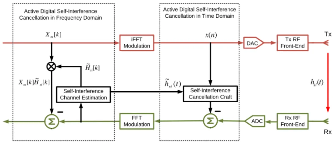
ASICis a method to exploit the knowledge of its own transmission and emulate the over-the-air SI channel to craft a cancellation signal and then subtract it in the receiver chain. The classical radio receiver and potential placement of the SIC is as shown in Fig. 2.5. Based on the SIC being implemented before or after the Analog-to-Digital Converter (ADC), the ASIC is classified as Active Analog Self-Interference Cancella-tion (AASIC) and Active Digital Self-Interference CancellaCancella-tion (ADSIC).
C
f
ADC DemappingDigital
LPF VGA
VG-LNA
AGC
+
Analog RF Cancelation Signal
+
Digital Cancelation Signal
+
Analog BB Cancelation Signal