HAL Id: hal-01633146
https://hal.archives-ouvertes.fr/hal-01633146
Submitted on 29 Jan 2018
HAL is a multi-disciplinary open access
archive for the deposit and dissemination of
sci-entific research documents, whether they are
pub-lished or not. The documents may come from
teaching and research institutions in France or
abroad, or from public or private research centers.
L’archive ouverte pluridisciplinaire HAL, est
destinée au dépôt et à la diffusion de documents
scientifiques de niveau recherche, publiés ou non,
émanant des établissements d’enseignement et de
recherche français ou étrangers, des laboratoires
publics ou privés.
Origin and repartition of the oxide fixed charges
generated by electrical stress in memory tunnel oxide
S. Bernardini, P. Masson, M. Houssa, F. Lalande
To cite this version:
S. Bernardini, P. Masson, M. Houssa, F. Lalande. Origin and repartition of the oxide fixed charges
generated by electrical stress in memory tunnel oxide. Applied Physics Letters, American Institute of
Physics, 2004, 84 (21), pp.4251-4253. �10.1063/1.1756681�. �hal-01633146�
Origin and repartition of the oxide fixed charges generated by electrical stress in
memory tunnel oxide
Sandrine Bernardini, Pascal Masson, Michel Houssa, and Frederic Lalande
Citation: Applied Physics Letters 84, 4251 (2004); doi: 10.1063/1.1756681
View online: http://dx.doi.org/10.1063/1.1756681
View Table of Contents: http://scitation.aip.org/content/aip/journal/apl/84/21?ver=pdfcov Published by the AIP Publishing
Articles you may be interested in
Charge storage properties of InP quantum dots in GaAs metal-oxide-semiconductor based nonvolatile flash memory devices
Appl. Phys. Lett. 101, 212108 (2012); 10.1063/1.4767522
Study of the relative performance of silicon and germanium nanoparticles embedded gate oxide in metal–oxide–semiconductor memory devices
J. Appl. Phys. 109, 064504 (2011); 10.1063/1.3555087
Bandgap engineering of tunnel oxide with multistacked layers of Al 2 O 3 / HfO 2 / SiO 2 for Au-nanocrystal memory application
Appl. Phys. Lett. 93, 132907 (2008); 10.1063/1.2995862
Comparison of structural and electrical properties of praseodymium oxide and praseodymium titanium oxide charge trapping layer memories
J. Appl. Phys. 102, 074111 (2007); 10.1063/1.2786102
Conduction mechanisms and charge storage in Si-nanocrystals metal-oxide-semiconductor memory devices studied with conducting atomic force microscopy
J. Appl. Phys. 98, 056101 (2005); 10.1063/1.2010626
This article is copyrighted as indicated in the article. Reuse of AIP content is subject to the terms at: http://scitation.aip.org/termsconditions. Downloaded to IP: 155.97.178.73 On: Tue, 24 Jun 2014 10:30:29
Origin and repartition of the oxide fixed charges generated by electrical
stress in memory tunnel oxide
Sandrine Bernardini, Pascal Masson,a)Michel Houssa,b) and Frederic Lalande
L2MP, UMR-CNRS 6137, IMT Technopoˆle de Chateau Gombert, 13451 Marseille Cedex 20, France
共Received 10 November 2003; accepted 1 April 2004; published online 7 May 2004兲
A method is proposed to determine the origin and the spatial oxide fixed charge repartition in memory tunnel oxide from Fowler–Nordheim current measurements after electrical stress. The Poisson equation resolution in the dielectric layer is required to account for the nonsymmetric tunneling barrier deformation, resulting from charges generated within the dielectric layer. From current–voltage characteristics measurements and simulations, we have determined the spatial distribution of the oxide fixed charges within the dielectric layer of metal/SiO2/metal structures. In addition, the kinetics of the oxide charge generation can be explained by a dispersive hydrogen transport model. © 2004 American Institute of Physics. 关DOI: 10.1063/1.1756681兴
Usually, the tunneling current flowing through the gate insulator in metal–oxide–semiconductor共MOS兲 structures is calculated without considering the influence of dielectric bulk charges on the shape of the tunneling barrier.1–3 How-ever, it is well known that the electrical properties of MOS structures depend much on electrically active defects. In this work, we describe a method to determine the nonuniform dielectric fixed charge distribution induced by electrical stress of metal/SiO2/metal structures, based on the analysis
of tunneling currents after electrical stress. Our approach lies in the continuity of the work of Ku et al.4 which have per-formed an analytical resolution of Poisson equation in the case of a uniform fixed charge repartition. It is also shown that the kinetics for the oxide fixed charge buildup can be explained by a dispersive hydrogen transport model.
In this study, the tunneling oxide capacitor, with area
W⫻L⫽1000⫻75m2, is assumed to be equivalent to three series capacitances:5 a highly doped silicon electrode 共n type兲 with NSub⫽1.5⫻1025m⫺3, an oxide layer with t
ox
⫽8.3 nm, and a highly doped n-type polysilicon electrode 共gate electrode兲 with NG⫽1.2⫻1026 m⫺3. The relationship
between the two surface potentials,⌿Sand⌿G共for the sub-strate and the gate, respectively兲, and the gate voltage, VGB, is given by VGB⫽⌽MS⫺ Qox eff Cox ⫹⌿S⫺⌿G⫺ QSC共⌿S兲 Cox , 共1兲
where Cox is the oxide capacitance, ⌽MS is the gate–
semiconductor work function difference, QSC is the total
bulk charge, and Qox effis the effective charge density seen
from the bulk interface. For a given gate voltage and a given dielectric charge density, the spatial distribution of the di-electric potential, V, is calculated from Poisson resolution within the dielectric layer using a three-point finite difference method and the following boundary limits:
再
V共y⫽0兲⫽0 V共y⫽t ox兲⫽⫺ QSC⫹Qox eff Cox , 共2兲where y is the distance from the bulk 共silicon electrode兲. Then, using Wentzel–Kramer–Brillouin approximation,6 we express the current, due to the tunneling of electrons from the substrate to the gate (Isi) and from the gate to the
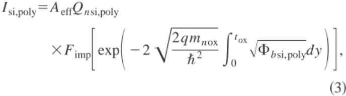
sub-strate (Ipoly), respectively, Isi,poly⫽AeffQnsi,poly
⫻Fimp
冋
exp冉
⫺2冑
2qmnox ប2冕
0 tox冑
⌽bsi,polydy冊册
, 共3兲where Aeff is the effective area of the capacitor, Qn is the inversion charge in the substrate (Qnsi) and in the gate (Qnpoly), Fimp is the impact frequency, ⌽b, is the barrier height between the silicon,⌽bsi共or polysilicon, ⌽bpoly) con-duction band and the dielectric concon-duction band, and mnoxis
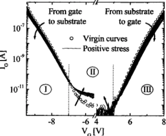
the electron mass in oxide. Figures 1 and 2 illustrate the current–voltage (I – V) characteristics of two different ca-pacitors measured after cumulative times of negative 共⫺9.5 V兲 and positive 共8 V兲 gate voltage stress, respectively.
a兲Author to whom correspondence should be addressed; electronic mail:
b兲Present address: IMEC, 75 Kapeldreef, B-3001 Leuven, Belgium. FIG. 1. I – V characteristics of the capacitor recorded after cumulative timesof negative gate voltage stress共⫺9.5 V兲.
APPLIED PHYSICS LETTERS VOLUME 84, NUMBER 21 24 MAY 2004
4251
0003-6951/2004/84(21)/4251/3/$22.00 © 2004 American Institute of Physics
This article is copyrighted as indicated in the article. Reuse of AIP content is subject to the terms at: http://scitation.aip.org/termsconditions. Downloaded to IP: 155.97.178.73 On: Tue, 24 Jun 2014 10:30:29
In Figs. 1 and 2, we will only discuss parts I and III which correspond to a decrease in the Fowler–Nordheim tunneling current. This phenomenon is well known as the closure of the programmable window observed after numer-ous write–erase operations inEEPROMcells.7We observe, in Figs. 1 and 2, a more pronounced current decrease for the injection of electrons from gate to substrate for a negative stress, and from the substrate to the gate for a positive stress. Based on this dissymmetric behavior of the tunneling cur-rent, we have compared three different negative oxide fixed charge distributions: Constant, Gaussian, and exponential. The constant oxide fixed charge distribution did not allow us to fit the experimental data for both positive and negative voltages. This result shows that the distribution of the fixed charge, generated by electrical stress within the dielectric layer, is nonuniform. In the following, we detail only our results for positive stress.
Considering a Gaussian oxide charge repartition, the maximum of charge density must be located close to the substrate/oxide interface. However, the best fits to the data
共shown as solid lines in Fig. 3兲 have been obtained by
con-sidering a decreasing exponential charge distribution共cf. Fig. 4兲:
Qox⫽Qmaxexp
冉
⫺y
冊
⫹Qmin, 共4兲where Qminis the oxide charge in the virgin sample, Qmaxis
the maximum value of the oxide trapped charges during the stress, and is the decay length. The increases in the 兩Qmax兩
and values 共from 0 to 450⫻104 C m⫺3and from 0 to 16.25 Å, respectively兲 correspond to a trapped oxide charge mov-ing away from the interface durmov-ing the electrical stress. Let us remark that the determination of the oxide charge distri-bution using the two-level charge pumping technique on MOS transistors after electrical stress shows the same kind of spatial distribution for the oxide traps.8
Figure 5 shows the impact of a negative fixed charge in the dielectric layer close to the silicon electrode, which in-duces a band diagram deformation on this area. This result can only be obtained by Poisson resolution within the dielec-tric layer. It clearly appears that after positive stress, electron tunneling current is more degraded for a positive voltage than for a negative voltage 共cf. Fig. 2兲. Symmetrically, in case of negative stress共cf. Fig. 1兲, the induced fixed charges would be located close to the polysilicon electrode. Let us remark, that for EEPROM cells, the write–erase operations would lead to two decreasing exponential distributions of the oxide fixed charges共one on the silicon side and the other on the polysilicon side兲 which form one U-shaped curve.
A possible origin for the exponential negative fixed charge distribution in the oxide can be the release of hydro-gen species at the Si/SiO2interface by an impacting electron
during the stress. Then, the hydrogen species transport throughout the gate oxide and their subsequent trapping into
FIG. 2. I – V characteristics of the capacitor recorded after cumulative times of positive gate voltage stress共8 V兲.
FIG. 3. Comparison of simulated and measured I – V characteristics of the capacitor after cumulative positive stress, under gate injection and substrate injection.
FIG. 4. Decreasing exponential distribution of the trapped oxide charges used to fit the measurements shown in Fig. 3.
FIG. 5. Band diagram obtained with and without Poisson resolution within the SiO2layer for the exponential negative fixed charge distribution at VG
⫽8 V after 165 min.
4252 Appl. Phys. Lett., Vol. 84, No. 21, 24 May 2004 Bernardiniet al.
This article is copyrighted as indicated in the article. Reuse of AIP content is subject to the terms at: http://scitation.aip.org/termsconditions. Downloaded to IP: 155.97.178.73 On: Tue, 24 Jun 2014 10:30:29
the oxide network lead to the generation of SiuOuH de-fects close to the interface. These dede-fects are efficient elec-tron trapping centers,9 forming SiO⫺ defects which could correspond to the negative oxide charge generated during the stress. From these assumptions, the kinetics of SiuOuH precursor sites generation has been calculated within a dis-persive transport model,10,11 where the charge generation is assumed to be limited by the random hopping of H⫹and its trapping in the SiO2 layer.
Within this model,10the kinetics of charge density varia-tion ⌬Noxis given by
⌬Nox⫽NH⫹
冉
1⫺冕
01
SiO2GSiO2共y兲dy
冊
, 共5兲where NH⫹ is the density of protons close to the Si/SiO2
interface and G( y ) is a function related to the probability
P(x,t) for finding a proton at a distance x at time t; the
‘‘improved trial function’’ described by McLean and Ausman12 is used here for approximating G(y ). In Eq.共5兲,
ᐉSiO2⫽xc/ᐉht␣, where xc is the position of the
hydrogen-induced defect centroid, ᐉh is the average proton hopping
distance, and ␣is a parameter characterizing the dispersive-ness of the proton transport in the material. We fixed here
ᐉh⫽2.5 Å and ␣⫽0.3, consistently with values reported in
SiO2.10,11 The kinetics of oxide charge generation derived
from the data in Fig. 3 are compared to the model in Fig. 6. A very good agreement is obtained, with realistic values for
NH⫹⫽4⫻1013cm⫺2 and xc⫽3 nm, suggesting that the
de-fect precursors for the negative charge generation could be SiuOuH centers.
To summarize, we have presented a method to determine the spatial oxide fixed charge repartition in memory tunnel oxide. This method is based on the Poisson equation resolu-tion in the dielectric layer and presents the advantage to con-sider an arbitrary spatial distribution of oxide fixed charges. From I – V measurements after positive 共or negative兲 stress and Poisson resolution within the dielectric layer, we have found a decreasing exponential distribution of the fixed di-electric charge with a maximum value at the substrate/SiO2
共or SiO2/gate) interface. A possible explanation for this
de-creasing exponential distribution has been given from the generation of SiuOuH precursor defects close to the substrate/oxide interface, most probably leading to the cre-ation of SiO⫺ charges upon subsequent electron trapping.
1Y. Yang, H. Niimi, and G. Lucovsky, J. Appl. Phys. 83, 2327共1998兲. 2Y. Shi, X. Wang, and T. P. Ma, IEEE Electron Device Lett. 19, 388共1998兲. 3E. M. Vogel, K. Z. Ahmed, B. Hornung, W. K. Henson, P. K. McLarty, G. Lucovsky, J. R. Hauser, and J. J. Wortman, IEEE Trans. Electron Devices 45, 1350共1998兲.
4P. S. Ku and D. K. Schroder, IEEE Trans. Electron Devices 41, 1669
共1994兲.
5S. Bernardini, P. Masson, M. Houssa, and F. Lalande, ESSDERC共2003兲, p. 589.
6A. T. Fromhold, Quantum Mechanics for Applied Physics and Engineer-ing共Dover, New York, 1981兲.
7C. Papadas, G. Guibaudo, G. Pananakakis, C. Riva, and P. Ghezzi, IEEE Electron Device Lett. 13, 89共1992兲.
8
Y. Maneglia and D. Bauza, ICMTS’99共1999兲, p. 117.
9E. H. Nicollian and R. R. Brews, MOS Physics and Technology共Wiley, New York, 1982兲.
10M. Houssa, V. V. Afanas’ev, A. Stesmans, and M. M. Heyns, Semicond. Sci. Technol. 16, L93共2001兲.
11M. Houssa, A. Stesmans, R. J. Carter, and M. M. Heyns, Appl. Phys. Lett. 78, 3289共2001兲.
12F. B. McLean and G. A. Ausman, Phys. Rev. B 15, 1052共1977兲.
FIG. 6. Oxide charge kinetics comparison between the charge distribution used to fit the measurements shown in Fig. 3共open circles兲 and the simula-tions obtained from a dispersive transport model共solid line兲.
4253
Appl. Phys. Lett., Vol. 84, No. 21, 24 May 2004 Bernardiniet al.
This article is copyrighted as indicated in the article. Reuse of AIP content is subject to the terms at: http://scitation.aip.org/termsconditions. Downloaded to IP: 155.97.178.73 On: Tue, 24 Jun 2014 10:30:29