HAL Id: tel-00001905
https://tel.archives-ouvertes.fr/tel-00001905v2
Submitted on 1 Oct 2003HAL is a multi-disciplinary open access archive for the deposit and dissemination of sci-entific research documents, whether they are pub-lished or not. The documents may come from teaching and research institutions in France or abroad, or from public or private research centers.
L’archive ouverte pluridisciplinaire HAL, est destinée au dépôt et à la diffusion de documents scientifiques de niveau recherche, publiés ou non, émanant des établissements d’enseignement et de recherche français ou étrangers, des laboratoires publics ou privés.
To cite this version:
Henni Ouerdane. Influence of Ultrafast Carrier Dynamics on Semiconductor Absorption Spec-tra. Atomic Physics [physics.atom-ph]. Heriot Watt University, Edinburgh, 2002. English. �tel-00001905v2�
ON
SEMICONDUCTOR ABSORPTION SPECTRA
Henni Ouerdane
Submitted for the Degree of Doctor of Philosophy at Heriot-Watt University on completion of research in the
Department of Physics November 2001.
This copy of the thesis has been supplied on the condition that anyone who consults it is understood to recognise that the copyright rests with its author and that no quo-tation from the thesis and no information derived from it may be published without the prior written consent of the author or the university (as may be appropriate).
and has not been submitted for any other degree.
Henni Ouerdane
(Candidate)Dr. Ian Galbraith
(Supervisor)Date
tamet.t.ut ur nelli am tiyid..
Acknowledgements viii
Abstract xi
1 Introduction 1
1.1 Thesis layout . . . 8
2 Microscopic theory of polarization in semiconductor quantum-wells 11 2.1 Introduction . . . 11
2.2 Electrons in semiconductor quantum wells . . . 13
2.2.1 Physics of the 2D interacting electron gas . . . 13
2.2.2 Interacting electrons in a semiconductor quantum well . . . . 20
2.3 The Semiconductor Bloch Equations . . . 28
2.3.1 Hamiltonian equations . . . 28
2.3.2 Beyond the two-band approximation: the light hole contribution 37 2.4 Conclusion . . . 39
3 Numerical solutions of the semiconductor Bloch equations 41 3.1 Introduction . . . 41
3.2 Formulation of the numerical problem . . . 41
3.2.1 Simplifying the numerical work . . . 42
3.2.2 Evaluation of the Coulomb matrix elements . . . 43
3.3 The polarization function . . . 45
3.4 Absorption in a free carrier plasma . . . 48
3.4.1 Density dependence of the absorption spectra . . . 48
3.4.2 Temperature dependence of the absorption spectra . . . 49
3.5 Inclusion of the Coulomb interaction . . . 50
3.5.1 Many-body corrections . . . 50 iv
3.6 Beyond the simple calculations: more realistic absorption spectra . . 58
3.6.1 Effect of a finite well width . . . 58
3.6.2 Inclusion of the light hole . . . 59
3.6.3 Comparison between GaAs and ZnSe . . . 60
3.7 Refractive index spectra . . . 65
3.8 Discussion and conclusion . . . 66
4 Nonequilibrium carrier dynamics in semiconductor quantum-wells 68 4.1 Introduction . . . 68
4.2 Dynamical processes . . . 69
4.2.1 Time evolution of the carrier distributions . . . 69
4.2.2 Plasma cooling . . . 73
4.2.3 Time evolution of the plasma screening . . . 75
4.3 Initial conditions for the electron/hole plasma . . . 77
4.3.1 Selection rules for optical transitions . . . 77
4.3.2 The Gaussian hot carrier distribution . . . 78
4.4 Numerical results . . . 80
4.4.1 Time evolution of the carrier densities . . . 83
4.4.2 Time evolution of the plasma energy . . . 84
4.4.3 Time evolution of the plasma temperature . . . 86
4.4.4 Time evolution of the plasma screening . . . 87
4.5 Conclusions . . . 89
5 Ultrafast pump-probe dynamics in semiconductor quantum-wells 91 5.1 Introduction . . . 91
5.2 Ultrafast pump and probe experiments . . . 92
5.3 Numerical results . . . 95
5.3.1 Comparison between numerical and experimental results . . . 95 v
6 Exciton-electron scattering in semiconductor quantum-wells 106
6.1 Introduction . . . 106
6.2 Spontaneous emission rate in semiconductor quantum-wells . . . 108
6.2.1 The 2D electron/hole plasma . . . 108
6.2.2 Screened Coulomb potential . . . 109
6.2.3 The spontaneous emission rate . . . 110
6.3 Contribution of the free-carrier plasma to the spontaneous emission rate . . . 111
6.4 The exciton contribution to the spontaneous emission rate . . . 113
6.4.1 The ionization degree and modified law of mass action . . . . 114
6.4.2 The 2D exciton wave function . . . 119
6.4.3 The scattering matrix elements . . . 123
6.4.4 Fermi’s golden rule . . . 126
6.5 Numerical results . . . 129
6.5.1 The 2D exciton wavefunction . . . 129
6.5.2 The scattering matrix . . . 130
6.5.3 The free carrier contribution to the spontaneous emission rate 131 6.5.4 The exciton contribution to the spontaneous emission rate . . 132
6.5.5 The total spontaneous emission rate . . . 133
6.6 Discussion and conclusion . . . 134
7 Conclusion 137 A Plasma screening in the static plasmon-pole approximation 142 A.1 Derivation of the Lindhard formula . . . 142
A.2 The static plasmon-pole approximation . . . 145
A.2.1 The long wavelength limit . . . 145
A.2.2 The static plasmon-pole approximation . . . 146 vi
C Numerical evaluation of the Coulomb matrix elements 150 D Spontaneous emission and radiative lifetime in semiconductors 152 E Calculation of the exciton and free electron distributions 156
Publications 158
Bibliography 159
It is a great pleasure for me to be at this point of my work when I have the op-portunity to acknowledge and thank all the people who helped me, in one way or another, in preparing my PhD thesis during these three years in Edinburgh.
First of all, I wish to thank Dr Ian Galbraith for his excellent supervision during my time at Heriot-Watt University. I have greatly benefited from his thorough knowledge and expertise in semiconductor and computational physics. The countless discussions we have had and the explanations and original ideas he gave me were an invaluable contribution to this PhD thesis. In particular, I am most grateful for his assistance when I was writing the SBE codes. Being French made the work a little bit more challenging for both of us, but Ian always managed to put me at ease which helped overcome the barrier of languages. I have also appreciated his kind support and good advice for matters beyond my PhD work.
Dr Misha Portnoi and Dr Toni Lee’s help at the beginning of my PhD is also gratefully acknowledged. Toni’s expertise in UNIX and semiconductor physics was very useful in giving me a good start. Misha allowed me to use and modify some of his own computer codes to calculate the 2D excitonic wavefunctions in a screened Coulomb potential. Part of the work in chapter 6 was completed thanks to his help. I thank Mr George Papageorgiou for the guided tour of his lab and for giving me detailed information on the experimental setup as well as the experimental data used in chapter 5. I also thank Dr Chris Dent for proofreading the manuscript of this thesis and making useful suggestions.
Financial assistance through the Departmental Scholarship and additional fund-ing at the end of my PhD for which I thank Dr Ian Galbraith and Professor Brian Wherrett, are gratefully acknowledged.
I also want to thank my fellow PhD student and best friend, Brian Fleming. His solid friendship and support during these three years mean a lot to me. In particular, Brian’s ability to fix the numerous wee bugs I had to deal with still impresses me.
him, I could quickly cope with the computational part of my work. I wish these two geniuses great success with their own PhDs and all the best.
These past three years, I was extremely busy with my work, but I also managed to enjoy life in Scotland. Very many people contributed to the quality of my life here in Edinburgh. My mate Sean Kudesia taught me enough lingo to cope with everyday Scottish life, very useful to communicate with the lads in the pubs. Members of University staff (secretaries, cleaning ladies, shop assistants and refectory staff) were people with whom I had some of the most interesting and funniest chats. I had great time sharing a flat (and bills!) with my flatmates and friends Bruno Zettor and Sylvain N´eelz. I also had the privilege to share a bit of the life of two Scottish families and I want to thank them for all the good things they did for me. Lesley and Iain Maciver always considered me as a member of their family and I had great time in Balerno, appreciating Lesley’s delicious cuisine. The Saturday afternoons spent playing with James Ross are a source of great memories for me, and I thank Julie and Kenny Ross for their trust in letting me help them cope with James’ autistic condition as much as I could.
There is a lively contingent of foreign postgrads and RAs in the Physics Depart-ment, which create a very pleasant atmosphere. In particular, the Mediterranean connection composed of Spanish and Italian folks (David, Andrea, Manuela and Francesco) made me somewhat feel at home when we were speaking about the good things in life: food, olive oil and sun.
On a more personal basis, I would like to thank my fianc´ee Ioulia for her love, support and all the happiness she brings in my life. I also want to thank my family: my mother Ouiza, my sister Kahina, my brothers Djamel and Hac`ene, and my aunts Khalti Chabha and Khalti Ghenima for all the good they brought and are still bringing to my life.
Finally, and most importantly, this thesis is dedicated to my mother Ouiza, the ix
In this thesis, we present a theoretical description of the many-body effects in semi-conductor quantum wells and the role they play in the absorption phenomenon. The optical properties of semiconductors and their connections to the thermodynamic properties of the quasi-2D electron-hole plasma are studied in both nonequilibrium and equilibrium regimes. This work was motivated by a series of pump and probe experiments with spin-selective excitation that were performed at Heriot-Watt. The interpretation of the experimental results is non-trivial given the substantial influ-ence of Coulomb and many-body effects which give rise to a rich variety of broaden-ing and energy renormalizations, and hence places heavy demands on the modelbroaden-ing. We constructed a simple model to describe the nonequilibrium thermodynam-ics of the hot electron/hole plasma. We accounted for various dynamical processes such as: relaxation of the carrier distributions, thermalization, plasma cooling, car-rier spin-flip, recombination (radiative and nonradiative) and light hole scattering into heavy holes. A full microscopic treatment of the many-body problem being computationally prohibitive, we focused on a phenomenological approach using rate equations and the associated characteristic times for each of the dynamical process included in our analysis. We computed the time dependent energy renormalization and bleaching of the excitonic resonances by solving the semiconductor Bloch equa-tions together with the set of coupled rate equaequa-tions. We obtained a good qualitative agreement with experiments and further insight into the interplay between the var-ious dynamical processes by varying the phenomenological parameters entering the rate equations. In particular we found that the carrier spin-flip occurs on a relatively long time scale (several tens of picoseconds) compared to the carrier distributions relaxation and thermalization (a picosecond or less). We also could monitor the time evolution of the plasma density, energy, temperature and screening.
In this thesis, we also studied the photoluminescence in II−VI quantum wells at room temperature. We built a mathematical model to account for Coulomb
in these materials. We assumed the 1s exciton-free electron scattering to be the main process leading an exciton to the photon line before recombination. The excitonic wavefunctions in a 2D screened Coulomb potential were calculated using the variable phase method. The scattering matrix elements computed, we used Fermi’s golden rule to evaluate the contribution of the 1s exciton-free electron scattering to the spontaneous emission rate. PL spectra at room temperature were calculated for various densities, for wide-gap ZnSe and mid-gap GaAs to compare between II−VI and III−V materials. The ZnSe PL spectra exhibit an exciton resonance below the band edge that is not observed in the case of GaAs.
Introduction
In this thesis, we study the many-body effects in semiconductor quantum wells and the role they play in the absorption phenomenon. A semiconductor quantum well is an artificially grown structure in which the electron motion is confined in one spatial dimension, along the growth direction usually referred to as the z axis, and remains free in the xy plane. For example, it is possible to grow alternatively, on top of each other, layers of ZnSe with layers of CdxZn1−xSe. In quantum wells,
the kinetic energy of the charge carriers is quantized because of the confinement of their motion along the z axis; however, in the xy plane the motion of the carriers being not restricted, their kinetic energy may take continuous values. When excited, an electron leaves the valence band to go into the conduction band. This creates an empty valence-band state referred to as a hole that can be modeled as a quasi-particle with an effective mass, a spin and a momentum. To describe the excited electrons and holes trapped in a semiconductor quantum well, one usually makes use of the quasi-two-dimensional electron/hole plasma model [1]. This plasma may be neutral or not, depending on the excitation conditions achieved by optical pumping or carrier injection.
The electrons and holes interact through the infinite-range Coulomb interaction. A direct consequence is that their motion is correlated. Numerous experimental and theoretical studies have shown that Coulomb correlations between quasi-particles in-fluence the optical response of semiconductors [2, 3, 4]. For instance, excitons that are electron-hole bound states dominate the linear optical properties of semicon-ductors near the electronic bandgap. Another extremely important property of the carriers is related to their half-integer spin: electrons and holes are Fermions that obey the Pauli exclusion principle. The Fermionic nature of the carriers strongly
plasma (see chapters 2 and 3). In particular, when electrons are already occupying conduction band states, one cannot observe any optical transition leading a valence band electron to one of these occupied states. One refers to this as phase-space filling.
Modeling the properties of excited semiconductors can be tackled by studying separately the intraband interactions which influence the time evolution of the car-rier distributions, and the interband transitions to which the optical properties are mostly related. In order to describe and understand both types of phenomena a many-body treatment of the problem is required. The many-body effects are essen-tially due to the Coulomb interaction and carrier-phonon scattering. The transport properties connected with the intraband kinetics of electrons and/or holes are due to carrier-carrier interactions within the same band [5]. The consequences of such carrier-carrier interactions are the rapid equilibration (typically less than a picosec-ond [6]) of the electrons and holes into quasi-equilibrium Fermi-Dirac distributions, and the plasma screening which is the carrier density dependent weakening of the Coulomb interaction potential due to the presence of background charge carriers, i.e. the range of the Coulomb interaction decreases with increasing the carrier density. The spectral properties linked with the interband kinetics are due to the many-body interactions within the electron-hole plasma leading to the renormalization of the energy states. Thus, carrier-carrier scattering and carrier-phonon scattering1 are
the main contributers to the optical dephasing (the decay of the polarization of the medium) and influences both the shape (broadening) and the spectral location (energy shifts) of the absorption and refractive index spectra.
The study of the interplay between the Coulombic forces within the electron-hole plasma and the Fermionic nature of the charge carriers is a long standing problem that is still the object of intensive research (an excellent review paper [7] shows the importance of Coulomb correlations and other many-body interactions in the
physics of semiconductors). Theoretical and experimental work complement each other to provide information and further insight into the properties of semicon-ductors. Absorption experiments are often used to study the optical properties of semiconductors. In particular, ultrafast pump and probe experiments are a control-lable way of investigating the absorption properties of photoexcited semiconductors (see for instance [6, 8, 9, 10, 11, 12] and references therein). The main idea of the pump and probe beam technique is to excite the sample with an intense and spectrally narrow femtosecond laser beam and to probe changes in the absorption spectra with a weak2, spectrally broad probe beam. These changes are monitored
by comparing the spectra with the absorption spectrum obtained without the pres-ence of the pump pulse (linear absorption spectrum). Pump and probe pulse can be delayed with respect to each other to obtain femtosecond time resolution by mea-suring the absorption spectra as a function of the time delay. To understand these experiments a mean-field formalism has been developed: the semiconductor Bloch equations (SBE) [11, 13] are particularly appropriate to describe the density and temperature dependence of the light absorption in a semiconductor.
A semiconductor photoexcited by an ultrashort pulse passes through several regimes before it returns to thermodynamic equilibrium. The initial wavevector of the electron and of the hole is the same since the photon momentum is negligible. Thus an initial correlation exists between the electron and the hole. There is also a coherence between the carriers and the radiation field. This coherence is quickly broken by carrier-carrier scattering. The amount of time for the loss of coherence is called the dephasing time. If this time is faster than any other relaxation process, the carrier distribution functions are nonthermal even after the photo-excited states have lost their coherence. The appropriate formulation of the carrier dynamics for the time immediately after the generation of an electron-hole pair, when the photo-excited carrier states are still driven by their mutual coherence and their
2A crucial point for the pump and probe technique is the weak intensity of the probe beam: it
must be low enough to induce no changes of the optical properties, but it also has to be not too weak to give a reasonable signal-to-noise ratio.
body techniques [14, 15, 16].
Coherent effects can be studied using pump-probe spectroscopy with femtosec-onds pulses. Indeed, probing the response of a semiconductor with ultrashort laser pulses yields information on processes occuring faster than the fast equilibration time of the excited electron/hole system. In this case, the optical properties of direct-gap semiconductors exhibit some similarities to that of atomic systems. A coherent effect in semiconductors that has been extensively studied is the excitonic optical Stark effect (OSE). The OSE in atoms is a well-known phenomenon [11, 17, 18, 19], but its study in semiconductors has only been done with the possibility of performing ultra-fast optical experiments, as the dephasing time in semiconductors is much shorter than in atoms. The OSE process in semiconductors corresponds to a coupling of the energy levels with a below-gap light beam: there is a coherent modification of the energy levels in the electric field of the light field. The light is not absorbed, implying no real creation of quasi-particles in the semiconductor, therefore insur-ing an ultrafast response time [20]. The effect of the OSE is to shift the exciton absorption line during a laser pulse whose photon energy is below the absorption edge. The OSE in semiconductors has been the object of extensive experimental [21, 22, 23, 24] and theoretical [11, 14, 25, 26, 27, 28] investigations.
Of particular interest are also the effects of high-order correlations on the opti-cal properties of wide-gap semiconductors (WGSC), where Coulomb correlations are important because of the large exciton and biexciton binding energies, comparable to the room temperature thermal energy. For non-resonant (below exciton) excita-tion a red-shift of the exciton line arising from the influence of virtual transiexcita-tions to a bound biexcitonic state has been predicted [27, 29] and observed [30, 31]. For a gas initially comprised from a bath of free carriers, no spectral shift of the exciton line is seen [8]. As the carrier motions are increasingly correlated by the Coulomb interaction, creating bound excitons, the exciton resonance energy blueshifts due to exciton-exciton correlations [8]. For resonant excitation, the energy
renormal-izations due to the biexcitons are still unknown: one needs an accurate knowledge of the nature of the interacting electron-hole plasma to describe and explain both the magnitude and sign (blue- or red-shift) of these energy renormalizations. In materials such as ZnSe/ZnCdSe quantum-well, the high exciton binding energy (≈ 35 meV) allows resonant ultrafast optical excitation of excitons with negligible free carrier excitation. Recent experimental results obtained at Heriot-Watt [32] sug-gest that the interband recombination in WGSC (molecular-beam-epitaxially grown ZnSe/(Zn, Cd)Se/ZnSe multiple quantum well) at 4K is preceded by a phase dom-inated by biexcitons which induce a finite blue-shift of the exciton resonance. The experimental technique involved measuring the transmission of an extremely sta-ble white-light continuum probe-pulse which was delayed with respect to the 100 fs-long tunable pump pulse. Using circularly-polarized pump pulses resonant with the heavy hole exciton, a spin-polarized exciton population was generated. Mea-suring the transmission spectrum of an oppositely polarized probe, the biexciton absorption feature was directly detected.
Interpreting the experimental spectra is very difficult since it is non-trivial to estimate both the relative importance of the different contributions once they are clearly identified and the time-scale of the processes. Based on the interpretation one has then to build a model in which assumptions and approximations have at least to lead to results which reflect the qualitative behaviour of the physical quantities of in-terest. In fact, most of the theoretical treatments neglect the high-order correlations within the electron gas and they are still lagging the experimental results. Neverthe-less, as an improved level of the microscopic analysis of the Coulomb-induced many-body correlations is obviously required, efforts have been made to go beyond the time-dependent Hartree-Fock (TDHF) approximation. Indeed, some model studies [33, 34] in one dimension show clearly characteristic signatures of carrier-correlation effects on the excitonic differential absorption spectra. The analysis is done in both coherent [33] and incoherent [34] regimes.
the coherent limit [33, 35, 36]. But, due to dephasing processes occuring after some time when the excited system relaxes, the coherent limit is not valid. Then, both the pair occupations N and the exciton to two-exciton transitions, described by the six-particle correlation Z (involving three electron-hole pairs) [37, 38] have to be taken into account as they have finite values in this case. From an experimental point of view, N can be seen as the result of optical excitation at an earlier time, such that all coherences have decayed before the system is probed. Denoting p the optical interband polarization, one can obtain the coupled differential equation of motion for p and Z from the Heisenberg equation. But, the complete numerical solutions of these equations are currently not feasible in two dimensions and even for the one-dimensional systems one has to restrict oneself to small lattices and simplified Coulomb potential (tight-binding model with no screening).
To obtain further insight into the properties of the electron/hole plasma, it is possible to perform a series of pump-probe experiments introducing a variable delay between the two pulses. In particular, ultrafast nonlinear optical experiments allow one to probe highly nonequilibrium regimes and the possibility of non-degenerate pump and probe and spin-selective excitations makes the technique very powerful: one not only investigates the temperature and density dependence of the absorption spectra in the quasi-equilibrium regime but also tackles the challenging problem of the time evolution of the hot electron-hole plasma taking into account the spin-states of the carriers. Treating the full many-body problem is not feasible as it is computationally prohibitive: as we shall see in the next chapters, the equations involved become extremely complicated very quickly when one builds a rigorous model from first principles, and the singular behaviour of terms such as the Coulomb matrix elements makes the numerical work very challenging (see Chapter 3 and Appendix C).
In this thesis, we are concerned with ultrafast optical experiments. Interesting dynamical effects can arise as a result of coherent processes in the interaction of
the probe pulse with the relaxing electron/hole plasma, producing additional sig-nals that are not a direct result of carrier occupation functions. This complicates significantly the interpretation of experimental results. To avoid this type of compli-cation, we neglect coherent polarization nonlinearities, considering above bandgap pumping and time scales longer than the dephasing time only. Similar work has already been done for GaAs quantum wells at room temperature [39], but here, we account for various dynamical processes which lead the electron/hole plasma to quasi-equilibrium, at low temperature, and we also investigate the light hole exciton dynamics. For an in-depth discussion of the nonequilibrium problem see Ref. [6]. In chapter 4, we build a phenomenological model that includes the relaxation of the carrier distributions, the thermalization of the carriers, the plasma cooling, the carrier spin-flip, the recombination (radiative and nonradiative) and the light hole scattering into heavy holes. Solving a system of coupled rate equations, we monitor the time evolution of the plasma density, energy, temperature and screening. The time scale for the carrier spin-flip process is poorly known, but by comparing the computed exciton peaks dynamics with available experimental data in chapter 5, we aim to extract an order of magnitude. We also explore various possibilities for the phenomenological times to study the interplay between the dynamical processes and their influence on the optical spectra.
The work in this thesis is mostly concerned with the absorption phenomenon. However, in chapter 6, we also investigate the spontaneous emission process in II−VI quantum-wells where the Coulomb interaction is important. The study of narrow semiconductor quantum-wells can be tackled by using a model of the 2D electron-hole plasma [1]. In wide-gap semiconductors at room temperature, the bare exciton binding energy is of the order of kBT , and the equilibrium in the plasma consists of an almost equal mixture of correlated electron-hole pairs and uncorrelated free carriers. Hence, a significant excitonic contribution in the emission mechanisms is expected as the strong scattering of particles within the plasma plays a crucial role in its properties. More specifically, we study the effect of Coulomb correlations on
model is an extension of the calculations that were presented about twenty years ago in Ref. [40] and were used to calculate the bulk gain spectra from photoluminescence experiments [40, 41].
1.1 Thesis layout
The thesis layout with a brief summary for each chapter is as follows:
• Chapter 2 We begin this chapter by studying the electronic and thermo-dynamic properties of the quasi-2D electron/hole plasma. In particular, we address problems arising in realistic systems, considering the finite well-width of the quantum wells and the presence of light holes. The connection to the optical properties is made by introducing the coupling of the electronic sys-tem with a radiation field in the electron/hole Hamiltonian. Then, using the Heisenberg equation, we derive a set of equations (SBE) that will be solved in the next chapters.
• Chapter 3 In this chapter, we are concerned with the numerical solutions of the SBE for quasi-2D electron/hole plasma in quasi-equilibrium. We give a detailed description of the numerical problems we address. We solve the SBE for two types of materials: GaAs and ZnSe-based semiconductor quantum wells and compare the numerical results, discussing the interplay between the Coulomb interaction and the Fermionic nature of the carriers which influences the shape of the absorption spectra. We highlight numerical problems that, in particular, occur when solving the SBE with ZnSe parameters in the case of a highly degenerate electron/hole plasma. We also have a preliminary discussion on the limitations of the static plasmon-pole approximation.
• Chapter 4 To move beyond the quasi-equilibrium situation, we construct a simple model to describe the time evolution of an initially hot electron/hole plasma produced by spin-selective optical pumping in the absorption
contin-uum. We include various dynamical processes which eventually lead to a quasi-equilibrium. A microscopic treatment accounting for these many-body effects is computationally prohibitive. Instead, we use a phenomenological approach to account for the nonequilibrium processes. We obtain the time evolution of the density, energy and temperature for each spin-polarized carrier gas solving a set of coupled rate equations. We also show that we can use the equilibrium formulas to evaluate the plasma screening in the long wavelength limit. • Chapter 5 In this chapter, we make use of the results of the previous
chap-ters to compute the absorption spectra for various pump-probe polarization configurations and delays. The numerical results are compared to available ex-perimental data that are also presented. This allows an in-depth discussion of the dynamical processes that influence the time evolution of the electron/hole plasma and hence the dynamics of the absorption spectra. We give an estimate for the time scale of each of these nonequilibrium processes and we also discuss various scenarios obtained by varying the scattering rates to explore further the interplay between the dynamical processes. In particular, we investigate short and long time regimes for the spin-flip, the plasma cooling and the light holes scattering into heavy holes.
• Chapter 6 In this chapter, we are concerned with the spontaneous emission rate in narrow II−VI quantum wells where the Coulomb interaction remains dominant even at room temperature. A significant excitonic contribution in the emission mechanism is expected. The application of the variable phase method to a 2D screened Coulomb potential permits scattering and bound states to be treated on the same footing, so we use it to obtain the expression of the excitonic wavefunctions in a screened potential. We assume the 1s exciton-free electron scattering to be the main process leading an exciton to the photon line before recombination. The exciton-free carrier scattering matrix elements are calculated to evaluate its contribution to the spontaneous emission rate using Fermi’s golden rule. In this way, the photoluminescence (PL) spectrum
spectrum. PL spectra at room temperature are computed for various densities, for two materials: wide-gap ZnSe and mid-gap GaAs. The ZnSe PL spectra exhibit an exciton resonance below the band edge that we do not observe in the case of GaAs.
• Chapter 7 We conclude this thesis with a summary of the main results and suggest directions for possible further work.
Mathematical detail omitted in the main text can be found in a series of appen-dices that are included at the end of this thesis.
We make use of the parabolic band dispersion in the effective mass approxi-mation throughout this thesis. The light hole mass, mlh, is taken to be equal to the electron mass me for both GaAs and ZnSe. We take the following values for
GaAs: mGaAs
lh = mGaAse = 0.0665 m0, and mGaAshh = 0.457 m0. For ZnSe, the
ef-fective masses are mZnSe
lh = mZnSee = 0.13 m0, and mZnSehh = 0.57 m0. m0 is the
mass of the free electron. In particular, in chapter 5, we shall use the above values of the effective masses for ZnSe to model the exciton dynamics in ZnSe/ZnCdSe multiple quantum well. The dielectric constants are ² = 13.7 for GaAs, and ² = 8.8 for ZnSe. The 3D excitonic Bohr radii are: aGaAs
B = 125 ˚A, and aZnSeB = 39 ˚A. The 3D excitonic Rydbergs are RGaAs
y = 4.2 meV, and RZnSey = 21 meV. The values of GaAs parameters are taken from Ref. [42] and those of ZnSe from Ref. [43]. Unless specified, the S.I. units are used throughout this thesis.
Microscopic theory of polarization in
semiconductor quantum-wells
2.1 Introduction
The microscopic description of the absorption and refractive index spectra requires the knowledge of the polarization P which is the expectation value of the electric dipole moment er per unit volume [11]. As we shall see in section 2.3, the derivation of the polarization yields P = dcv
P
kpk, where pk is the interband polarization
describing the optically-induced coherence between a hole in the valence band v and an electron in the conduction band c, and the dipole matrix element dcv, the strength of the optical transition between the two bands. The theoretical study of the optical dipole transitions in excited semiconductors can be achieved within the framework of the density matrix theory [44]. Because of the collisions and the recombination processes in the electron-hole plasma, it is not possible to have a precise knowledge of the state vector of the system. In other words, electrons and holes in the plasma are not in pure states described by wavefunctions but rather in mixed states best described by a density operator. Moreover, so as to have a realistic analysis of high quality semiconductor samples, the computation of the interband polarization has to take into account the Coulomb interaction in the definition of the Hamiltonian of the electron-hole system: the coupled equations of motion for the carriers distributions nek and nhk, and the interband polarization pk defined as
expectation values of products of two particle field operators are derived using the Heisenberg equation and the many-body Hamiltonian.
Details of the calculations can be found later in this chapter, but we can al-ready point out that because of the nature of the problem, solving the Heisenberg
hierarchy of equations of motion for products of an ever increasing number of field operators. This is clearly not a solvable problem if one does not make approxima-tions which consist of a truncation procedure1. The simplest situation is when one
does the truncation at the lowest level of the hierarchy: only the expectation values of products of two particle field operators are kept. The fourth-order expectation values are factorized into products of two second-order expectation values, using the Random Phase Approximation (RPA) method. The three equations for pk, nek and nhkobtained are called the Hartree-Fock equations [11, 13]. They contain important Coulomb effects such as the bandgap renormalization and the interband Coulomb enhancement that will be discussed later in this chapter. If one wants to go beyond the RPA, the truncation procedure can be applied to the next level of the hierarchy which describes the plasma screening2 and higher order correlations [44]. Then, the
equations for pk, nek and nhk combined with the collision and screening contribu-tions form a set of equation referred to as the semiconductor Bloch equacontribu-tions (SBE) [11, 13, 44].
In this chapter we are mainly concerned with the electronic and thermodynamic properties of the electron-hole plasma and their connection to the optical properties of semiconductor quantum-wells. This chapter aims at introducing the framework in which we shall build our model for the time-dependent absorption spectra in chapter 5. We shall give preliminary results to explain and illustrate the nature of the problems we address and assess the limit of validity of our approximations. It is organised as follows: the object of section 2.2 is to give a brief overview of the properties of the interacting electron gas in a solid. To keep our model as simple as possible, we make use of the jellium model: the discrete lattice structure of the ions in the solid is neglected and the positive charges are treated as a smooth background. The case of the confined electron gas in a semiconductor quantum well is discussed
1This is typical of the many-body problem, but not just in quantum mechanics: the classical
Liouville equation can be solved using a truncation scheme which leads to the BBGKY hierarchy.
2In this case one has to be careful with the inclusion of an ad hoc screened Coulomb potential
(specific modifications of the Hamiltonian of the 2D interacting electron system and effects of the finite well width on the strength of the Coulombic forces). Section 2.3 is devoted to the derivation of the SBE after having introduced the definition of the interband polarization pk and the carrier distributions, ne,k and nh,k, in terms of expectation values of field operator products. Calculations are first presented in the two-band approximation, but the inclusion of the light hole band is also addressed. In this chapter we discuss the properties of the SBE, but we leave the numerical treatment and the discussion of the numerical results to the next chapter.
2.2 Electrons in semiconductor quantum wells
The Hamiltonian of an interacting electron system in a solid is the sum of its ki-netic and Coulomb interaction energies (electron-electron and electron-ion). If one neglects the interaction energy part, the system behaves like an ideal Fermi gas whose properties are based on the kinetic energy term only. But, as discussed in the Introduction, one needs to take into account the Coulombic effects so as to study a wealth of phenomena leading to energy shifts and broadening of the semiconductor absorption spectra. Obviously this adds substantially to the complexity of the prob-lem. A convenient way to deal with the difficulty of the calculations is to use the field quantization formalism as a framework. Indeed all the observables of interest polarization, P , density, N... can be expressed in terms of field operators which contain the quantum statistical properties of the particles.
2.2.1 Physics of the 2D interacting electron gas
Hamiltonian of interacting electron system
The electron gas Hamiltonian can be expressed as follows [11]:
He = X k X s Eka†k,sak,s+ 1 2 X k,k0 X q6=~0 X s,s0 Vq a†k+q,sa†k0−q,s0ak0,s0ak,s . (2.1)
the negative interaction energy between the electrons and between the ions. The operators a†k,s and ak,s are the creation and annihilation operators for an electron
in a state k with a spin s; the kinetic energy is given by the usual expression:
Ek = ¯h2k2/2m, and the Coulomb potential energy Vqdepends on the dimensionality
of the system, even though it always takes the same form in real space3:
V (r) = e
2
4π²r, (2.2)
in MKSA units, ² being the dielectric constant. For a three-dimensional system, the Fourier transform of Eq. (2.2) is
V3D q = e2 ²V 1 q2, (2.3)
where V is the volume of the 3D system. For a two-dimensional system,
V2D q = e2 2²A 1 q, (2.4)
where A is the area of the 2D system.
A qualitative difference between both potential energies is due to their q de-pendence, but both exhibit a radial symmetry in the Fourier space. In this thesis, we study light absorption in semiconductor quantum-wells. Hence, attention is fo-cused on 2D systems for which the effective strength of the Coulombic interaction is greater than in 3D because of the confinement of the motion of the electrons.
Based on the Hamiltonian given by Eq. (2.1) one can evaluate the consequences of the Coulombic effects on the energy states of the interacting electron system.
3Even for low dimensional systems like semiconductor quantum wells, wires and dots the
Coulomb potential behaves like 1/r since the electric field lines between two charges are not con-fined within these structures: they also pass through the surrounding material.
The exchange energy in the Hartree-Fock approximation
At T = 0, all particles are in states below the Fermi level: |k| ≤ kF. The ground-state wavefunction can be written as:
|0iHF =
Y
ki≤kF,σi
a†ki,σi|0i, (2.5)
where |0i is the vacuum state and σi the spin-states. As the quantities of interest are those which are a direct consequence of the Coulomb interaction, attention is focused on the evaluation of the potential energy only [11]:
EHF pot = 1 2 X k,k0 X q6=~0 X σ,σ0 Vq HFh0|a†k+q,σa † k0−q,σ0ak0,σ0ak,σ|0iHF = −e 2A2 12π2² C (2πN) 3/2, (2.6) where C = X l=2p 2 l + 2 µ1 2l C l l/2 ¶2 , p = 0, 1, 2 . . . (2.7)
is a numerical constant and N is the 2D density: N = N /A.
Eq. (2.6) shows that the magnitude of the Hartree-Fock potential energy in the electron gas is a monotonically decreasing function of the 2D density N; and, as EHF
pot is negative, this quantity represents an energy reduction of the whole interacting electron system which is a consequence of the exchange effects between the electrons. The inclusion of the spin in the definition of the ground state4 in Eq. (2.5) also
leads to a finite contribution to the total energy of the electron system5 and further
enhances the electron-electron repulsion because of the Pauli blocking. One can see this effect by evaluating the correlation function of two electrons in the ground state respectively defined by their position and spin: (r, s) and (r0, s0). This is the conditional probability to find an electron at r0 with a spin s0 knowing that there is
4As mentionned above, the field operators contain the quantum statistical properties of the
particles.
5The Pauli principle requires the antisymmetry of the wavefunction of the system. This is the
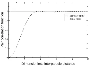
depends only on the separation of both electrons |r − r0|. Precisely, it takes the following form in 2D [11]: Fσ,σ0(r, r0) = N 2 4 − N 2δ σ,σ0 × " J1(kF|r − r0|) kF|r − r0| #2 , (2.8)
where J1 is the first order Bessel function of the first kind.
As shown in Fig. 2.1, if the spins σ and σ0 are different, the correlation function is a constant; but if the spins σ and σ0 are equal, the correlation function is an increasing function of the separation |r − r0| which is zero when r = r0: the mean separation between electrons with equal spins is larger than it is with different spins. In other words, the electrons with equal spins avoid each other as a consequence of the Pauli blocking6. Thus, the spin of the electron provokes a further repulsion on
top of the Coulombic repulsion, and each electron is surrounded by a finite area (in 2D) which is called the exchange hole. This hole acts as a net positive charge distribution whose attractive interaction with the electron reduces the total energy. This is the origin of the exchange hole energy term: Eexc = EpotHF.
0 2 4 6 8 10
Dimensionless interparticle distance 0 0.2 0.4 0.6 0.8 1
Pair correlation function
opposite spins equal spins
Figure 2.1: Pair correlation function for the two-dimensional electron plasma as a func-tion of the dimensionless interparticle distance kF|r − r0|.
The Hartree-Fock theory does not include Coulomb correlations which give rise
to the screening effect within the electron gas. These correlations lead to the so-called Coulomb hole which, as we shall see later in this chapter, has to be taken into account in the calculations. To treat these Coulomb correlation effects one has to go beyond the Hartree-Fock theory, using for instance the screened Hartree-Fock theory as we shall do.
Screened Coulomb potential
The phenomenon of screening is one of the most important manifestations of the many-body interactions in the electron plasma. The effect of the screening is to reduce the interaction range of the Coulomb potential as the plasma density in-creases. More specifically, the collective excitations in the electron plasma, also called plasmons, effectively reduce the strength of the Coulomb interaction, by in-creasing the value of the dielectric function with an inin-creasing plasma density at a given temperature.
Using the RPA and Poisson’s equation (see Appendix A), it is possible to show that the screened Coulomb potential seen by a test charge can be expressed as follows: Vs q = Vq ²q(ω) , (2.9)
²q(ω) being the dynamic dielectric function given by the Lindhard formula7: ²q(ω) = 1 − VqX
k
nk−q− nk
¯h(ω − iδ + εk−q − εk)
, (2.10)
where ¯hεkis the kinetic energy of an electron in a state k. The test charge has been assumed to be small enough so as to treat its effect on the plasma as a negligible perturbation; so, the quantity δ appearing in Eq. (2.10) indicates that this perturba-tion has been switched on adiabatically: the electron plasma was in a homogeneous state and its quasi-thermal equilibrium has always been maintained.
7In the electron hole picture, one needs to make explicit both the electron and the hole
which is a complex and retarded function: the poles are in the lower complex fre-quency plane. The Lindhard formula is valid both in three and two dimensions (no assumptions on the dimension of the potential have been made) and can describe both equilibrium and nonequilibrium situations8. Nevertheless, one needs to make
approximations to the Lindhard formula to obtain a simpler treatment of the plasma screening. One of the simplest situation which yields analytical results is when one uses the 2D static screening where ω − iδ −→ 0. Then one can modify the Lindhard formula using the static plasmon-pole approximation as shown in Appendix A (see also Refs. [45, 46, 11, 44], so as to obtain:
1 ²q = 1 − ω 2 pl(q) ω2 q . (2.11)
The quantities entering Eq. (2.11) are ωpl(q), the 2D plasma frequency9:
ωpl(q) = s e2n 2²m q = s 8πnR2 ya3B ¯h2 q, (2.12)
Ry and aB being the excitonic Rydberg energy and Bohr radius and ωq, the 2D effective plasmon frequency given by:
ω2q = ωpl2(q) µ 1 + q κ ¶ + νq2. (2.13)
In Eq. (2.13) the parameter κ is the 2D screening wavenumber which at equi-librium is given by:
κ = me 2 2π²¯h2 nk=0 = me2 2π²¯h2 ³ 1 − e−¯h2βπN/m´ (2.14) and ν2
q = C¯h2q4/16m2 is an additional term which simulates the contribution of the pair continuum; C being a numerical constant usually taken between 1 and 4
8For a thermal plasma, the particle density operator n
kfollows the Fermi-Dirac distribution.
9The plasma frequency is the eigenfrequency of the electron plasma density oscillations around
[11, 45]. For our purposes we shall always use the same value: C = 4.
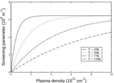
As mentioned earlier, the excitations in the electron plasma are responsible for the screening effect. This is reflected in Eqs. (2.9), (2.11), (2.12), (2.13) , and (2.14), showing that the strength of the Coulomb interaction within the electron gas heavily depends on its temperature and density.
0 2 4 6 8 10 Plasma density (1011 cm-2) 0 2 4 6 8 Screening parameter (10 8 m -1 ) T = 10K T = 30K T = 77K T = 150K
Figure 2.2: Screening parameter κ as function of plasma density, for various plasma temperatures, in a 2D ZnSe electron gas.
For a given temperature, the screening parameter κ, shown in Fig. 2.2 is an in-creasing function of the density n: the more electrons are present in the plasma, the less effective the Coulomb interaction between two charges is. However, for a given density, increasing the plasma temperature, weakens the screening effect. Consider-ing Eq. (2.14), the interplay between the carrier density and the plasma temperature becomes clearer if one regards the thermal wavelength, λ = 2π¯h2/mkBT , as the rel-evant physical quantity to discuss the plasma screening, as it gives a measure of the average spatial extent of the wave packets that represent the electrons in the plasma.
The 2D plasma frequency, as shown in Fig. 2.3, is a monotonically increasing function of the wavenumber q. From Eq. (2.12), one can also see the square root dependence of ωpl(q) on the plasma density. The higher the density, the faster the plasma density oscillates. From Eq. (2.13), one can see that for small values of q,
behaviour, i.e. a square root dependence on q. But as the wavenumber increases the continuum pair contributions becomes significant and ωq behaves like q2. With
increasing plasma density N, the parameter κ becomes larger, but that has a small effect on the density dependence of ωq as it is more influenced by the plasma fre-quency ωpl. 0 0.5 1 Wavenumber (109 m-1) 0 50 100 150 200 250 300
Plasma and plasmon frequencies (meV)
2D plasma frequency 2D effective plasmon frequency
N2 N1 N2 N1
Figure 2.3: Comparison of the 2D plasma frequency and the 2D effective plasmon fre-quency for two plasma densities, N1 = 1011 cm−2 and N2 = 1012 cm−2, in a 2D ZnSe
electron gas. The plasma temperature is T = 77 K.
2.2.2 Interacting electrons in a semiconductor quantum well
The above analysis of the properties of the electron gas will be helpful in describing those of semiconductor media in the Hartree-Fock approximation. But, as here one needs to take into account the specific band structure of these materials, the Hamiltonian of the interacting electron gas in Eq. (2.1) has to be modified: a band index is introduced and it is assumed that the excitation is achieved by optical pumping. Moreover, the finite well width of the quantum wells has a non-negligible effect on the optical spectra; so, modifications of the Coulomb potential will also be considered by introducing a form factor.
Semiconductor quantum wells
The need to improve the performance of the first semiconductor lasers (homostruc-ture devices) led to the design of semiconductor heterostruc(homostruc-tures which can be ob-tained with growth techniques such as molecular beam epitaxy with crystals that have sufficiently similar lattices. The reduced dimensionality leads to a more effi-cient population inversion of the confined electrons10as the allowed electronic energy
states and density of states are modified. With such type of structures the thresh-old current densities are lowered and one can obtain gain at room temperature and lasers operating cw.
As there is no quantum confinement in the xy plane one can define the total electron wavefunction ψn,k||(r) as the product of the two-dimensional free particle
eigenfunction φk||(r||) and ζn(z), solution of the Schr¨odinger equation including the
confinement potential Vconf(z). The vector r is defined by its transverse component r||(x, y) and the z component11, and the function φ
k||(r||) is given by: φk||(r||) = 1 √ A e (±ik.r||). (2.15)
The energy of the in plane motion is simply:
Exy = ¯h2k2
|| 2m||
. (2.16)
We obtain then a simple parabolic band structure. With w denoting the quan-tum well width, one can define the confinement potential as follows:
Vconf(z) = 0 |z| < w/2 Vc |z| > w/2 . (2.17)
In this case the ζn(z) is solution of the Schr¨odinger equation
10But the strength of the Coulomb interaction increases with lower dimensionality and affects
the efficiency of the population inversion process.
11In the same way one can distinguish between the effective masses m
−¯h2 d dz 1 mz d dz + Vconf(z) ζn(z) = Enζn(z). (2.18) Expression of the Hamiltonian in the two-band approximation
In general, semiconductors are characterized by a band structure consisting of one conduction band and several valence bands. These bands have asymmetric shapes and sometimes several energy extrema. The simplest model considers just two parabolic bands which most of the time is sufficient to describe some of the ba-sic behaviour of these materials as other completely filled bands do not contribute directly to the optical transitions of interest (visible region). In this chapter, we fo-cuse our attention first on such a two-band model before introducing the degenerate valence band. Furthermore, the following calculations are always based on parabolic band structures which is a good approximation as we consider only optical transi-tions with frequencies in the visible. These transitransi-tions are direct12 and therefore
we only need to consider a small region of the band structure around the bandgap minimum where they are most likely to occur and where the dispersion can be taken as parabolic.
The Hamiltonian of the electron gas in a semiconductor interacting with a ra-diation field ~E(r, t) can be written as follows [11]:
H = He+ HI (2.19) where He = X λ X k Eλ,ka†λ,kaλ,k+ 1 2 X λ,λ0 X k,k0 X q6=~0 Vq a†λ,k+qa†λ0,k0−qaλ0,k0aλ,k (2.20)
describes the dynamics of the electrons within the semiconductor, and
12The photon momentum is so small compared to the electron momenta involved in the optical
HI = − X λ,λ0 X k E(t)³dλλ0,k a†λ,kaλ0,k+ h.c. ´ (2.21) describes the interband dipole coupling to the light field ~E(r, t), dλλ0,k being the
pro-jection of the dipole moment dλλ0,kin the field direction ~E/E, and h.c. the Hermitian
conjugate. The wavevector k contains the spin index: (k, σ) ≡ k, unless otherwise stated. Apart from the inclusion of the interaction with the light field ~E(r, t), the main difference with the expression of the Hamiltonian given in Eq. (2.1) is the presence of the band index λ.
In the two-band approximation one deals with one conduction band λ = c and one valence band λ0 = v. These bands are taken as parabolic so d
λλ0,k does not
depend on the wavevector k. Thus, Eqs. (2.20) and (2.21) become:
He = X k ³ Ec,ka†c,kac,k+ Ev,ka†v,kav,k ´ +1 2 X k,k0 X q6=~0 Vq ³ a†c,k+qa†c,k0−qac,k0ac,k+ a†v,k+qa†v,k0−qav,k0av,k+ 2a†c,k+qa†v,k0−qav,k0ac,k ´ −X k E(t)³dcv a†c,kav,k+ h.c. ´ (2.22) Denoting Eg the unrenormalized bandgap (absence of excited electrons), the conduction and valence band energies are given by:
Ec,k = ¯h²c,k = Eg+ ¯h2k2/2mc, (2.23) and
Ev,k = ¯h²v,k = ¯h2k2/2mv, (2.24) using the single particle energies in the effective mass approximation. The effective masses are defined by the reciprocal of the band curvatures:
1 mi = 1 ¯h2 d Ei,k dk2 ¯ ¯ ¯ k=0 , i = c, v. (2.25)
The valence band having a negative dispersion, the effective mass as defined in Eq. (2.25) is negative.
Effects of a finite well width
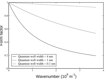
As mentioned earlier, the attention is mainly focused on 2D systems. However, real quantum wells have a finite width w and one has to deal with quasi-2D systems which still do not behave like 3D systems. It has been seen earlier that the dimensionality of the interacting electron gas has an effect on the strength of the Coulomb interaction: the confinement of the motion of the electron gas to a 2D space makes the Coulomb interaction stronger. The form factor fq characterizes the well-width-dependent deviations from the ideal 2D systems of V2D
q [44]: Vq = fq e2 2²A 1 q. (2.26)
The definition of the form factor fq and the calculations detailed in Appendix B give: fq = 2 w 1 q + 1 2 qw2 q2w2+ 4n2π2 + (e −qw − 1)1 w à 1 q − qw2 q2w2+ 4n2π2 !2 . (2.27)
The form factor fq is a finite, positive and monotonically decreasing function of
q. For q = 0 fq = 1, and limw→0fq = 1, which means that there is no alteration of
the 2D potential for a zero well width: one deals with the ideal 2D system.
With increasing the plasma density at a given temperature, the screening effect becomes important and we saw how we can quantify this effect in the section 2.1.3. But, at this stage, we did not deal with the more realistic situation of a finite well width. In the case of a screened Coulomb potential in a quasi-2D system, one has to alter the expression of the 2D plasma frequency and the 2D effective plasmon
frequency in Eqs. (2.12) and (2.13) so as to take into account the effect of the finite well width on the dielectric function, Eq. (2.11).
0 1 2 3 4 Wavenumber (109 m-1) 0 0.2 0.4 0.6 0.8 1 Form factor
Quantum well width = 4 nm Quantum well width = 1 nm Quantum well width = 0.1 nm
Figure 2.4: Form factor as a function of the wavenumber q for various well widths.
Using the calculations detailed in Appendix A together with the above definition of the Coulomb potential in a quantum-well, Eq. (2.26), yields:
ωpl(q) =
s
e2n
2²m fq q, (2.28)
for the quasi-2D plasma frequency, and
ωq2 = ω2pl(q) Ã 1 + q fq κ ! + νq2, (2.29)
for the quasi-2D effective plasmon frequency. The screening parameter κ is defined by Eq. (2.14).
With a finite well width the electrons are not strictly confined in an ideal 2D space. A direct effect is that the plasma density oscillations are slowed down for a given density. In other words, the 2D plasma frequency decreases with increasing the well width, which is coherent with Eq. (2.28) and the definition of the form factor.
Vs q = fqVq2D Ã 1 −ω 2 pl(q) ω2 q ! , (2.30)
in the static plasmon-pole approximation, with the quasi-2D plasma and effective plasmon frequencies defined as in Eqs. (2.28) and (2.29).
Quasi-Fermi levels in a semiconductor quantum well
When electrons in a semiconductor are excited, the fast carrier-carrier scattering drives the electron and hole nonthermal distributions into Fermi-Dirac distributions. As already briefly discussed in the Introduction this scattering mostly involves in-traband interactions. So, the equilibrium is only established within the bands and not amongst them: one does not deal with a proper thermodynamic equilibrium. Indeed, even if the time scale for quasi-equilibration is much longer than the in-traband carrier-carrier scattering time, it typically remains much shorter than the interband relaxation time. Nevertheless, one can define Fermi-Dirac distributions for each band characterized by a quasi-Fermi level, or chemical potential, µ. Obviously, as long as the electron system as a whole has not reached the thermodynamic equi-librium, these quasi-Fermi levels, evaluated with the same temperature and carrier density provided that the semiconductor is not doped, are not equal.
The Fermi-Dirac distribution is given by:
fk =
1
eβ (Ek−µ)+ 1, (2.31)
where Ek is the energy in the state k, and µ the chemical potential of the system. The total number of carriers, given by:
N =X
k,σ
fk, (2.32)
determines the chemical potential at a given temperature T . To evaluate the above expression we approximate the discrete sum by an integral. This requires the
knowl-edge of the free-particle density of states13, D(E). For quasi-2D systems like
semi-conductor quantum wells one can assume that taking the ideal 2D density of states is a good approximation, so Eq. (2.32) becomes:
N = N A = 1 2π Ã 2m ¯h2β ! Z ∞ 0 dE 1 eβ(E−µ)+ 1, (2.33)
After the evaluation of the integral in Eq. (2.33) one finds the expression of the 2D Fermion chemical potential as a function of the 2D carrier density N and the temperature T :
µ(N, T ) = 1
β ln
³
e¯h2βπN/m− 1´. (2.34)
This will be taken as the expression of the electron and heavy hole quasi-Fermi levels µe and µhh whose values also depend on the effective mass of the carrier me and mhh. 0 2 4 6 8 10 Plasma density (1011 cm-2) -100 -80 -60 -40 -20 0 20
Electron chemical potential (meV)
T = 10 K -- k BT = 0.86 meV T = 30 K -- k BT = 2.59 meV T = 77 K -- k BT = 6.64 meV T = 150 K -- k BT = 12.93 meV
Figure 2.5: Electron chemical potential as a function of plasma density for various tem-peratures.
The electron and heavy hole chemical potentials are an increasing function of the plasma density (see Fig. 2.5 for the electron chemical potential), but for a given density the higher the temperature is the lower the chemical potentials are. For a
13Even though we deal with an interacting electron gas, we assume that the free-carrier
the electron chemical potential as mhh > me. In the nondegenerate limit, i.e. low density and high temperature, the chemical potential diverges towards −∞.
2.3 The Semiconductor Bloch Equations
In very low excitation regimes, the Coulomb attraction between the conduction band electrons and the valence band holes is very important; however, no interactions between different electron-hole pairs have to be considered as the plasma density is low. But when the excitations become important, one has to deal with finite densities of carriers which are coupled dynamically to the interband polarization. The SBE give a realistic description of this coupling.
2.3.1 Hamiltonian equations
Definition of the interband polarization
The polarization P(t) is defined as the expectation value of the electric dipole er [11]: P(t) = X σ Z d3r h ˆψ† σ(r, t) er ˆψσ(r, t)i = X σ Z d3r Tr³ρ 0ψˆ†σ(r, t) er ˆψσ(r, t) ´ . (2.35) In Eq. (2.35):
• ρ0 is the density operator describing the system at the initial time before the
field was switched on.
• ˆψσ(r, t) is the electron field operator defined as: ˆ ψσ(r, t) = X λ X k aλ,k,σ(t) φλ,k,σ(r), (2.36)
where φλ,k,σ(r) is the single-particle eigenfunction for an electron in the semicon-ductor in the state specified by the band index λ, the momentum k and the spin
σ. In the case of spatially homogeneous system the eigenfunctions φλ,k,σ(r) are the Bloch functions as one is dealing with delocalized electrons. The operator aλ,k,σ(t) is the annihilation operator for the electron in that state. The notation h ˆOi stands for the expectation value of the operator ˆO calculated as:
h ˆOi = Tr ³ρ0Oˆ
´
. (2.37)
Inserting Eq. (2.36) into Eq. (2.35) yields:
P(t) = X σ X λ,λ0 X k,k0 ha†λ,k,σ(t) aλ0,k0,σ(t)i Z d3r φ† λ,k,σ(r) er φλ0,k0,σ(r). (2.38)
And writing the dipole matrix elements as:
Z d3r φ†λ,k,σ(r) er φλ0,k0,σ(r) = δkk0 dλλ0, (2.39) with λ 6= λ0, yields: P(t) =X σ X λ,λ0 X k ha†λ,k,σ(t) aλ0,k,σ(t)i dλ,λ0 = X σ X λ,λ0 X k Pλλ0,k,σ(t) dλ,λ0. (2.40)
This defines the interband polarization as:
Pλλ0,k,σ(t) = ha†λ,k,σ(t) aλ0,k,σ(t)i. (2.41)
The function Pλλ0 as defined in Eq. (2.41) would be zero in an equilibrium system
without a permanent dipole moment. However, the presence of the light field induces optical transitions between the bands; therefore, the interband polarization Pλλ0 in
Another possible representation of the problem is the electron-hole picture which is equivalent to the previous one provided that one defines the field operators for the electrons and the holes as follows [11, 44]:
β−k† = av,k α†k = a†c,k (2.42) Inserting the operators defined in Eq. (2.42) into Eq. (2.22) leads to the following expression for the Hamiltonian of the electron-hole gas interacting with a light field in the two-band approximation:
H =X k ³ Ee,kα†kαk+ Eh,kβ−k† β−k ´ +1 2 X k,k0 X q6=~0 Vq ³ α†k+qα†k0−qαk0αk+ βk+q† βk†0−qβk0βk− 2α†k+qβk†0−qβk0αk ´ −X k E(t)³dcv α†kβk† + h.c ´ , (2.43)
after restoring the normal ordering of the field operators using the anti-commutation rules and leaving out the constant terms.
In the electron-hole representation, the single particle energies given by Eqs. (2.23) and (2.24), become:
Ee,k = Ec,k = ¯h²e,k (2.44)
which remains unchanged, and:
Eh,k = −Ev,k+
X
q6=~0
Vq= ¯h²h,k (2.45)
which shows that the kinetic energy of the holes includes the Coulomb energy of the full valence band; or, in other words: the hole energy is the energy of the completely filled valence band minus the energy of the valence band with a vacant electronic
state. Eq. (2.45) shows a positive dispersion of the hole energy whereas Eq. (2.24) gives a negative dispersion for the valence band electrons: the effective hole mass mh and the effective valence band electron mass mv have opposite signs. Therefore, the effective electron mass me simply equals the effective conduction band electron mass mcand the hole effective mass, mh, is exactly the opposite of the valence band electron effective mass, mv. Note that the heavy hole dispersion in Eq. (2.45) takes the Coulomb interaction amongst the carriers into account and changes sign, but conserves the same curvature.
Derivation of the SBE
The quantities of interest are the electron distribution ne,k(t), the hole distribution nh,k(t) and the interband polarization pk(t) defined as:
ne,k(t) = hα†kαki nh,k(t) = hβ−k† β−ki pk(t) = hβ−kαki (2.46)
Based on these definitions and the Hamiltonian given by Eq. (2.43) we can derive the equation of motion for ne,k(t), nh,k(t) and pk(t), using the Heisenberg equation
of motion:
i¯h∂
∂t O(t) = [ ˆˆ O(t), H] (2.47)
for any operator ˆO(t) in the Heisenberg picture. Inserting the 2-operator products given in Eqs. (2.46) into Eq. (2.47), performing lengthy calculations involving the normal ordering of the Fermion operators, and taking the average defined as in Eq. (2.37) together with the definitions given in Eqs.(2.46) yields:
¯h " i∂ ∂t − (²e,k+ ²h,k) # pk = (ne,k+ nh,k− 1) dcv E(t) +X k0 X q6=~0 Vq ³ hα†k0−qβ−k−qαk0αki + hβk0+qβ−k−qβk†0αki (2.48) +hβk0α†k0−qαk0αk−qi + hβ−kβk0−qβk†0αk+qi ´ ,