HAL Id: tel-00904658
https://tel.archives-ouvertes.fr/tel-00904658
Submitted on 14 Nov 2013
HAL is a multi-disciplinary open access
archive for the deposit and dissemination of sci-entific research documents, whether they are pub-lished or not. The documents may come from teaching and research institutions in France or abroad, or from public or private research centers.
L’archive ouverte pluridisciplinaire HAL, est destinée au dépôt et à la diffusion de documents scientifiques de niveau recherche, publiés ou non, émanant des établissements d’enseignement et de recherche français ou étrangers, des laboratoires publics ou privés.
Taiping Zhang
To cite this version:
Taiping Zhang. Plasmonic-Photonic Hybrid Nanodevice. Other. Ecole Centrale de Lyon, 2012. English. �NNT : 2012ECDL0046�. �tel-00904658�
N° d‘ordre 2012-46 Année 2012
Thèse
Plasmonic-Photonic Hybrid Nanodevice
Présentée devantEcole Centrale de Lyon
Pour obtenir
Le grade de docteur
École doctorale : Electronique, Electrotechnique et Automatisme de Lyon
Par
Taiping Zhang
Soutenue le 22 novembre 2012 Jury ________________________________________________________________________ Rapporteur Rapporteur Examinateur Directeur de Thèse Co-directeur de Thèse Co-directeur de Thèse Thierry GROSJEAN David PEYRADE Natalia DEL FATTI Xavier LETARTRE Ali BELAROUCI Ségolène CALLARDChargé de Recherche CNRS Chercheur
Professeur des Universités Directeur de Recherche CNRS Chargé de recherche CNRS Professeur des Universités
Acknowledgment
This thesis has recevied numerous guidance and assistance from my advisors and colleagues at Institut des Nanotechnologies de Lyon. It would not have been possible without these individuals who contributed generously to the completion of this thesis.
I would first to give my deepest gratitude to my Directeurs de thèse: Xavier Letartre, Ali Belarouci, Ségolène Callard for giving me the opportunity of doing doctoral research under their supervision. I appreciate their continuing research advice throughout my PhD research. Their enthusiasm for science has set excellent examples and pushed me forward with great excitement and vitality.
Great appreciation goes to the colleagues who gave me many supports in technologies and theory during my thesis research: Cécile jamois, Céline Chevalier, Radoslaw Mazurczyk, Pedro Rojo-Romeo, Pierre Cremillieu, Jean-Louis Leclercq, Di Feng, Thanh-Phong Vo, Corrado Sciancalepore, Koku Kusiaku, Philippe Regreny, Brice Devif, Aziz Benamrouche, Regis Orobtchouk, Nicolas Chauvin, Pierre Viktorovitch, Michel Garrigues.
I would like to thank Prof. Natalia Del Fatti, Mr. Thierry Grosjean and Mr. David Peyrade as accepted to be my committee and for insightful comments and discussions. I would like to thank the colleagues who work at 4th floor of F7, Especially Thérèse Matin and Yves Robach for their kind helps. And same acknowledge to Nanophotonics group‘s members.
Last but not the least, I am grateful to my parents for their encouragement and blessing. You are the reason!
Contents
General Introduction ... 1
Bibliography... 4
Chapter 1: Research Background and Device Design ... 7
Introduction ... 8
1.1 Advances in the last 10 years and current status ... 9
1.1.1 Photonics ... 9
1.1.2 Plasmonics ... 11
1.1.3 Exploit Synergies between Plasmonics, Photonics, and Electronics .... 12
1.2 Basic building blocks of the hybrid device:... 13
1.2.1 Metallic nanostructures ... 13
1.2.2 Photonic element... 18
1.2.3 Hybrid Plasmonic-Photonic Crystal structure ... 24
1.3 FDTD simulation for the hybrid devices ... 44
1.3.1 FDTD simulation for the CL5 PC cavity without NA ... 44
1.3.2 FDTD simulation for the bowtie NA ... 45
1.3.3 FDTD simulation for the CL5 hybrid structures... 46
1.3.4 FDTD simulation for the CL7 hybrid structures... 48
Conclusion ... 49
Bibliography... 51
Chapter 2: Device Fabrication ... 57
Introduction ... 58
2.1 Epitaxial layer structure ... 59
2.2 Electron-beam lithography... 60
2.2.1 General description ... 60
2.2.2 Alignment issues and technique ... 62
2.2.3 Structure design... 63
2.4 Alignment marks fabrication... 68
2.6 Fabrication of NAs... 74
2.7 Fabrication results and discussion ... 75
2.7.1 Alignment accuracy... 75
2.7.2 The effects of SNOM tip ... 81
Conclusion ... 84
Bibliography... 85
Chapter 3: Optical Characterization in Far-Field for CL5 and CL7 Hybrid Structures ... 87
Introduction ... 88
3.1 CL5 and CL7 hybrid devices presentation... 88
3.2 Equipment set-up ... 91
3.3 Threshold and linewidth of the lasing emission measurement ... 92
3.3.1 Threshold of the lasing emission of CL7 and CL5 cavities without NA93 3.3.2 Threshold of the lasing emission CL7 and CL5 cavities with NA ... 96
3.3.3 Influence of the pumping power on the lasing wavelength ... 102
Conclusion ... 109
Bibliography... 110
Chapter 4: Optical Characterization in Near-Field for CL5 and CL7 Hybrid Structures ...111
Introduction ... 112
4.1 SNOM principle and set-up description ... 112
4.1.1 Illumination ... 114
4.1.2 SNOM scaning system... 115
4.1.3 Optical detection system ... 115
4.1.4 Near-field probes... 116
4.2 Near-field characterizations of S2-CL5 structures... 117
4.2.1 Spectroscopic results... 117
4.2.2 Far-field images of the laser mode... 122
4.3.1 Spectroscopic results of the CL7 structures ... 135
4.3.2 Far-field images of the laser mode... 137
4.3.3 Near-field maps of the CL7 structures ... 137
4.4 First step of investigation of the optical properties of graphite hybrid nanodevices ... 145
4.4.1 Far-field invistigation... 145
4.4.2 Near-field investigation... 146
Conclusion ... 148
Bibliography... 149
Conclusion and Perspectives ... 151
General Introduction
Many of the breakthroughs in human technology have resulted from a deeper understanding of the properties of materials. In the last few decades one goal in this case is to control the optical properties of materials [1]. The development of the nanotechnologies opens the way to artificial materials that allows for a tight control of the spatial- temporal trajectory of photons. This approach, the so-called light harnessing, leads to numerous functionalities: strong confinement or slow-down of
light, super prism phenomena… One of the most interesting possibility is to confine
the light within a tiny space (as compared to the wavelength) and for long time (as compared to the period), while achieving efficient light addressing (to), or collection (from) the wave-length scale photonic structures where they are meant to be confined. The general approach to achieve strong confinement of photons consists in high index contrast structuring of space at the wavelength scale. Materials commonly in use for that purpose are structured metals or high optical index dielectrics, immersed in low index dielectric material such as e.g. silica or air [2].
High index dielectric materials, such as semiconductors, have been widely used for photon confinement, along the so called refraction and Photonic Crystal (PC) based diffraction schemes: for the former, use is made of the total or partial internal reflection of photons at the semiconductor-low index material interface; for the latter, diffractive phenomena occurring in periodically structured materials are exploited to control the spatial-temporal trajectory of photons [2, 3].
On the other hand, metals have attracted considerable attention in the context of plasmonics: very strong spatial confinement of photons can be attained in plasmonic nano-structures, such as in metallic nano-particules or nanoantennas (NAs) [4, 5], at the expense however of a limited resonance strength (or confinement time) as a result of optical losses induced by metal absorption and of radiation to free space continuum. In recent years, we have witnessed a flurry of activity in the fundamental research and
development of surface plasmon based structures and devices [6]. Their unique properties enable a wide range of practical applications, including optical devices [7], optical energy transport [8], near field scanning optical microscopy [9, 10], surface-enhanced spectroscopies [11], and chemical and biological sensors [12].
Although it may seem that metallic nanoparticules (or optical antennas) are almost an off-the-self product, some issues need special attention and specific research. A key challenge is to address and collect light from those nano-scale systems. The tiny active area of the optical antenna is both an advantage for its miniaturization, and a real limit for the level of the collected signal. Therefore, one needs to reconsider how to drive efficiently such NAs. NAs are usually illuminated from the far field in a large, at best diffraction limited, focus. However, this procedure is not very efficient to address metallic micro- nano-structures or NAs. The reason lies in the difficulty to achieve a sufficient coupling rate between the incoming optical beam and the NA in order to compensate for the rather large optical losses (radiation to free space and metallic absorption). A new approach is proposed in the present work for the optimum addressing of NA with a free space optical beam via the use of an intermedia te coupling resonator structure, which is aimed at providing the appropriate modal conversion of the incoming beam, in the time domain [2, 13].
In this thesis, we propose to tackle this important issue by designing and realizing a novel nano-optical device based on the use of a photonic crystal (PC) structure to generate an efficient coupling between the external source and a NA. On one hand, the PC structure can take the place of intermediate coupling resonator structure to address the NA better. On the other hand, the NA can localize the optical field of the PC cavity in a very tiny space to create a subwavelength light source. Details of the PC-NA coupling analysis and its optimization were published elsewhere [13].
Some researches with similar kinds of plasmonic-photonic hybrid nanodevices were approached by other research groups [14, 15, 16, 17, 18, 19]. They had studied
range of applications. In our research, we expected to extend the study at the near- field level and to demonstrate a plasmonic-photonic crystal laser. This device may apply as a nano-laser source [20, 21, 22, 23].
In this dissertation, the content is arranged into three charpters. Chapter 1 introduces the theoritical background of this research including surface plasmon and photonic crystal concepts. This chapter also shows the design of the hybrid devices and demonstrates the numerical simulation of their optical properties. Chapter 2 mainly describes the process and the fabricated samples. The nanodevices are fabricated on an InP membrane substrate. The critical technology for the fabrication is complex electron beam lithography. With this technology the alignment of the positions of PC structure and NA is well controlled. Chapter 3 demonstrates the optical characterizations of the hybrid nanodevices including far- field characterizations and near-field characterizations. The far- field measurement is performed by micro-photoluminescence spectroscopy at room temperature. The results show that for the defect PC cavities, the presence of the NA influences the optical properties of the laser, such as lasing threshold and laser wavelength. The near- field measurement is performed by near-field scanning microscopy, at room temperature also. The investigation shows that the NA modifies the optical field distribution of the laser mode. The modification depends on the position and direction of the NA and it is sensitive to the polarization of the optical field.
Bibliography
[1] J.D. Joannopoulos, S.G. Johnson, J.N. Winn and R.D. Meade. Photonic Crystals: Molding the Flow of Light, 2nd Edn, (Princeton University Press).
[2] T. Zhang, A. Belarouci, S. Callard, P.R. Romeo, X. Letartre and P. Viktorovitch. Plasmonic-photonic hybrid nanodevice, International Journal of Nanoscience, 11(4) : 1240019 (2012).
[3] P. Viktorovitch, E. Drouard, M. Garrigues, J.L. Leclercq, X. Letartre, P.R. Romeo and C. Seassal. Photonic Crystals: basic concepts and devices, C. R. Physique, 8 : 253-266 (2007).
[4] S.A. Maier. Effective mode volume of nanoscale plasomn cavities, Optical and Quantum Electronics, 38 : 257-267 (2006).
[5] P. Mühlschlegel, H.-J. Eisler, O.J.F. Martin, B. Hecht and D.W. Pohl. Resonant Optical Antennas, Science, 308(5728) : 1607-1609 (2005)
[6] E. Ozbay. Plasmonics : Merging Photonics and Electronics at Nanoscale Dimensions, Science, 311(5758) : 189-193 (2006).
[7] Y. Dirix, C. Bastiaansen, W. Caseri and P. Smith. Oriented pearl-necklace arrays of metallic nanoparticals in polymers: A new route toward polarization-dependent color filters, Adv. Mater., 11 : 223-227 (1999).
[8] J.B. Pendry. Playing tricks with light, Science, 285 : 1687-1688 (2002).
[9] B. Knoll and F. Keilmann. Near-field probing of vibrational absorption for chemical microscopy, Nature, 399 : 134-137 (1999).
[10] B. Razavi. A 5.2-GHz CMOS receiver with 62-dB image rejection, IEEE J. Solid-State Circuits, 36(5) : 810-815 (2001).
[11] S. Nie and S.R. Emory. Probing Single Molecules and Single Nanoparticals by Surface-Enhanced Raman Scattering, Science, 277 : 1102-1106 (1997).
[12] R. Elghanian, J.J Storhoff, R.C. Mucic, R.L Letsinger and C.A. Mirkin. Selective Colorimetric Detection of Polynucleotides Based on the Distance-Dependent Optical Properties of Gold Nanoparticles, Science, 277(5329) : 1078-1081 (1997).
[13] A. Belarouci, T. Benyattou, X. Letartre and P. Viktorovitch. 3D light harnessing based on couping engineering between 1D-2D Photonic Crystal memberanes and metallic nano-antenna, Optics Express, 18(S3) : A381-A394 (2010).
[14] F. De Angelis, M. Patrini, G. Das, I. Maksymov, M. Galli, L. Businaro, L.C. Andreani and E. Di Fabrizio. A Hybrid Plasmonic-Photonic Nanodevice for Label-Free Detection of A Few Molecules, Nano Lett., 8 : 2321-2327 (2008).
[15] M. Barth, J. Stingl, J. Kouba, N. Nüsse, B. Löchel and O. Benson. A hybrid approach towards nanophotonic devices with enhanced functionality, Phys. Status Solidi B, 246(2) : 298-231 (2009).
[16] M. Barth, S. Schietinger, S. Fischer, J. Becker, N. Nüsse, T. Aichele, B. Löchel, C. Sönnichsen and O. Benson. Nanoassembled Plasmonic-Photonic Hybrid Cavity for Tailored Light-Matter Coupling, Nano Lett., 10 : 891-895 (2010).
[17] F. De Angelis, G. Das, P. Candeloro, M. Patrini, M. Galli, A. Bek, M. Lazzarino, I. Maksymov, C. Liberale, L.C. Andreani and E. Di Fabrizio. Nanoscale chemical mapping using three-dimensional adiabatic compression of surface plasmon polaritons, Nature Nanotechnology, 5 : 67-72 (2010).
[18] F.J. Gonzalez and J. Alda. Optical Nanoantennas Coupled to Photonic Crystal Cavities and Waveguides for Near-Field Sensing, IEEE Journal of Selected Topics in Quantum Electronics, 16(2) : 446-449 (2010).
[19] I.S. Maksymov. Optical switching and logic gates with hybrid plasmonic-photonic crystal nanobeam cavities, Physics Letters A, 375 : 918-921 (2011).
[20] R.F. Oulton, V.J. Sorger, T. Zentgraf, R-M. Ma, C. Gladden, L. Dai, G. Bartal and X. Zhang. Plasmon lasers at deep subwavelength scale, Nature, 461 : 629-632 (2009). [21] S-H. Kwon, J-H. Kang, C, Seassal, S-K. Kim, P. Regreny, Y-H. Lee, C. M. Lieber and H-G. Park. Subwavelength Plasmonic Lasing from a Semiconductor Nanodick with Sliver Nanopan Cavity, Nano Lett., 10 : 3679-3683 (2010).
[22] V.J. Sorger and X. Zhang. Spotlight on Plasmon Lasers, Science, 333 : 709-710 (2011).
[23] R-M. Ma, X. Yin, R.F. Oulton, V.J. Sorger and X. Zhang. Multiplexed and Electrically Modulated Plasmon Laser Circuit, Nano. Lett., 12(10) : 5396-5402 (2012).
Chapter 1: Research Background
and Device Design
Introduction
Photonics at the nanoscale, or nanophotonics might be defined as: the science and engineering of light- matter interactions that take place on wavelength and subwavelength scales where the physical, chemical, or structural nature of natura l or artificial nanostructure matter controls the interactions. Broadly speaking, over the next ten years nanophotonic structures and devices promise dramatic reductions in energies of device operation, densely integrated information systems with lower power dissipation, enhanced spatial resolution for imaging and patterning, and new sensors of increased sensitivity and specificity. Both photonics and plasmonics concern investigations into building, manipulating, and characterizing optically active nanostructures with a view to creating new capabilities in instrumentation for the nanoscale, chemical and biomedical sensing, information and communications technologies, enhanced solar cells and lighting, disease treatment, environmental remediation, and many other applications. Photonics and plasmonics share the characteristic that at least some of their basic concepts have been known for 40–50 years, but they have come into their own only in the last ten years, based on recent discoveries in nanoscience. Photonic materials and devices have played a pervasive role in communications, energy conversion, and sensing since the 1960s and 1970s.
Many of the critical concepts for today‘s rapidly growing and diverse field of
nanophotonics were established in past decades, but recent progress in the ability to control materials at the nanoscale in multiple dimensions has allowed the validation of those concepts and the anticipation of yet more intriguing and powerful photonic behaviors. For example, an early paper by Yablonovitch (1987) discussed dielectric materials with spatial variations in index of refraction on the order of a wavelength of light. He anticipated that these photonic crystals would have a dramatic effect on the spontaneous emission of light within these structures. Negative index materials, a component of a class of metamaterials, were anticipated as early as the 1960s by Veselago (1968). Surface plasmons have played an important role in surface-enhanced
Raman spectroscopy (SERS), an active area of research since the late 1λ70s. Today‘s research in plasmonics encompasses an even broader range of structures and applications, as is the case for photonics. Plasmonics aims to exploit the unique optical properties of metallic nanostructures to enable routing and active manipulation of light at the nanoscale. It has only been in the past 10 years that the young field of plasmonics has rapidly gained momentum, enabling exciting new fundamental science as well as groundbreaking real- life applications in the coming 10 years in terms of targeted medical therapy, ultrahigh-resolution imaging and patterning, and control of optical processes with extraordinary spatial and frequency precision. In addition, because plasmonics offers a natural integration compatibility with electronics and the speed of photonics, circuits and systems formed of plasmonic and electronic devices hold promise for next- generation systems that will incorporate the best qualities of both photonics and electronics for computation and communication at high speed, broad bandwidth, and low power dissipation.
1.1 Advances in the last 10 years and current status
1.1.1 Photonics
Over the last 5–10 years we have witnessed an enormous increase in the number and diversity of photonics applications. This has resulted from the significant advances in computational design tools and their accessibility, the emergence of new nanofabrication techniques, and the realization of new optical and structural characterization methods. At the forefront of these advances are the developments in the area of micro- and nano-photonic devices that have dimensions on the order of or below the wavelength of light.
Advances in electromagnetic and electronic device simulation tools have been tremendous over the last decade. Good co mmercial and freeware codes (e.g., finite difference time domain (FDTD), discrete dipole approximation (DDA), boundary element methods (BEM), or finite-difference frequency domain (FDFD) codes are
inexpensive and available to virtually everyone. Improvements in nanofabrication techniques, greater accessibility of high-resolution patterning (e.g., electron beam lithography), and pattern transfer processes (e.g., low-damage ion-assisted etching) have produced photonic crystal, microdisk, and ring resonator de vices with exceptional performance.
Discovery in nanophotonics has been enabled by the accessibility of optical nanoscale characterization tools such as scanning near-field optical microscopy (SNOM), atomic force microscopy (AFM), nano-Auger, nano-secondary ion mass spectrometry (nano-SIMS), scanning electron microscopes (SEMs), and transmission electron microscopes (TEM). These instruments have had a major impact on the ability to correlate the size, atomic structure, and spatial arrangements of nanostruct ure to the observed optical properties.
The progress in both simulation and fabrication of nanophotonic structures has resulted in the formation of ultrahigh-quality (Q, meaning low-optical- loss) optical structures [1]. These structures, in turn, have allowed researchers to engineer distinctive optical states, localize and slow the velocity of light, and create efficient light-emitting sources and strongly coupled light–matter interactions, resulting in new quantum mechanical states:
• Slowing of light has been observed in photonic crystal waveguides [2, 3] and in
coupled ring resonators [4]. This is an achievement not only scientifically, but also for the implication in controlled delay and storage of light in compact, on-chip information processing.
• Strong coupling between dielectric nanocavities and quantum dots has by now been
observed by a number of research groups [5, 6, 7]. The exciton-photon (polariton) states that result can form the basis of quantum information schemes, or produce ultra- low threshold lasers.
1.1.2 Plas monics
Although surface-enhanced Raman spectroscopy (SERS), one of the first ―killer
applications‖ of metallic nanostructures, was discovered in the 1λ70s [8, 9, 10], the young field of plasmonics only started to rapidly spread into new directions in the late 1990s and early 2000s. At that time it was demonstrated in rapid succession that metallic nanowires can guide light well below the seemingly unsurpassable diffraction limit [11], that metal films with nanoscale holes show extraordinarily high optical transmission [12], and that a simple thin film of metal can serve as an optical lens [13]. Plasmonic elements further gained importance as popular components of metamaterials, i.e., artificial optical materials with rationally designed geometries and arrangements of nanoscale building blocks. The burgeoning field of transformation optics elegantly demonstrates how such materials can facilitate unprecedented control over light [14].
As these novel phenomena captured the imagination of a broad audience, researchers in the lab started to also gain respect for some of the severe limitations of metals. The most important challenge that still persists today is that metals exhibit substantial resistive heating losses when they interact with light. For this reason, it will be valuable to explore ways to get around that issue. In some cases, local heat generation may be used to advantage, and in some cases heating losses can be neglected. A very diverse set of plasmonics applications has emerged in the last ten years. Early applications included the development of high-performance near-field optical microscopy (NSOM) and biosensing methods. More recently, many new technologies have emerged in which the use of plasmonics seems promising, including thermally assisted magnetic recording [15], thermal cancer treatment [16], catalysis and nanostructure growth [17], solar cells [18, 19], and computer chips [20, 21]. It now has been established that modulators and detectors can be achieved that meet the stringent power, speed, and materials requirements necessary to incorporate plasmonics with CMOS technology. Plasmonic sources capable of efficiently coupling quantum
emitters to a single, well-defined optical mode may first find applications in the field of quantum plasmonics and later in power-efficient chip-scale optical sources [22,23]. In this respect, the recent prediction [24] and realization [25, 26, 27] of coherent nanometallic light sources constitutes an extremely important development.
1.1.3 Exploit Synergies between Plasmonics, Photonics, and Electronics
Over the last decade, it has gradually become clear what role plasmonics can play in future device technologies and how it can complement electronics and conventional photonics. Each of these device technologies can perform unique functions that play to the strength of the key materials. The electrical properties of semiconductors enable the realization of truly nanoscale elements for computation and information storage; the high transparency of dielectrics (e.g., glass) facilitates information transport over long distances and at very high data rates. Unfortunately, semiconductor electronics is limited in speed by interconnect (RC) delay-time issues, and photonics is limited in size by the fundamental laws of diffraction. Plasmonics offers precisely what electronics and photonics do not have: the size of electronics and the speed of photonics. Plasmonic devices might therefore naturally interface with similar-speed photonic devices and with similar-size electronic components, increasing the synergy between these technologies. The assembly of hybrid nanophotonic devices from different fundamental photonic entities—such as single molecules, nanocrystals, semiconductor quantum dots, nanowires and metal nanoparticles—can yield functionalities that exceed those of the individual subunits. The next generation of challenges in the design and applications of nanophotonic circuits, fueled by the continuing development of powerful and flexible top-down and bottom- up nanofabrication techniques, lies in understanding and manipulating collective phenomena — phenomena that emerge from the interactions of the individual photonic, plasmonic, electronic and mechanical components. The scattering, radiative and mechanical properties of structures and materials dominated by collective phenomena can differ significantly from those of individual components. Additional
degrees of freedom offered by complex heterogeneous nanostructures can be used to obtain new device functionality through coupling- induced tailored control of fundamental physical processes.
Although merging these different systems on a single hybrid platform is at present challenging, it promises improved performance and novel devices. Particularly rapid progress is seen in the combination of plasmonic–dielectric constituents with quantum emitters that can be assembled on demand into fundamental model systems for future optical elements. Photonic and plasmonic nanostructures open up fascinating opportunities for controlling and harvesting light- matter interactions on the nanoscale. In particular, a capability of optical microcavities and plasmonic nanostructures to manipulate the local density of electromagnetic states could open up a variety of practical applications in optical communications and biomedical research. Properly-designed photonic and plasmonic nanostructures could also provide a useful testbed for the exploration of novel physical regimes in atomic physics and quantum optics.
In the scope of this thesis, we approach this technological relevant challenge by considering the design, fabrication and characterization of hybrid photonic–plasmonic devices that exploit the coupling between localized surface plasmon resonance (LSPR) of a bowtie antenna and a photonic mode provided by photonic crystal structures. In the next section the basic building blocks of the optoplasmonic structure will be highlighted.
1.2 Basic building blocks of the hybrid device:
1.2.1 Metallic nanostructures 1.2.1.1 The world of Plas mon
Many of the fundamental electronic properties of the solid state can be described by the concept of single electrons moving between an ion lattice. The motion of the electron gas in metals can be described by a classical equation of dynamics where the electron cloud follows a harmonic oscillatory behaviour. If we consider the metal as a three-dimensional crystal of positive ions and a free electron gas moving on the periodic potential created by the ions, when an electric or electromagnetic excitat ion is applied to the metal, the electron cloud will react to the corresponding electric field displacing from its equilibrium position. On the other hand, the positive ionic background induces a restoring force attracting the electron cloud back to its or iginal position. The action of those two forces will cause an oscillation of the electron gas at a frequency ωp around the equilibrium position:
e p m ne2 4 (1.1)
Where ωp refer to the volume or bulk plasma frequency, n is the electron density, and
me is the effective mass of the electron. The specific value of ωp for most metals lies
in the ultraviolet region, which is the reason why they are shiny and glittering in the visible spectrum. A light wave with ω< ωp is reflected, because the electrons in the
metal screen the light. On the other hand if ω> ωp the light wave gets transmitted (the
metal becomes transparent), since the electrons in the metal are too slow and cannot respond fast enough to screen the field.
1.2.1.2 Surface Plasmon Polaritons
Surface plasmon polaritons are similar to bulk plasmons however they are typically bound to and propagate along metal-dielectric interfaces. In this case, a combined excitation of free electrons i.e. a plasmon and a photon form a propagating mode bound to the metal-dielectric interface. A necessary condition for surface plasmon polaritons is that materials at the interface must have a Re(ε) of opposite sign. Metals, which are strongly absorbing, inherently have a Re(ε) < 0 and when interfaced to a
dielectric this condition is often met. Upon excitation of the surface plasmon polaritons, transverse and longitudinal electromagnetic fields propagate where a maximum intensity is present at the interface. Beyond and away from the interface, the field exhibits near-field or evanescent behavior with exponential decay from the interface (Figure 1.1). The frequency of surface plasma polaritons, ωsp is then:
2 p sp (1.2)
Figure 1.1: a) Schematics of SPP at an interface separating two semi infinite regions with two dielectric functions of different sign, propagating along x direction and confined in z direction. b) Energy (ω) versus momentum (k) dispersion line of the propagating surface plasmon polariton (blue-dashed line). The bulk plasma frequency
ωp and the surface plasmon energy ωsp = ωp/√2 are marked as dotted horizontal lines.
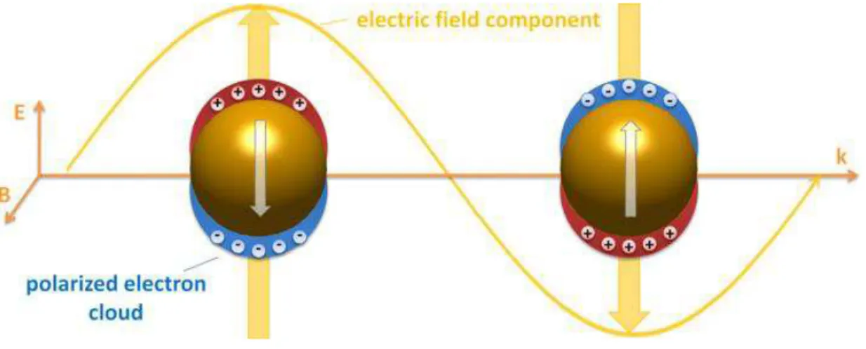
Figure 1.2: Excitation of particles plasmons through the polarization of metallic nanoparticles. At the resonance frequency the plasmons are oscillating with a 90° phase difference (180° above resonance).
In general, we have seen that plasmons arise from an interplay of electron density oscillations and the exciting electromagnetic fields. In this sense, we should talk about surface plasmon polaritons and also distinguish the propagating (evanescent) modes at the interface of a metal and a dielectric from their localized counterpart at the surface of metallic particles (so called particle plasmon polaritons). If an electromagnetic wave impinges on a metallic nanoparticle (whose spatial dimension is assumed to be much smaller than the wavelength of light), the electron gas gets polarized (polarization charges at the surface) and the arising restoring force again forms a plasmonic oscillation (Figure 1.2)
The metallic particle thus acts like an oscillator and the corresponding resonance behaviour determines the optical properties. Since we solely discuss particle plasmon polaritons in this work, we will furthermore always refer to them.
LSPs exhibit some distinct and special properties which have generated promising prospects in a variety of fields of science and technology. We summarize some of these properties:
• Localization of the electromagnetic fields: The fields induced by surface plasmons
decay exponentially as we move away from the interface where they are excited. Thus, all the electromagnetic effects induced by those fields are reduced to a small region close to the surface (typically some nanometers). Complementarily, plasmons have shorter wavelength compared to the incoming source that excites them. As a consequence of these two effects, it is possible to concentrate light on regions smaller than the diffraction limit. Thanks to this property, for example greater resolution can be achieved if plasmons are used for imaging purposes. On the other hand, this feature is also essential for spectroscopic applications where a small amount of molecules located near a surface can be sufficient for the detection purpose.
• Field enhancement: The plasmonic resonances induce charge pile up at the surface
of the metals and those charges induce electromagnetic fields on the surroundings of the surface. Therefore, the fields are enhanced compared to electro- magnetic fields in free space. This field enhancement is a key property for many photonic applications, such as spectroscopy and sensing.
• Tunability: Plasmons have also the capability of tuning the energy of their
resonances through the modification of both the geometry and/or the coupling between different systems [28, 29,30]. This opens up the door to engineer the optical spectral response in optically active systems to optimize the properties of plasmons for the requirements of a particular application. In addition, plasmons are extremely sensitive to the environment that surrounds them. Thus, a small change on the dielectric function of the surrounding medium can produce large spectral shifts on the far- field radiation of the system.
Such metallic nanostructures with specific length can act as efficient resonant antennas with strong potential for field enhancement schemes. Among diverse nanoantenna designs, closely placed particle pairs recently have attracted extensive research interest, and they are usually referred to as the nanoparticle dimmers. Early studies of the two interacting metal nanoparticles included a theoretical study in [31],
an experimental observation of gold spherical particles in [32] and systematic studies of separation distance of gold nanodisks in [33] and elliptical pairs in [34]. These studies of nanoparticle pairs were important because their coupling effect will lead to stronger field enhancement as well as much more effective confinement compared with a single particle [35, 36, 37]. In particular, obvious concentrations of luminance were observed near the sharp tips or inside the gap between the two particles of t hese dimmer nanoantennas [38]. The resonance can be further controllable by changing certain dimensional parameters and thus has potential engineering applications [39, 40]. The resonance's tuning characteristics depending on the gap are investigated in [41, 42]. Most intensively studied coupled particles structures include the bow-tie antenna, nanorods antenna and dipole antenna [38,43,44].
1.2.2 Photonic element
The general approach to achieve strong confinement of photons consists in structuring space with high index contrast at the wavelength scale, i.e. in the sub- micron range for the optical domain. Materials commonly used for this purpose are structured metals, including metal nano-particules, or high optical index dielectrics, immersed in low index dielectric material such as e.g. silica or air. We will concentrate on the later; the former being relevant to plasmonic has been described in the previous section.
The most commonly used high index dielectrics are semiconductor materials, including III-V compound semiconductors and silicon. For those materials, two confinement strategies are usually applied or combined:
- The refractive confinement scheme exploits the total or partial internal reflection of photons at the semiconductor-low index material interface. This strategy, widely used in traditional Optoelectronics, is principally devoted to devices operating solely in the waveguided regime. Strong confinement of optical modes can be achieved with this approach, owing to the high index contrast between the confining semiconductor micro-structures and the surrounding cladding material.
- The diffractive confinement strategy exploits diffractive phenomena in periodically structured materials to control the spatial-temporal trajectory of photons. This strategy is at the heart of quite a few of the recent developments in the field of Micro-Nanophonics, along the line of the Photonic Crystal (PC) approach. A photonic crystal, in which a periodic modulation of the index of refraction of a dielectric can guide light tightly and control its dispersion they are considered today as fundamental building block for the ultimate control of light in spatial and spectral domains (trapping of light in the photonic band gap regime, slowing down of photons in the slow Bloch mode regime). In the following, the basic concepts of photonic crystal will be reviewed.
1.2.2.1 Photonic crystal: a brief overview of basic concepts
A Photonic Crystal is a medium which the optical index shows a periodical modulation with a lattice constant on the order of the operation wavelength. The specificity of Photonic Crystals, inside the wider family of periodic photonic structures, lies in the high contrast of the periodic modulation: this specific feature is central for the control of the spatial-temporal trajectory of photons at the scale of their wavelength and of their periodic oscillation duration. Figure 1.3 shows schematic views of a variety of photonic crystals with dimensions ranging from 1 to 3.
One dimensional photonic crystals (1D PC) have been around for quite a long time in the very fertile field of thin film optics; however, the periodic structuration being limited to only one direction of space, de vices based on 1D PC suffer from a limited
angular resolution and their ‗lateral‘ size cannot be made compact. The concept of 3D
PC was demonstrated experimentally for the first time in the microwave regime. The initial motivation was the full control of the spontaneous emission of an active emitting material. 3D PCs are potentially the best candidates for this purpose and for many other applications, where the best control of photons in space and time is requested. However fabrication technology of 3D PC in the optical domain is extremely complex.
In between, 2D PCs are far more accessible than 3D PC, since they may be fabricated using planar technological schemes which are familiar to the world of integrated optics and micro-electronics. A real 2DPC consists in considering a 2D structuring of
a planar dielectric waveguide where photons are ―index guided‖, that is to stay
vertically confined by the vertical profile of the optical index. Figure 1.4 shows schematic and SEM views of a real typical 2DPC, consisting in a triangular lattice of holes formed in a semiconductor slab.
Figure 1.4: schematic and SEM views of a real 2DPC, consisting in a triangular lattice of holes formed in a semiconductor slab
In the rest of this chapter we will concentrate on the so called membrane approach, where the vertical confinement is achieved in a high index semiconductor membrane surrounded with low index cladding or barrier layers (for example an insulator like silica or simply air).
1.2.2.2 Optical mode confinement schemes in 2D PC me mbranes
The principal characteristics of the photonic crystal manifest themselves in the so called dispersion characteristics of the periodically structured medium, which relate the pulsation ω (eigen value) to the propagation constants k (eigen vector) of optical modes, and which are the eigen solutions of Maxwell equations, corresponding to a stationary spatial distribution of the electromagnetic field. It is appropriate here to speak in terms of dispersion surfaces (k)= (kx, ky), real space being
two-dimensional. Strong diffraction coupling between optical modes occurs; these diffraction processes affect significantly the surface dispersion characteristics, or the so called band structure, according to the solid state physics terminology. The essential manifestations of these disturbances consist in (see Figure 1.5) the opening of multidirectional and large photonic band gaps (PBG):
- The opening of multidirectional and large photonic band gaps (PBG)
- The presence of flat photonic band edge extremes (PBE), where the group velocity vanishes, with low curvature (second derivative)
PBG 1
Figure 1.5: schematic representation of a photonic band gap (PBG) and of related photonic band edges (PBE) in the dispersion characteristics of a photonic crystal.
PBG confinement scheme using localized “defect” or cavity modes
In the PBG scheme, the propagation of photons is forbidden at least in certain directions. This is in particular true when they are trapped in a so called localized defect or microcavity and the related optical modes are localized: in this case the propagation of photons is fully prohibited. Opening of large PBG (in the spectral range) provided by the PC, allows for a very efficient trapping of photons, which can be made strongly localized in free space. The basic building blocks of photonic components for in plane operation along the PBG scheme are micro-cavities [45] and waveguides [46]. These building blocks were among the earliest structures based on 2DPC reported in the field: they have been the matter of a large number of publications since the late nineteen nineties and have resulted in the production of a variety of devices including very high Q factor nanoreso nators for Quantum Electrodynamics [47], very low loss wave- guides [48], micro- lasers [49], channel drop filters [50], etc…
PBE confinement scheme using delocalized slow Bloch modes
In the PBE scheme, the PC operates around an extreme of the dispersion characteristics where the group velocity of photons vanishes. It is more appropriate to
periodical structure): it can be shown that the lateral extension of the area S of the slowing down Bloch mode during its lifetime τ is proportional to ατ [51]. As mentioned above, one essential virtue of PC is to achieve a very low curvature α at the band edge extremes, thus resulting in strong slowing down and a very efficient PBE confinement of photons. Although the PBE scheme provides weaker confinement efficiency than with the PBG approach, it results in an improved control over the directionality or spatial/angular resolution of the light. Active as well as passive devices have been demonstrated. For the former, Bloch mode micro-lasers designed for in-plane emission have been reported (see, for example [52, 53]). Passive structures as channel drop filters making use of the PBE scheme have also been proposed: the principal advantage over their counterpart based on the PBG scheme, lies in their ‗natural‘ propensity to provide a directional dropping [54, 55].
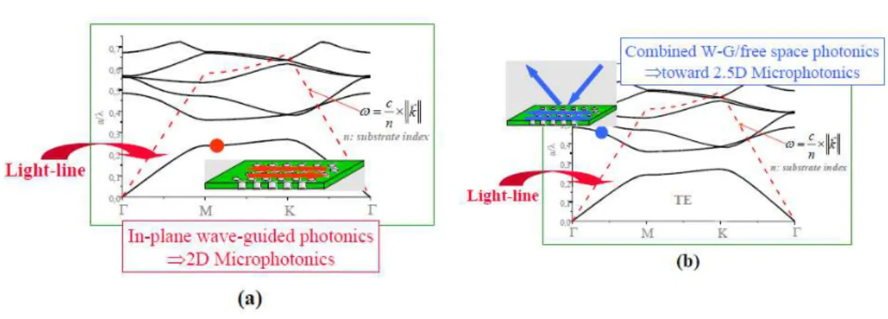
The issue of vertical confinement in 2DPC: below and above light-line operation
It has been explained previously that the vertical confinement of photons is based on refraction phenomena. However, full confinement of photons in the membrane wave-guiding slab is achieved only for those optical modes which operate below the light- line (see figure 1.6a). This mode of operation is restricted to devices which are meant to work in the sole wave-guided regime, where wave-guided modes are not allowed to interact or couple with radiative modes. For waveguided modes with dispersion characteristics lying above the light line, coupling with the radiated modes
is made possible, the waveguided ‗state‘ of the related photons is transitory, and the
photonic structure can operate in both waveguided and free space regimes (see figure 1.6b).
Figure 1.6: below (a) and above (b) light-line operation of photonic structures based on 2D photonic crystals
1.2.3 Hybrid Plas monic-Photonic Crystal structure
Hybrid resonant metallo-dielectric structures allow combining the best of two worlds: multiple- frequency and high-Q properties of photonic components with the nanoscale dimensions of plasmons, leading to a wealth of novel effects. In particular, interaction of high-Q photonic modes with the localized SP resonances on noble- metal nanostructures results in giant cascaded field enhancements within subwavelength volumes in hybrid optoplasmonic devices. Enhanced information and energy transfer in optoplasmonic materials due to greatly reduced dissipative losses when compared to plasmonic waveguides is only one example where hybrid plasmonic-photonic crystal creates new functionalities beyond the capabilities of the individual building blocks. We anticipate that optoplasmonic components will also facilitate active nanoplasmonic circuit elements for field modulation and frequency switching, as photon recycling in microcavities; translates into narrow linewidths and thus greatly enhances mode sensitivities to external stimuli and environmental changes.
In the following I will place a particular emphasis on a model system combining a metallic nanoantenna and a dielectric photonic crystal to efficiently collect radiatio n over an extended area and funnel it into a single well-defined nanoscale focal spot.
Ultimate spatial confinement of photons can be attained in plasmonic nano-structures, such as in metallic nano-particules or nano-antennas (NA), at the expanse however of a limited resonance strength (or confinement time) as a result of optical losses induced by metal absorption and of radiation to free space continuum. However, excitation of individual plasmonic NA using free-space optics is not efficient, and the signal-to-noise-ratio is very small. The reason lies in the difficulty to achieve a sufficient coupling rate between the incoming optical beam and the NA in order to compensate for the rather large optica l losses (radiation to free space and metallic absorption) [56]. It has been shown that a darkfield microscope can be used to interrogate individual plasmonic nanoresonators by using scattering spectroscopy [57]. This still requires a very sensitive detector and a bulky microscope system with a precise alignment control. The inefficient coupling of the lightwave to each individual plasmonic nanoresonator reduces the signal-to-noise-ratio in sensing and spectroscopy applications; and it also limits the level of possible field enhancement, which is necessary for efficient light- matter interaction. To harness the advantages of plasmonic antenna for practical applications, it is essential to improve the coupling of the lightwave to the localized surface plasmon resonance modes.
A new approach is proposed in the present work for the optimum addressing of NA with a free space optical beam via the use of an intermediate coupling resonator structure, which is aimed at providing the appropriate modal conversion of the incoming beam, in the time domain. The basic idea consists in relaxing the stringency of the coupling conditions by increasing the optical energy density achieved in the vicinity of the NA, owing to the photon storage capabilities of the intermediate resonator. More specifically, the intermediate resonator is a PC membrane resonant structure based on surface addressable slow Bloch modes. Those structures are currently recognized as very versatile photonic platform in a sense that there are not only restricted to operate in the in plane wave-guiding regime, but can be opened to the third space dimension by controlling the coupling between wave-guided and radiation modes. They have the capability to provide the optimum conversion of the
incoming free space optical beam into a wave- guided slow Bloch mode with spatial and temporal confinement characteristics accurately designed to achieve the finest coupling conditions to metallic NA.
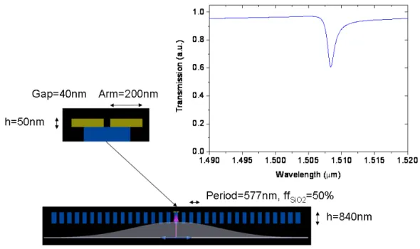
We consider here a 1D PC membrane which consists in a periodic array of low index material slits (silica) formed in a high index silicon membrane. The structure, which is designed in order to accommodate a slow Bloch mode Fano resonance, with a large quality factor, addressable in the vertical direction, is shown in Figure 1.7, where its topological parameters (membrane thickness, period and silica filling factor of the slit array) are given. The transmission spectrum obtained by 2D FDTD simulation (here we assume that the size of the structure along the slit direction is infinite w ith respect to the wavelength) is also reported and reveals a resonance near 1.506 m. The lateral size of the incoming excitation beam is 12 m and its polarization is TM (electric field perpendicular to the slits: blue arrow in Figure 1.7).
Figure 1.7: Schematic view of the 1D PC membrane reflector used as an intermediate coupling resonator. (The topological parameters of the structure are given in the figure). The field intensity distribution at resonance and the transmission spectrum are also shown.
The strength of the resonance is given by the spectrum bandwidth which is related to its quality factor,QPC c
0 0
, where 0 is the Fano resonance wavelength.
QPC is around 4800, which corresponds to a rather strong resonance. The reflectivity
of the structure is close to 100% at the resonance wavelength: this indicates that the above discussed optimum coupling, or impedance matching, conditions between the incoming optical beam and the wave-guided slow Bloch mode are achieved (in-plane k-vector and lateral size matching). The field intensity distribution of the Fano resonance is also reported.
Let‘s consider now the coupling scheme to the NA based on the use of the
intermediate PC membrane resonator, as shown in Figure 1.8. The NA is a gold dipole which has been designed to match the wavelength of the PC resonator with the following geometrical parameters: 50nm thickness, 200nm arm length and 40nm feed gap width. The gold dielectric function was obtained by fitting on the optical bulk
experimental data reported in [58], for the frequency of interest. Other metals (eg silver) could have been chosen as well to illustrate the proposed coupling scheme. The PC membrane is addressed with a Gaussian optical beam (diameter 12 m) from the bottom and the NA is located above the membrane at a variable distance, which results in a variable coupling time constant τ between the NA and the PC membrane resonator: the topological parameters of the structure are given in the figure. An example of transmission spectrum of the system is also shown (NA put directly on top of the PC membrane): the narrow Fano resonance response shows up within the much wider background of the NA spectral response, which cannot be made visible in the narrow wavelength range of the spectrum. This is a clear indication that indeed, the PC membrane resonance is much stronger than the one of the NA
Figure 1.8: Schematic view of the 1D PC membrane reflector used as an intermediate coupling resonator. (Topological parameters of the structure are given in the figure). The transmission spectrum is also shown.
A plot of the maximum electric field intensity in the NA as a function of the distance between the latter and the PC membrane is shown in Figure 1.9, at the resonance wavelength (1.51 m). As expected from coupled mode theory, the electric field
distance between the NA and the PC membrane resonator. The field intensity distributions of the structure are also shown in Figure 1.9. The gloss of the NA reaches its maximum under the optimum coupling conditions. For decreasing coupling rates, that is for increasing coupling distances, the NA darkens to the PC membrane advantage, which brightness increases gradually, before levelling off at a saturation value.
Figure 1.9: Plot of the maximum electric field in the NA as a function of the distance between the latter and the PC membrane. The field intensity distributions in the structure at resonance are also shown.
For sake of comparison, we have carried out FDTD simulations of the direct addressing of the NA, positioned at the waist of a focused optical beam under the diffraction limit conditions (waist size down to 1.5 m): the optimum coupling conditions could not be attained; the maximum field intensity (normalized to the total input optical power) achievable in the NA was a factor 3 below the one achieved with
the help of the PC membrane, which does not require light focusing. This comparison is illustrated in Figure 1.10, where the electric field intensity distributions are shown for direct addressing and PC membrane mediated addressing of the NA, respectively: for the case of direct addressing, the field colour scale intensity has been artificially multiplied by a factor of 3, in order to make clearly visible (i) the focused incoming free space beam and (ii) the factor 3 enhancement of the maximum achievable electric field intensity in the NA, with the help of the PC membrane.
Figure 1.10: Field intensity distributions at resonance for a NA directly addressed by a focused Gaussian beam (left) and PC membrane mediated addressing of the NA (right).
In the previous section, a generic approach for 3D light harnessing based on the coupling engineering between Photonic Crystal membranes and metallic optical antenna has been discussed. No only does this approach allow for very efficient light insertion in tiny micro-nano-resonator structures, but also it opens the way to the production of a wide range of functionality. In the present contribution, this approach is illustrated with the demonstration of efficient light addressing of low quality factor and very high Purcell factor metallic NA; it can be fruitfully extended to the addressing of high quality factor micro-nano-resonators, thus widening the range of accessible coupling regimes, including the strong coupling regime. Attractive
strong light concentration and/or accurate beam shaping is requested with sub-wavelength spatial resolution: they include low optical power consuming non- linear optics, sensing and bio-photonics, highly sensitive resonant near- field spectroscopy and imaging, light trapping with sub-wavelength spatial resolution, etc…
In the next section we will highlight the design of hybrid plasmonic-photonic structures combining a metallic bowtie antenna with:
- A slow Bloch mode PC. As discussed formerly they can be used to address one or several NA from free space, improving the signal- to-noise ratio and the field enhancement
- A defect state based PC. The ability to confine light into ultrasmall volumes is
essential for enhancing the interaction of light and matter in the emerging field of nanophotonics. Surface plasmons provide a route to such strong optical confinement in the subwavelength regime and are of high interest for (cavity) quantum electrodynamics applications. Because of their ability to concentrate electromagnetic energy in volumes much smaller than the corresponding wavelength, they provide a very strong interaction between (quantum) emitters and photon fields. However, plasmonic cavity Q factors have so far been limited to values less than 100 both for visible and near- infrared wavelengths [59,60,61]. An optoplasmonic structure can thus exploit this field compression exhibiting both high quality factors and pronounced hot spot of the electromagnetic field, potentially enhancing the interaction of the cavity mode with emitters or other types of active materials.
1.2.3.2 The antenna design
Optical and infrared antennas based on metal nanostructures allow for efficient conversion of propagating light into nanoscale confined and strongly enhanced optical
fields, and vice versa. This special capability enables a variety o f cuttingedge applications. In order to maximize the benefits of optical antennas it is necessary to tailor them in order to satisfy the specific needs of each application. In that sense, the control over the localization of the areas where the near-field is maximum (hot-spots) and the tuning of the resonant frequencies of the antennas are central to reach the best optical coupling condition with the PC structure. Bowtie nanoantennas have attracted much attention in the scope of nano-optics [62, 63, 64]. It consists of two opposing tip-to-tip metal triangles, separated by a small gap (see figure 1.11). The sharp corner of each arm leads to strong charge concentration at the edge of each triangle inside the gap. Moreover, localization of fields inside the gap is more likely to increase while two sharp edges with opposite charges are closely spaced [65]. Similar to a dipole antenna, the ratio between the physical length and the incident wavelength determines their impedance. The impedance of a bowtie antenna with large α can be denoted as broad-band impedance, which make them useful for a larger frequency range [66]. Experimental observations on bowtie antennas show that the resonance peak is dramatically influenced by the gap size [64].
influenced, when an antenna is scaled to the optical regime. At optical frequencies metals are no longer perfect conductors and the assumption made by classical antenna theory, that e.m. fields are restricted to the outside of an antenna is no longer valid. Depending on the permittivity of the antenna material the fields penetrate the surface in an extent given by the skin depth. At optical frequencies the skin depth for many metals is quite large and is, even for thick antennas, comparable with the antenna diameter. Seeing the antenna as e.m. boundary problem, the large skin depth at optical frequencies increases the complexity of the problem. The current distribution and hence the antenna input impedance of optical antennas will differ to some degree from the predictions made by classical antenna theory. This will affect the resonance length as well as the achievable field enhancement in the feed gap o f an OA. The presence of a substrate also modifies the position of the resonances. To predict in more detail the function of an OA one has to perform computer simulations that take into account the antenna shape and the finite and frequency dependant permittivity of the antenna material. To perform the design and to support the interpretation of the experimental data a commercial software (LUMERICAL) based on the finite-time-domain (FDTD) method has been used. The method requires that at least the structure itself is
discretized in a computational grid. The grid size (dx; dy; dz ≤ /(50n)) must be small
compared to the wavelength and smaller than the smallest feature in the computation volume. Structures with very fine details require a larger computational domain, resulting in much longer solution times.
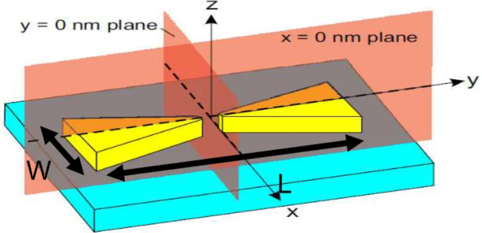
We performed FDTD simulations for a gold bowtie geometry on a flat InP substrate. The bowtie geometry (W=140nm, L =270nm, height= 40 nm, feed gap size=20 nm) chosen for the simulation has been optimized to ho ld a plasmonic resonance exactly matching the spectral position of the photonic mode. A sketch of the geometry used for the simulation is shown in Figure 1.12. The dielectric function for gold, titanium adhesion layer, and InP was given by the simulation software. The discretization cells were chosen to be 3x3x3nm3 cubes. Exemplarily two monitor planes (x = 0 nm and y = 0 nm) are indicated. The bowtie is addressed with a plane wave coming from the
substrate and polarized in the y or x direction.
Figure 1.12.: Sketch of bowtie geometry. Bowtie dimensions used for FDTD simulations, W=140nm, L=270nm, gap=20nm, height =40nm.
The near- field intensity enhancement factor ( E/ E0 2) 10 nm above the antenna as a function of wavelength is reported on Figure 1.13. The plane wave is polarized in the y-direction (see Figure 1.12) and E0 refers to the incident evanescent field in the
absence of the antenna.
Figure 1.13.: Near-field intensity enhancement factor versus wavelength
There is a very large field enhancement (over 400) around 1.5µm corresponding to the x-polarization. The spectrum is broad and the quality factor of the resonance is estimated to be close to unity.
To understand the field confinement and enhancement in bowties a theoretical simulation was done to model the electromagnetic field enhancements in the different polarization directions as shown in Figure 1.14. The y-direction polarization enhances the field in the center of the bowtie gap while y-direction exhibits strong enhancement along the outside tips of the bowtie. The enhancement is about 1000 when the bowtie is launch with a polarization along y and 100 in the perpendicular direction.
Figure 1.14 Near-field intensity mapping ( E/ E0 2 ) of the bowtie antenna with incident polarization in the y-direction (a and b) et the x-direction (c and d)
1.2.3.3 Slow Bloch mode based PC design
In this part, we theoretically study the electromagnetic properties of a PC microcavity supporting a slow Bloch Mode (SBM) located at the Γ-point in the first Brillouin zone. The choice of this configuration is motivated by two main reasons:
- The k-space localization of the mode is exploited to get directive vertical emitting devices.
cavity size
As a basic structure to build the slow light resonator, we use a InP-based 2D PC slab that consists of a regular array of air holes, drilled in a membrane, and which exhibits
a slow light mode around =1.5µm. In the remainder of this thesis, we will consider a
honeycomb (graphite) 2D PC structure for several reasons. (i) Compared to a triangular or a square lattice, the surface filling factor of the semiconductor is higher for a honeycomb structure which makes it ea sier to position the NA in the nanofabrication process. In an active structure a majority of emitters (qdot or qwell) will be located far from the hole interfaces, reducing the effect of surface recombination (ii) The honeycomb structure exhibits several flat bands at the Γ-point. Photons in such modes exhibit a low group velocity and the lateral light confinement is then improved. Active 2D PCs were designed to support band-edge modes at the
Γ-point of the first Brillouin zone. The structure consisted of a 240nm-thick
monomode slad InP (n=3.17 at =1.55 m) bonded on SiO2 transparent substrate. At
the center of the InP slab, four quantum wells of InAsP separated by InP barriers (see
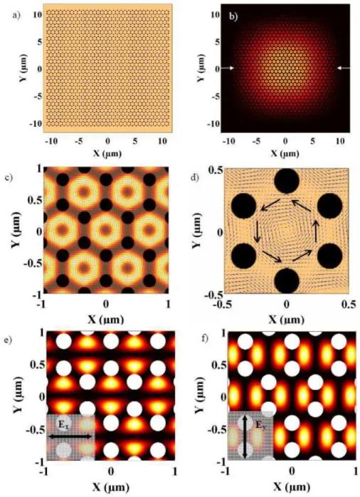
Figure 1.15) were embedded to provide internal photoluminescence from 1.3 m to 1.65 m. An array of honeycomb- like cylindrical air holes (e=1) was drilled on InP slab (Figure 1.15-a/b) to provide the periodical dielectric structure with a high contrast of refractive index. The two basic parameters of the honeycomb PC are the lattice parameter a (center-to-center distance of two nearest hexagons) and the hole radius (r). The surface air filling factor was calculated from the following formula:
2 3 4 a r ff 1.3
Figure 1.15: Model of defect–free honeycomb 2D PC. a) (Top view). An array of cylinder air holes (white circles, e=1) centred at the vertex of periodically arranged hexagons on InP slab (grey area, e=10 at =1.55 m). b) (Top view) SEM image of a typical 2D-PC. Real lattice parameters measured a=730nm, 2r=245nm, then corresponding ffair=0.2. c) (Side view). Sample includes 240 nm thick InP slab bonded
on top of a SiO2 transparent substrate with four layers of InAsP quantum wells (separated by InP barrier) are embedded at the center of the InP slab. d) The first Brillouin zone with high-symmetry points (Γ-K-M) in the reciprocal space with respect to the real space unit cell.
The Plane Wave Expansion method (PWE) developed by the MIT [67] has been used to determine the band diagram of the PC structure. It is a well known method in frequency-domain that allows extraction of the Bloch wave functions and frequencies by direct diagonalization.
Figure 1.16: Band diagram (TE polarization) of the graphite 2D PC (dashed line: light line), z-component of the magnetic field and intensity distributions of several
Γ-point modes.
Figure 1.16 shows typical map of the z-component of the magnetic field Hz and
electric field intensity map of the different Γ-point band-edge modes. We consider even modes (TE- like modes), with respect to a mirror plane located in the centre of the slab. To get a large β- factor, we must ensure that the emitters couple to only one resonant mode. Accordingly, the Γ-point Bloch mode must be non-degenerate and sufficiently spectrally isolated from the other slow Bloch modes. We see in figure 1.16 that two modes satisfy this requirement: the monopolar and hexapolar modes. The spatial distribution intensity of the monopolar mode is mainly located in the material as compared to the intensity of the hexapolar mode: 82% of the intensity is in the InP material. This promotes the interaction of the modes with the emitters and also relaxes the constraint of positioning the NA on the backbone of the PC lattice.
A PC lattice parameter A = 730nm is determined so as to operate around ~1.5µm. This corresponds to a distance between the closest holes of 240nm. An air filling factor of ff = 20% selected and results from a balance between 2 criteria: (i) to ensure a good spectral isolation of the monopolar mode with respect to other Γ- point slow Bloch modes; (ii) to keep reasonable technological constraints.