Development of Ultra-Broadband
Modulators
byOrit A. Shamir
B.S. Electrical Engineering MASSACHUSETTS INSTITUTE OF TECHG;LO2GYNOV 1
3
2008
I-Massachusetts Institute of Technology, 2007
Submitted to the Department of Electrical Engineering and Computer Science in partial fulfillment of the requirements for the degree of
Master of Engineering in Electrical Engineering and Computer
Science
at the
MASSACHUSETTS INSTITUTE OF TECHNOLOGY June 2008
@
Massachusetts Institute of Technology 2008. All rights reserved.A uthor ...
Orit A. Shamir Department of Electrical Engineering and Computer Science May 23, 2008 Certified by..
S J
Leslie A. Kolodziejski
Professor of Electrical
" ..
Engineering and Computer Science
'7
, ,,y
Thesis Supervisor
Accepted by...
Arthur C. Smith
Chair, Department Committee on Graduate Students
ARCHIVES
a5 &IJ ~171 ~\1 ~hJ i
Development of Ultra-Broadband Modulators
byOrit A. Shamir
Submitted to the Department of Electrical Engineering and Computer Science on May 23, 2008, in partial fulfillment of the
requirements for the degree of
Master of Engineering in Electrical Engineering and Computer Science
Abstract
Optical signal modulation is a cornerstone of communication, allowing the transfer of information by electrically encoding data onto an optical carrier. Modulation with ultra-broadband capability enables the generation of arbitrary waveforms using the electro-optic effect. By separating an incoming pulsed optical source into a frequency comb through the use of arrayed waveguide gratings, and employing both phase and amplitude modulation using Mach Zehnder Interferometers, an arbitrary waveform is constructed following frequency channel recombination.
Modulation of frequency combs centered at an operational frequency of 800nm re-quires the use of GaAs-based and InP-based materials that are transparent at 800nm. The design and growth of III-V structures, the fabrication of ultra-broadband modu-lators and the design of arrayed waveguide gratings are detailed in this work. Three distinct structures are presented along with a compatible fabrication procedure for the construction of discrete modulators. The work is culminated with a discussion of further steps in the realization of an optical arbitrary waveform generating system. Thesis Supervisor: Leslie A. Kolodziejski
Acknowledgments
It only seems fitting that this thesis begins with the opportunity to thank all who have supported me and helped me push through the best and the worst of times.
My incredible advisor, Professor Leslie Kolodziejski, has given me the greatest of opportunities in making me part of her group. Her guidance and high spirits kept me grounded and focused, and her humor always provided relief from the daily stress. What I have learned from her extends far beyond the laboratory or classroom, and I cherish the experiences she has afforded me over the last two years.
Dr. Gale Petrich is truly one of the greatest resources at MIT. A day has yet to go by when I do not have a question to run by him, and the answers have always been more than helpful. I thank him for all the knowledge he has imparted to me, and for his generosity both in and out of the lab.
I would like to thank all who are involved in the Optical Arbitrary Waveform Gen-eration project: Marcus Dahlem, Ali Motamedi, Dave Chao, Jason Sickler, Jeff Chen, Jonathan Morse, Michelle Sander, Professor Erich Ippen, Professor Franz Kaertner, and all others who are involved directly or indirectly. I am excited to be part of this effort and am looking forward to what the future (and a lot of hard work) will bring.
This work would not have been possible without my colleagues in the Nanostruc-tures Laboratory (NSL) and the Microsystems Technology Laboratory (MTL). I want to thank Professors Henry Smith and Karl Berggren for granting me access to their laboratory as well as to their students, including but certainly not limited to Amil Pa-tel, Trey Holzwarth, Euclid Moon, Bryan Cord, Sidney Tsai, Joel Yang, and Donald Winston, who are always willing to help. Jim Daley, who provides a wonderful work environment, great advice and whom I consider a great friend, cannot be thanked enough. He has contributed immensely to this project and to my experience at MIT. I am also very grateful to Dennis Ward for all his help and sense of humor.
I would like to acknowledge the wonderful students in the Integrated Photonics and Materials Group. I have had two amazing office mates, Ryan Williams and Ta-Ming Shih, who have put up with me in a window-less room for a year each and
with whom I have shared many laughs and conversations, and sometimes even a blackboard drawing. I also thank Reginald Bryant, Alex Grine, Natalija Jovanovic, Sheila Nabanja, Pei-Chun (Amy) Chi and Mohammad Araghchini. I could not wish for a better group.
Last, but certainly not least, I must thank my family and friends. To my mother and father, who have worked harder than anyone I know to give me the life and the love that I have, I cannot thank you enough. Their strength has kept me strong. I must thank my brothers, Erez and Oren, for their humor and perspective and the occasional e-mail that puts the smile back on my face. My grandparents, Rivka and Sami Haimof and Sarah and Petachia Shamir, who are an emblem to me of all that a person should be; they enrich my life. My friends, at MIT and abroad, have my gratitude for all the wonderful memories that I carry with me. To Tomer Levkov, whose support and devotion across the greatest of distances has meant more to me than words could ever possibly express.
Finally, to my country on its 60th birthday. Thank you.
Contents
1 Introduction 19 1.1 Thesis Organization ... ... 19 2 Background 21 2.1 Frequency Combs ... 21 2.1.1 Time Domain ... 22 2.1.2 Frequency Domain ... 23 2.2 Modulation Methods ... 24 2.2.1 Franz-Keldysh Effect ... 25 2.2.2 Stark Effect . . . .. . . . . 282.2.3 Quantum-Confined Stark Effect . ... 28
2.2.4 Electro-optic Effect ... 33
2.3 Modulation Structures ... 41
2.3.1 Mach-Zehnder Interferometers (MZIs) ... . . . . . 41
3 Design 43 3.1 Optical Simulation ... ... ... .. 43 3.1.1 3-D M ode Solver ... 44 3.1.2 Bending Loss ... 47 3.2 Modulator Design ... 49 3.2.1 Epitaxial Heterostructures . ... . 49
3.2.2 Ultra Broadband Modulator Epitaxial Structure ... . 56
3.2.3 Voltage Requirement of the Heterostructures ... 61
3.3 Mask Set Design . ...
3.3.1 Device and Crystal Orientation . 3.3.2 Power Splitters ...
3.3.3 Inputs and Outputs ... 3.3.4 Test Structures ...
4 Experimental Methodology 71
4.1 Process Flow ... . ... . 71
4.1.1 Image Reversal Photolithography . ... 77
4.1.2 Nickel Hard Mask ... 80
4.1.3 Reactive Ion Etching of III-V Materials . ... 83
4.1.4 Planarization Techniques ... .... .. ... .. . . 86
4.2 Device Characterization ... 90
5 Modulator Integration 93 5.1 MOS-Based Structure ... . .. ... .. 93
5.1.1 Comparison to Previous Designs . ... 97
5.2 All AlGaAs MOS-Based Structure ... . 98
5.2.1 Comparison to Previous Designs . ... 99
5.3 Arrayed Waveguide Gratings (AWGs) . ... 101
5.3.1 Design and Simulation ... 103
6 Future Work and Summary 6.1 Future Work ... ... 6.1.1 Traveling Wave Modulator . ... 6.1.2 Phase Tuning of Arrayed Waveguide Gratings . . 6.1.3 Fabrication Tolerance by Redundancy ... 6.2 Summary ... .. ... .... A Electro-optic Effect in the Modulator Heterostructure B Modulator Process 107 ... 107 . . . 107 . . . 109 . . . 109 ... 110 111 119
List of Figures
2-1 Optical pulse generation (top) by envelope superposition over a carrier wave in the time domain, and resultant frequency comb generation (bottom) in the frequency domain [1]. The pulse are separated in time
by Trep... ... ... 23
2-2 A simple energy band diagram of a generic crystal with no applied electric field. ... ... .. 25
2-3 Energy band diagram of a generic crystal with an applied electric field of strength E. The field induces band bending, creating an area of height, h, and width, x, through which a valence electron can tunnel. 26
2-4 Tunneling of an electron by the absorption of a photon. The applied electric field, E, increases the absorption coefficient, c, which in turn
allows the absorption of a photon. ... . 27
2-5 Layer structure and corresponding energy band diagram of a quantum well at ground state. The top and bottom grey-filled areas represent the electron and hole wave functions respectively. . ... . . 29
2-6 Energy band diagram of a quantum well in the presence of an applied electric field of strength E. The field induces band bending as well as shifting of the electron and hole wave functions. . ... 30
2-7 Plot of normalized wave functions in the presence of varying electric fields of a Lz=10.5 nm well, obtained by G. Lengyel et al [2]. The electron wave function in (a) and the heavy hole wave function in (b) can be seen shifting with increasing electric field strength. . ... 31
2-8 Absorption spectra measurements of a Lz=10.5 nm well, obtained by G. Lengyel et al [2] as a function of applied electric field. ... 32 2-9 Comparison of the absorption coefficient by Thirstrup [3] (top images)
during material excitation (dashed line) and no excitation (solid), and corresponding effects on the index of refraction (bottom images) in
three different cases. ... 33
2-10 Split of an incident beam into ordinary and extraordinary rays in a
uniaxial crystal ... ... ... 34
2-11 Index ellipsoid under an applied electric field in the y-direction. .... 37 2-12 Basic waveguide modulator operating on the electro-optic effect. An
applied voltage V creates an electric field, Ey, that induces a An in
the x and z axes ... ... 39
2-13 Mach-Zehnder interferometer that uses the interference of split beam components to produce a change in total beam intensity. The beam splitter in this particular case is a Y-splitter. . ... . . 41 2-14 Mach-Zehnder interferometer with electrodes over both arms. The
path length will vary with applied voltage and affect the total output
power... .. ... 42
3-1 Diagram providing the bandgap energy, lattice constant and emission wavelengths of common semiconductor materials in the III-V group [4]. 52 3-2 Schematic of the Veeco Gen200 dual-reactor MBE system that was
used to grow the modulator heterostructure. . ... 55 3-3 Epitaxial heterostructure of the ultra broadband modulators ... 56 3-4 Epitaxial heterostructure of the shallow-etched, 2 pm ridge waveguide. 58 3-5 Mode simulations for the shallow-etched ridge waveguides using OptiBPM
5.2. ... .... ... ... ... 59
3-6 Epitaxial heterostructure of the deep-etched, 2 pm ridge waveguide. . 60 3-7 Mode simulations for the deep-etched ridge waveguides using OptiBPM
3-8 Four-layer mask set used in the fabrication of shallow and deep-etched
ultra broadband modulators. ... .... 65
3-9 Sample device dies from the mask set displaying various features of the
mask. ... ... 66
3-10 BPM simulation of the 28pm wide, 1.75mm long 1x2 multimode inter-ferometer adopted in the modulator mask set. . ... . 68 3-11 BPM simulations of a 500pm Y-splitter with an 8.93mm radius of
curvature. ... . ... ... 69
3-12 Structures included in the mask set to aid in alignment of the passive waveguides and power splitters with the Mach Zehnder arms. ... 70
4-1 Process flow of the ultra broadband modulators. The epitaxial wafer (a) is coated with photoresist which is in turn patterned by image re-versal photolithography (b). A 100nm nickel hard mask layer is evap-orated (c) onto the wafer surface and lifted off (d). The nickel defines the Mach Zehnder modulator arms and protects the metal contact-semiconductor interface during the III-V material etch of the doped semiconductor layers (e). Following the BCl3 etch, an oxide layer is
deposited by PECVD (f). ... ... 74
4-2 Process flow of the ultra broadband modulators (continued). Photore-sist is spun onto the wafer and patterned by image reversal photorePhotore-sist to define passive devices (g). The resist pattern is transferred to the Si0 2 layer through a CF4 RIE step (h) to expose the semiconductor
surface. A second BC13 etch is carried out to produce a shallow-etched
or deep-etched device (i). Following the RIE, BCB planarizes the sam-ple surface (j) and is etched back to expose the nickel-covered Mach
4-3 Process flow of the ultra broadband modulators (continued). A pho-toresist layer undergoes image reversal using the fourth mask to pre-pare for top contacts (1). The metal, Ti/Pt/Au, is evaporated (m) by electron beam evaporation and lifted off (n). The wafer surface is pro-tected by a resist layer during lapping (o) and evaporation of backside metal, Ge/Au/Ni/Au (p-type). Both bottom and top metal contacts are annealed at a temperature lower than 400. . ... 76
4-4 Image reversal photolithography process flow. . ... 79
4-5 Nomarski micrographs of lift off using different image reversal procedures. 81
4-6 Scanning Electron Micrograph (SEM) images of GaAs ridges etched using identical BC13 conditions for 8 minutes with (right) and without (left) a prior chamber cleaning regiment. An etch preceded by a C12 run (left) exhibits considerable undercutting of the structure, increased etch rate (422nm/min) and 'grass'. A similarly conducted BCl3 etch
preceded by a cleaning (CF4/0 2) plasma and conditioning (CHF3/0 2, BC13) regimen (right) illustrates smooth topography, straight sidewalls
with no undercut and a slower, controlled etch rate (78nm/min). . ... 85
4-7 Scanning Electron Micrograph (SEM) images of HSQ-planarized GaAs trenches. A close view of a 2 yim ridge sidewall (left) reveals non-uniformity across the ridge and trench. The waveguide outline is easily visible (right), indicating that the ridge and the filled trench are not conformally coated and one HSQ spin is insufficient for planarization. 87
4-8 Scanning Electron Micrograph (SEM) image of planarization by two spins of HSQ of a deep-etched device. The HSQ is not fully cured and fails to fill the trenches and ridge uniformly and completely. Non-uniformity between the two sides of the ridge, attributed to HSQ vis-cosity and spin direction, is also visible. ... 88
4-9 Scanning Electron Micrograph (SEM) image of planarization by BCB of an active device fabricated by Dr. Ryan Williams [5]. The BCB buries trenches and waveguides of over 2.5 /m in depth and creates a surface that is easily etched back. ... . . . 89
4-10 Apparatus setup for the testing of passive modulators. A polarizer absorbs the undesired beam polarization of a wavelength-tunable laser source-generated optical beam. The beam is coupled to the modulators through lensed fibers, and continues on to an optical spectrum analyzer through another polarizer. The analyzer and infrared camera situated at the modulator output provide information about the transmission, loss and dispersion of the measured device. . ... . 90
5-1 Epitaxial heterostructure of an MOS-based, Al0.sGao.2As/Ino.53Gao.47P
structure. The 40 nm AlAs layers can be oxidized to physically isolate the active region and contain the optical mode vertically. A thin, 30 nm In0.49Alo.51P layer has been added as an etch-stop for the first III-V
m aterial, BC13 etch ... 94
5-2 MOS-based, Alo.sGao.2As/Ino.53Gao.47P modulator heterostructure with
a 2 /.m ridge. The epitaxial structure must be etched down to the lower AlAs layer to allow for oxidation. The 40 nm AllO, (oxidized AlAs) layers confine the mode (displayed in dashes) and active region physi-cally and electriphysi-cally. Consequently, both forward and reverse bias can
be applied across the device ... 95
5-3 Mode simulations for the Alo.8Gao.2As/Ino.53Gao.47P MOS-based ridge
5-4 MOS-based, Alo.26Gao.74As/Alo.18Gao.82As device heterostructure with a 2 /m ridge. The all AlGaAs active region simplifies the semicon-ductor RIE process required to expose the AlAs layers for oxidation. The 40 nm AlO, (oxidized AlAs) layers confine the mode (displayed in dashes) and active region physically and electrically. Consequently, both forward and reverse bias can be applied across the device... 99
5-5 Mode simulations for the Al0.26Gao.74As/Alo.1sGao.s2As MOS-based ridge
waveguides using OptiBPM 5.2. . ... .. 100
5-6 Schematic of a an arrayed waveguide grating illustrated by Smit et. al.
[6] ... ... 102
5-7 Layout design and simulation of an arrayed waveguide grating by the
List of Tables
3.1 Refractive indices at 800nm of materials composing the arsenide-based
modulator heterostructure ... 57
3.2 Calculated values of V, for both shallow and deep-etched devices of various lengths oriented in the < 011 > direction, and for the case of
r12 32= 52 = 1.0. 10-12 m/V. ... . 64
5.1 Refractive indices at 800nm of materials composing the Alo.sGa0.2As /
Ino.53Gao.47P MOS-based modulator. ... 95 5.2 Calculated values of V, for the Alo.sGao0.2As/Ino.53Gao0.47P MOS and
deep-etched devices of various lengths, oriented in the < 011 >
direc-tion, and for the case of r12 = ra2 = r52 = 1.0 10-12 m/V. ... . 97
5.3 Refractive indices at 800nm of materials composing the all AlGaAs
MOS-based modulator ... 98
5.4 Calculated values of V, for Alo.26Gao.74As/Alo.1sGao0. 2As MOS devices
of various lengths, oriented in the < 011 > direction, and for the case
of r12 = r32 = r52 = 1.0 10- 12 m/V ... 101
5.5 Specifications of the Alo.26Gao.74As/Alo.1sGao.82As MOS-based arrayed
waveguide grating ... 105
A.1 Calculated values of V, for both shallow and deep-etched devices of various lengths oriented in the < 011 > direction, and for that case of
A.2 Calculated values of V, for both shallow and deep-etched devices of various lengths oriented in the < 011 > direction, and for that case of
r12 = r32 = r52 = 0.7. 10-12 m/V. ... ... .116
A.3 Calculated values of V, for both shallow and deep-etched devices of various lengths oriented in the < 011 > direction, and for that case of r12 = 32 = 0 m/V and r52 = 1.0.10-12 m/V. . ... 117 A.4 Calculated values of V, for Alo.sGao.2As/Ino.53Gao0.47P MOS devices of
various lengths oriented in the < 011 > direction, and for that case of r12 = r32 = r52= 1.4- 10-12 m/V. ... 117
A.5 Calculated values of V, for Alo.8Gao.2As/Ino0.53Ga0.47P MOS devices of
various lengths oriented in the < 011 > direction, and for that case of
12 = r32 = r52 = 0.7. 10-12 m/V. ... . 117 A.6 Calculated values of V, for Alo.sGa0.2As/Ino.53Gao.47P MOS devices of
various lengths oriented in the < 011 > direction, and for that case of r12 = r32 = 0 m/V and r52 = 1.0. 10- 12 m/V. . ... . 117
A.7 Calculated values of V, for A10.26Gao.74As/Alo.1sGao0.82As MOS devices
of various lengths oriented in the < 011 > direction, and for that case
of r12 32= r52 = 1.4- 10-12 m/V. ... . 117
A.8 Calculated values of V, for Alo.26Gao.74As/Alo.1sGa0.8s2As MOS devices
of various lengths oriented in the < 011 > direction, and for that case
of r12 = r32 = r52 = 0.7 10-12 m/V ... 118
A.9 Calculated values of V, for Alo.26Gao.74As/AlsGa0.s2As MOS devices
of various lengths oriented in the < 011 > direction, and for that case
of r12 = 32 = 0 m/V and r52 = 1.0. 10-12 m/V. . ... 118
C.1 Evaluation of AZ5214 photoresist pre-bake . ... 125
C.2 Determining the 50c range for AZ5214 photoresist reversal bake
tem-perature ... ... 126
C.3 Determining the accurate AZ5214 photoresist reversal bake temperaturel26 C.4 Evaluation of Hard Mask Metals ... .. 127
Chapter 1
Introduction
Optical signal modulation is a cornerstone of communication, allowing the transfer of information by electrically encoding data onto an optical carrier. Modulation with ultra-broadband capability enables the generation of arbitrary waveforms using the electro-optic effect. By separating an incoming pulsed optical source into a frequency comb through the use of arrayed waveguide gratings, and employing both phase and amplitude modulation using Mach Zehnder Interferometers, an arbitrary waveform is constructed following frequency channel recombination.
Modulation of frequency combs centered at an operational frequency of 800nm re-quires the use of GaAs-based and InP-based materials that are transparent at 800nm. The design and growth of III-V structures, the fabrication of ultra-broadband modu-lators and the design of arrayed waveguide gratings are detailed in this work. Three distinct structures are presented along with a compatible fabrication procedure for the construction of discrete modulators. The fabrication process consists of four pho-tolithography steps, reactive ion etching, metalization, planarization and passivation steps. The work is culminated with a discussion of future efforts in the realization of an optical arbitrary waveform generating system.
1.1
Thesis Organization
* Chapter two explains the modulation process, and presents different methods and designs by which it may be achieved.
* Chapter three commences with a report of the simulation tools used in this work, and progresses with a discussion on the engineering of the modulator epitaxial heterostructures. Finally, the mask design and its various details is addressed.
* Chapter four describes the fabrication process and distinct approaches taken. The final results and testing apparatus are also examined.
* Chapter five details the integration of modulators with arrayed waveguide grat-ings, and introduces new heterostructures with added advantages.
* Chapter six summarizes and concludes the thesis, and examines the direction in which future work can proceed.
Chapter 2
Background
Arbitrary waveform generation at a central wavelength of 800nm requires an incoming optical beam, in the form of a frequency comb generated by an ultra-short pulse laser, and a modulation device operating at 800 nm to accommodate a laser with that lasing wavelength (such as a Ti:sapphire laser). Material choices and device configuration are dictated by the requirement that the modulator be ultra-broadband and the selected method of modulation - the electro-optic effect. The frequency comb is separated into various frequency components that undergo phase and amplitude modulation and then recombined to produce the desired waveform.
Though optical signal modulation is a well-researched topic in the area of nonlin-ear optics, modulation of signals in the 800nm range remains relatively unexplored. This chapter provides an overview of the process of frequency comb generation and modulation techniques using a variety of effects explored in literature.
2.1
Frequency Combs
The laser, a light generating device and an acronym for Light Amplification by Stim-ulated Emission Radiation, is an important optical-electronic component of the inte-grated photonics field. Incoming light circulates within a laser comprised of a gain or amplifying medium situated inside a cavity. The medium is optically or electri-cally energized to efficiently excite atoms into higher energy states. The excited state
atoms eventually decay to lower energy states and release photons of a specific wave-length. These photons proceed to travel through the laser cavity, reflect off mirrors back into the cavity and stimulate the emission of more photons with the same phase and wavelength. At one end of the laser cavity, a mirror with slightly lower reflectivity allows a portion of the photons to exit the cavity, forming the output beam from the laser; the rest of the photons are reflected back into the cavity. The light released by the laser is very intense and may be tuned to a certain wavelength.
Some lasers, such as the titanium-doped sapphire laser used in this work (where the Ti:sapphire signifies the amplifying medium), have extremely large optical band-widths on the order of THz and can generate ultrashort, femtosecond pulses through a technique known as mode locking. The mode locking ability allows the laser to generate pulse trains in the time domain that translate into a spectrum of equidis-tant discrete lines in the frequency domain known as a frequency comb. A simplified discussion of the generation of frequency combs is included in this section, but the works of Riehle [7], Cundiff and Ye [1], and Cundiff et. al. [8] may be consulted for more information.
2.1.1
Time Domain
An optical pulse generated by a laser in the time domain is formed by the multi-plication of a carrier wave, in the form of an oscillating sine wave, and an envelope function. When the envelope has a repeating pattern (such as a square wave), the multiplication of the carrier and the envelope function yields a train of pulses in the time domain, as shown in the top image of Figure 2-1 [1]. The pulses repeat every
Trep as determined by
Trep = cl/vg (2.1)
where l, is the length of the laser cavity and v, is the round trip group velocity. The cavity length-dependent repetition rate can be amplified by mode-locking the laser using a Perot grating-lens cavity. By connecting the output of the Fabry-Perot cavity to the input of the semiconductor laser, the pulse circulation path is
lengthened, increasing Trep [9].
Figure 2-1: Optical pulse generation (top) by envelope superposition over a carrier wave in the time domain, and resultant frequency comb generation (bottom) in the frequency domain [1]. The pulse are separated in time by Trep
2.1.2
Frequency Domain
After applying a Fourier Transform over time to a given pulse train, its optical
spec-trum consists of equally spaced, distinct lines in the frequency domain. The line spacing of the frequency comb, as seen in the bottom image of Figure 2-1, is given
by frep = 1/Trep. Ideally, the phase and group velocities, v, and vg, within the laser cavity would be identical, so that the phase shift between pulses would be A0 = 0 through
A, =
I)
c mod 2r (2.2)for a carrier frequency of w,. However, dispersion exists within the cavity such that
result, a comb offset of
fo = 27fpA (2.3)
is experienced. Hence, the comb line optical frequencies, va, centered at w, are described by [1]
Vn = nfrep + fo (2.4)
where the large integer n is used for indexing the comb lines. The frequency combs that are generated by the Ti:Sapphire laser at its maximum efficiency at 800nm, provide the input signal to be modulated.
2.2
Modulation Methods
Modulation is the process of superimposing information on a carrier wave. Optical modulation, which uses an optical beam as a carrier, is accomplished by varying the properties of the incoming signal, namely the amplitude, phase, frequency or polarization of the light. The amplitude of an optical signal traveling through a medium is altered by a change in the material's intensity absorption coefficient, a, while the phase, frequency and polarization are related to the refractive index of the material within the modulator. The refractive index of a material describes the phase velocity decrease in relation to the velocity of light in vacuum. The absorption coefficient and refractive index, n, are related through the Kramers-Kronig relation written in Equation 2.5 as
c 0o a(W')
n(w) = - 2 dw' (2.5)
where c is the speed of light, w' represents the varying frequencies over which inte-gration is performed and w the frequency of interest. The equation suggests that in order to modulate a signal by varying its amplitude or phase, a change in either the
a or n of the medium must be induced. Changes in either the absorption or index of
Franz-Keldysh, Stark, Quantum-confined Stark and the electro-optic effect.
2.2.1
Franz-Keldysh Effect
Every semiconductor material has a unique energy band profile. The energy levels are separated into two ranges. The lower energy range within the structure is the valence band, shown schematically in Figure 2-2 as the lower line with energy E,. This line corresponds to the highest of the possible energy states within the valence band. The higher energy range is the conduction band, depicted as the upper line with energy
cE, which corresponds to the lowest of all possible energy states in this band.
E=0
V
C
Figure 2-2: A simple energy band diagram of a generic crystal with no applied electric field. The valence band, depicted by the lower line, represents the highest energy level of the lower energy range. The conduction band, depicted by the upper line, represents the lowest energy level of the higher energy range. The gap between them is the bandgap, which has energy of Eg.
The gap between the valence and conduction bands is known as the energy bandgap. The bandgap, Eg, represents the amount of energy required to break a bond in the crystal. When an electric field is applied, the band structure undergoes band bending, as portrayed in Figure 2-3, creating a tunneling barrier for the valence electrons. The barrier is an area of height, h, and width, x, where
h = (2.6)
x = 9 (2.7)
C
S8g
Figure 2-3: Energy band diagram of a generic crystal with an applied electric field of strength E. The field induces band bending, creating an area of height, h, and width, x, through which a valence electron can tunnel.
and E is the applied electric field. The electric field not only changes the band dia-gram, but induces an increase in absorption below the band edge, allowing electrons to be excited into the higher energy conduction band from the lower energy valence band by the absorption of a photon with an energy of hw < £g.
The absorption of a photon reduces the height and width of the tunneling area to hc
h' = E, - = E, - hw (2.8)
z hw (2.9)
qE
so that an electron may now tunnel through a smaller area, as shown in Figure 2-4. The electric-field induced change in a medium's optical absorption of photons that satisfy hw < ,£ is known as the Franz-Keldysh effect. An electroabsorption modulator that operates on this principle is able to alter the amplitude or the intensity of an incoming signal in relation to Aa. However, modulation demands a significant increase in a that may only occur under very strong electric fields (a 0 at fields on the order of 106 V/m for photon energies far below the bandgap, but increases to Aa = 2000 cm- 1 for fields on the order of 2.5.10' V/m [10]). Modulators based on the Franz-Keldysh effect exhibit fast switching capability and insensitivity to temperature variations as a result of the large spectral width of Aa [11].
4
gFigure 2-4: Tunneling of an electron by the absorption of a photon. The applied electric field, E, increases the absorption coefficient, a, which in turn allows the absorption of a photon.
In addition to changing the absorption coefficient, the Franz-Keldysh effect also alters the refractive index of a semiconductor material. Similar to Aa, the index change, or An, also has a strong dependence upon the difference between hw and 8
g
as well as the electric field strength, E. Variations in the refractive index, generated by electrorefraction, can be used to modulate the phase of an incoming signal. Though electrorefraction is quite stable within the bandgap, electroabsorption becomes more prominent at the band edge and reduces the efficiency of the modulation [12]. In order to determine the utility of electrorefraction, the figure of merit is used, where An and Ak are the real and imaginary parts of the change in refractive index respectively. k is known as the extinction coefficient and is linked to a through
4wk
a = (2.10)
In designing an amplitude modulator, a figure of merit of ~ 1 is desired in order to maximize absorption, while a figure of merit of > 1 is desired for phase modulators. The former is obtained by applying higher electric fields and choosing an operational wavelength range that is farther from the absorption edge [13], while the latter is achieved by choosing a wavelength range that is closer to the absorption edge.
2.2.2
Stark Effect
Electron orbitals within the same atom will exhibit different orientations in the pres-ence of an electric field of strength E. The inconsistency in orientation across the orbitals prompts energy level splitting, referred to as the Stark effect, that typically affects the outer electron orbitals. The energy shift experienced by the orbitals is expressed by
AS = qdE (2.11)
where d is the orbit eccentricity.
2.2.3
Quantum-Confined Stark Effect
Quantum well (QW) structures, often incorporated in the realization of lasers and modulators, consist of a thin semiconductor layer situated between two wider bandgap semiconductor materials. The wide bandgap material confines the carrier motion and leads to a potential well in the direction perpendicular to the plane of the semi-conductor. Figure 2-5 demonstrates the energy band structure of a QW without an applied electric field. e and Sh represent the electron and hole subband energy levels respectively (as well as the conduction and valence band offsets), g,, is the well bandgap energy and L, is the well width. Exciton effects that occur due to a Coulombic interaction between an electron in the conduction band and a hole in the valence band are negligible in bulk semiconductors but affect the quantum well struc-ture, where carrier confinement by the wider bandgap material increases the electron and hole wave function overlap. As a result, the structure experiences far stronger exitonic resonances below the bandgap due to enhanced electron-hole binding energy and increased absorption above the well bandgap.
The effects of an electric field on the exciton behavior is dependent upon the di-rection in which the field is applied. If the field is applied parallel to the layers, the direction in which the carriers are not confined, the electron and hole will easily sep-arate, leading to the ionization of the exciton. However, a field applied perpendicular to the layers, the dimension in which the wave functions are contained, would not
High Low High index index index
E=O
Figure 2-5: Layer structure and corresponding energy band diagram of a quantum well at ground state. The top and bottom grey-filled areas represent the electron and hole wave functions respectively.
elicit the ionization of an exciton. In this case, the structure behaves according to the Stark effect mentioned previously.
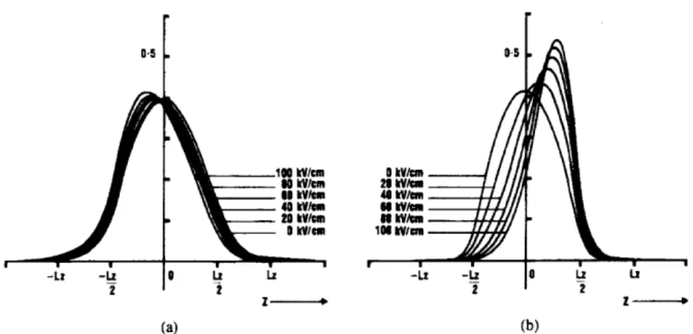
The effects of a perpendicularly applied electric field of strength E upon a quan-tum well energy band structure are shown in Figure 2-6. In addition to the band bending, both the electron and hole wave functions are separated and pulled to op-posite walls in the well, as displayed in Figure 2-7 [2]. The heavy holes exhibit a stronger reaction than electrons to an applied electric field due to their heavier mass and lower energy barrier [14]. Though the electron-hole Coulombic attraction is main-tained, their binding energy is reduced by the wave function separation. A change in the intersubband separation (effectively, the energy of the bandgap of the quan-tum well, Sg), however, counters the binding energy reduction. The shifting of the wave functions creates a smaller overlap between them, which in turn reduces the absorption in relation to the band edge. At this point, the Stark effect, enhanced by the presence of bound excitons, dominates over the slight changes in intersubband energy, resulting in a small change in the quantum well bandgap energy, £g,. In the quantum-confined Stark effect, named after the specific case for which the Stark
Figure 2-6: Energy band diagram of a quantum well in the presence of an applied electric field of strength E. The field induces band bending as well as shifting of the electron and hole wave functions.
effect occurs in quantum wells, an increase in electric field strength results in 1) a decrease of gw,, 2) a shifting of the absorption spectrum to longer wavelengths (lower
energy) as shown in Figure 2-8 [2] and 3) an induced change in the refractive index, n, close to the absorption edge. To produce a sufficiently large An, as required for phase modulation, the absorption spectrum should be moved further into the band edge where absorption is reduced.
Changes in n, as a result of Aao, are determined through the Kramer-Kronig relation that was previously discussed in Section 2.5. In Figure 2-9, Thistrup [3] identifies three types of shifts in a, induced by an electric field, and the corresponding change in n that occurs as a result. In the first case, the introduction of an electric field causes a shift in the absorption edge from a shorter (A2) to a longer wavelength
(A3), presented in the top plot of Figure 2-9 (a). The change in the refractive index
corresponding to this specific situation is expressed by
AnI(A) = A l+n (A )(-A2) (2.12) 4T2 r(A- A3)(A + At)
The resulting transformation in An (as shown in the bottom plot of the same figure)
kV/cm kY/cm kV/cm kVlm kY/sm 0 kV/cm 28 k/Wm 48 k/m N k/cm 186 Y/as Z- Z (a)
Figure 2-7: Plot of normalized wave functions in the presence of varying electric fields of a Lz=10.5 nm well, obtained by G. Lengyel et al [2]. The electron wave function in (a) and the heavy hole wave function in (b) can be seen shifting with increasing electric field strength.
is a positive one. In the second case, the change in refractive index is described by
4 (A + A2)(A + A1)
n
~(( (A-- -= 2) (2) -n (2.13)42
-
+
)
The reduction in a is induced by an electric field within the wavelength range of A1 to the longer wavelength A2. The subsequent change in n [presented in the bottom
plot of Figure 2-9 (b)] is negative according to Equation 2.13.
The final case, presented in Figure 2-9 (c), of absorption change is a combination of the first two cases. The absorption edge undergoes both a shift from A2 to A3 as
well as a reduction in a in the wavelength range between A1 and A2. The combined
effects of the the two scenarios yields an expression for the change in the index of refraction given by
Anmi(A) = An(A) + An 1(A) (2.14)
where Ani(A) and Anii(A) represent the changes in the index of refraction as a result of a shift in the absorption spectrum in case I and reduced absorption in case II respectively.
The quantum well width of quantum-confined Stark effect-based modulators must
" 25000 2000 10000 5000 0 Energy (v) 1.48 1.47 1.46 1.45 1.44 1.43 830 840 850 860 170 Wavelength (nm)
Figure 2-8: Absorption spectra measurements of a Lz=10.5 nm well, obtained by G. Lengyel et al [2] as a function of applied electric field.
be chosen wisely. A smaller width, L, will yield a larger a which is beneficial for an amplitude modulator. However, if the well is too thin, both the electron and hole wave functions will spread beyond the low index layer, reducing their overlap and consequently reducing a as well. On the other hand, a wide quantum well would improve the Stark shifting, but would weaken the electron-hole interaction and exciton binding energy [15]. With these considerations in mind, Tobin and Bruno [16] adopted two approaches in designing a modulator operating at 810nm. The first technique involves embedding low Al content AlGal_-As layers between Al0.3Ga0.7As layers,
and preserving the Stark shift by designing wide quantum wells. An appropriate choice for Al content x in the quantum layers will move the photon transition energy to the desired 810nm. The transition energy, Sph, is given by
Sph = Se + 6h + Sgw - $ex (2.15)
The second method taken to design such a modulator uses several GaAs quantum wells separated by thin Alo0.Ga 0.7As layers in order to create one effective quantum
well that is sufficiently large for Stark shifting. The coupling between GaAs quantum
---TYPE I Sr--- al 1.2 1.0 0.6 O.4 n2 0.0 0.16 I 0.12 I 0.06 I 0.04 ii 0.00 -0.16 Woveength WWv~ngth 0.16 I 0.12 I 0.08 I 0.041 0.00 -00 -0.04 -0.12 -0.16 1 Wove . ,gth2 Wolmenth
Figure 2-9: Comparison of the absorption coefficient by Thirstup [3] (top images) during material excitation (dashed line) and no excitation (solid), and corresponding effects on the index of refraction (bottom images) in three different cases. In (a), the absorption edge is shifted from a shorter A2 to a longer wavelength A3. In (b),
a change in a is induced by an electric field specifically within the wavelength range of A1 to the longer wavelength A2. In (c), absorption change is a combination of the first two.
wells can then be modified to alter the photon transition energy in the modulator heterostructure until 810nm is achieved.
2.2.4
Electro-optic Effect
Within a medium, the constitutive relation
S= EO + V (2.16)
describes the dependence of the electric displacement vector, V, on the electric field vector, 2, and polarization vector, 7. The permittivity of free space, co is related
to the dielectric tensor through
Ej =
E0(1+ e)
_ _ (2.17) ( ( € € (where X is the susceptibility tensor which is dependent upon crystal structure. When
no electric field is applied, co is linked to the n of an anisotropic crystal by
n = I(2.18)
for permeability M and free-space permeability o0. In non-magnetic materials as in the case of most compounds, y = Mo.
In an isotropic medium, 3 and P are parallel and the refractive index value is the same in all axes. In an anisotropic medium, an incoming beam breaks down into two components - the ordinary and extraordinary waves - by double refraction. The two wave types travel with differing speeds on different paths with distinct indices of refraction. Consequently,
i
andI-
are not parallel, and the refractive index is not equal in all axes. An example of double refraction is depicted in Figure 2-10 for the case of a uniaxial material, where n, = nz while n along the y axis differs. TheIncident z M . . .
x
:traordinary urdcnary
Figure 2-10: Split of an incident beam into ordinary and extraordinary rays in a uniaxial crystal.
ordinary component of the incoming beam is polarized in the y direction and the extraordinary wave is polarized in the xz plane. In a uniaxial crystal, two of the axes have identical indices of refraction called the ordinary index, no, and obey Snell's law
for the angle of refraction of the ordinary wave (0o), the angle of the incoming beam (0j) and the refractive index (ni) of the medium through which the incoming beam
travels. The index of refraction of the third axis is the extraordinary index, ne, calculated by
1 cos2 9e sin2 e (2.20)
- = +(2.20)
n2 n2 n2
with 9O representing the angle of refraction of the extraordinary wave. The general
case of a biaxial crystal (for which all axes have different indices) is expressed as an index ellipsoid of the form
x2 y2 2
-n + n2 = 1 (2.21)
describing the birefringence within such a medium.
As in the Franz-Keldysh effect, the introduction of an electric field modifies a material's n. However, since there are no carriers, and therefore, no absorption that was present in the Franz-Keldysh effect, both phase and amplitude modulation rely upon an induced An. This type of modulation is known as transverse electro-optic modulation, as the applied electric field is perpendicular to an incoming light beam, and is accomplished through the use of the electro-optic effect.
With the application of an electric field of strength E, the index ellipsoid takes on the altered form of
-+A 1)X 2 + n-I+A 1)y2+(n- +A 1 )z2 +A-
1.2yz+A-
2xz+A-1 2xy= 1
S
+
n2 n2 n 2 n2 n)2 2yz+ 2xz+ n 2xy =y y z z yz xz xy
(2.22)
where ni is the induced index of refraction in a distinct axis or plane i. With no applied electric field, all A' = 0 and the equation is reduced to Equation 2.21. The change in n with respect to the applied electric field is defined by the Kerr effect as follows:
1
A = r lE + sqE2 (2.23)
ni
When r1, the linear electro-optic coefficient, is much larger than sq, the quadratic electro-optic coefficient, the first term dominates and the relationship between the
applied electric field along each axis and material impermittivity becomes
1 6
A 2 = rijEj i j=1
(2.24)
where rij is the electro-optic tensor matrix. This is the linear case of the electro-optic effect known as the Pockels effect, and may also be written in matrix-form:
A' A'n2 A' A ' n2yz A-L nz xy rIll T'21 T31 T41 r61 r61 r22 73 2 r42 r52 r62 71 3 T23 733 743 r53 r63
For GaAs, an isotropic cubic crystal with inversion symmetry, rij is reduced to
four-fold symmetry of group 43 that lacks
0 0 0 0 r5 2 0 0 0 0 0 0 r63
where r41 = r52 = r63 for isotropic materials. In a uniaxial material, T4 1 = r63 but the
y axis coefficient remains as r52. For a y-directed electric field in a uniaxial system,
An is
1
A 2 =r 52E
n2XzZ (2.25)
and Equation 2.22 reduces to
X2 y2 Z2
2 2 2 + 2r52Eyxz = 1
no n n
A comparison between Equation 2.21 and Equation 2.26 reveals a mixed term, 2r52Eyxz. The applied electric field Ey distorts and rotates the ellipsoid from a circle
z @y
Figure 2-11: Index ellipsoid under an applied electric field in the y-direction.
in the xz plane to the ellipsoid rotated by an angle 0 off the xz plane (shown in Figure
2-11). When n. = nz and A-L = A- = 0, then 0 = 450 [17]. A new coordinate
system is developed using new principle axes x', y' and z' defined by
x = x cos - z sin - = 4 4 z = x' sin- + ' cos 4 4 X= + z y = y' (2.27) (2.28) (2.29) Using Equations 2.27 and 2.28,
x'2 z12
XZ =-
-2 2
and the mixed term due to the electric field is transformed into the expression
2r.2Eyxz = r52Ey(xZ2 - z'2)
(2.30)
The former x and z axis terms in Equation 2.21 are also transformed into
X12 Z12
n2 no (2.32)
The combination of Equations 2.26, 2.31 and 2.32 yields a new expression for the index ellipsoid associated with the new principal axes:
o y
1
+ (o - r52E,)z'2 = 1
Equation 2.33 has the same form seen previously in Equation 2.22, so it may be inferred that
1
A n2 = r52E (2.34)
and therefore n' and n' may be written as
n = no + AnX, (2.35)
and
n = no - AnZ (2.36)
By linearization, the following expression for the field-induced change in the index of refraction is derived:
1 1 1
An = -- n A- = n3 r52Ey
2 n2 2 (2.37)
Finally, Equation 2.37 is applied to the former expressions for n' and n' to obtain
Q
(2.38) n. = no - -n T52Ez,
1r52E
n' = no + -n3r52E (2.39)
Now that the electric field effect on the refractive indices of different axes is known, (2.33)
and
the electric field and voltage required to achieve a desired phase modulation can also be calculated. Figure 2-12 shows a basic waveguide with top and bottom electrodes to which a voltage V is applied, creating an electric field, E,, oriented along the y axis. When an electric field is applied to a GaAs-based modulator along a distinct
y
Incoming Beam
I
Figure 2-12: Basic waveguide modulator operating on the electro-optic effect. An applied voltage V creates an electric field, Ey, that induces a An in the x and z axes.
axis, the other two axes will show a change in refraction. In this case, the applied electric field Ey results in induced n' and ni.
An incoming beam directed along the z axis has a TE component along the x
axis and a TM component along the y axis. Hence, the TE mode will be affected by the modified n'x, while the TM mode lying on the same axis as the electric field, will not feel the effects of a An. As a result, only the TE mode of the beam will undergo modulation, reducing the device efficiency [18].
In general, the expression for the total phase shift of a beam traveling along the
z axis, associated with a normal electric field in the y axis, is
A = koLAn = 27 r5E (2.40)
A 2
where ko is a wavevector equal to 2, L is the modulator length and A is the wavelength of operation. The voltage applied yielding Ey is given by
V = E, - tg (2.41)
the phase shift achieved by a certain applied voltage V is obtained through
r Ln3r52V
A = L (2.42)
A t9
Consequently, a phase shift of ¢ = ( for example, requires a voltage of
V_ 2 A t (2.43)
2 Ln3r5 2 and a phase shift of = / would require a voltage of
V, =A tg (2.44)
Ln3r5 2
The TE and TM components of an incoming optical beam travel along the x and z axes respectively. If nx Z: nz in the modulator structure, the TE and TM components will acquire different phase velocities due to the differing indices of refraction along each axis of polarization, a phenomenon known as birefringence. Modulators have a natural birefringence by virtue of their structural design computed by
nbirefringence = rTE - nTM (2.45)
where nTE and nTM are the TE and TM mode indices respectively. In bulk
modula-tors of isotropic materials such as GaAs, ne = no and there is no natural birefringence. However, in heterostructures and uniaxial crystals where ne 7 no, nbirefringence does exist and often dominates over the induced index change. Though this effect is useful in polarization modulation, nbirefringence should be minimized for both phase and am-plitude modulation so that TE and TM modes are similarly modulated. Minimization of birefringence is accomplished by designing a structure with a near-uniform material arrangement, so that the mode is surrounded by the same layer configuration along its extraordinary and ordinary axes.
Efficient modulator design is associated with lower operating voltages and min-imal device dimensions. Consideration of the wafer crystal orientation is critical in
determining the placement of devices on the sample. Correct alignment of devices with the x' and z' axes will allow maximal modulation of the TE component of an entering optical beam. Device alignment with crystal orientation also controls the quality of the cleave. Consequently, devices aligned to the x' and z' axes will result in cleaner and easier cleaving of the wafer.
2.3
Modulation Structures
In addition to several modulation methods, there are also structures that may be em-ployed to produce phase changes. Fabry-Perot interferometers and coupled-waveguide devices both offer techniques for phase modulation, that in-turn can result in inten-sity modulation. This work focuses on the use of Mach-Zehnder interferometers that translate phase modulation to changes in signal amplitude by light wave interference.
2.3.1
Mach-Zehnder Interferometers (MZIs)
In a Mach-Zehnder interferometer, a light beam entering from a passive waveguide is split into two components which then travel along two optical paths and recombine at the output as depicted in Figure 2-13. If the path lengths are identical, the beams will be in phase at the output and interfere constructively. However, when the path lengths vary, a phase difference between the two beams will be introduced and affect the total power at the output. The path length can be changed by applying a voltage across
Beam Recombination
Figure 2-13: Mach-Zehnder interferometer that uses the interference of split beam components to produce a change in total beam intensity. The beam splitter in this particular case is a Y-splitter.
one or both of the arms (as shown in Figure 2-14), thereby creating active waveguide regions. The electric field causes a relative phase change between the two arms that results in intensity modulation at the output. If, for instance, a voltage is applied to one arm corresponding to AO = 7r, the relative phase difference between the two
beams will also be 7r. In this case, a single-mode output waveguide that supports only first-order modes will exhibit a resulting intensity of zero for that mode. All light corresponding to unsupported modes will dissipate by radiating into the substrate [19, 20]. The interferometer may also be used with a push-pull drive by powering one
Figure 2-14: Mach-Zehnder interferometer with electrodes over both arms. The path length will vary with applied voltage and affect the total output power.
arm with positive voltage and the other with negative voltage. This technique has the added benefits of doubling device efficiency and reducing the required active arm length by two [21].
Chapter 3
Design
The ultra broadband modulators developed in this work operate according to the electro-optic effect described in Section 2.2.4. The electro-optic effect has been chosen due to the large optical bandwidth requirement of the structure (approximately 650nm
- 950nm) for which an electroabsorption-based effect would not have been sufficient. Furthermore, the effect relies upon changes in the index of refraction, n, as opposed to the absorption, a, which involves carriers. Therefore, no loss due to free carrier absorption is expected (carriers present in the contact layers are optically negligible). The design of such modulators combines multiple aspects, from considerations of mode confinement and TE/TM mode properties to material choices and device voltage requirements. Calculations of mode propagation and behavior are essential in order to determine specific waveguide lengths and radius of curvature as well as potential losses involved, and to proceed to the next step of designing a mask, and ultimately, fabricating the device.
3.1
Optical Simulation
Commercial simulation software was used to model the mode properties and to de-termine the mode confinement capability of a specific layered structure. Optical simulations allow the user to vary materials and thicknesses and resolve their effects on mode behavior. In addition, mode propagation through waveguide bends was
simulated for different bend radii. The information provided by simulation software is critical in device and material design, and requires a discussion of the calculation methods employed in the programs.
3.1.1
3-D Mode Solver
The computation of mode properties is an imperative first step in the process of mod-ulator design. Simulations provide information regarding a heterostructure's effective index of refraction and waveguide capabilities in supporting first-order modes only. The Optiwave software programs, OptiBPM 5.2 and OptiBPM 6.0, were employed in modeling a modulator layer structure, Y-splitters and multimode interferometers (MMIs). The simulations are based upon the beam propagation method (BPM) with alternating direction implicit (ADI) method that solve the semivectorial Helmholtz equation. The software provides mode eigenfunctions and propagation constants, and outputs numerical modal effective indices and fields as well as their graphical repre-sentations. This section provides an overview of the methods used in OptiBPM 6.0 to calculate modal indices. The reader is referred to references [22, 23] for a more detailed explanation.
A scalar electric field is separated into its space and time components through E(x, y, z, t) = ¢(x, y, z)e- jwt. The Helmholtz equation for steady state (and inclusive only of the spatial component ¢ of the electric field) is given by
1
92 + 0Z2 + k(x, y,z)2 = 0 (3.1)
where the wavenumber k(x, y, z) = kon(x, y, z) = [n(x, y, z)], related the refractive index distribution n(x, y, z) with applied electric field. Phase variation caused by propagation along the z-axis accounts for the fast variation in ¢. As a result, the field may be depicted as a slow-varying envelope field u(x, y, z) by separating the field from
phase variation through the approximation
with the reference wavenumber k representing average variation in the phase of the field
4.
Similar to k, k is related to the reference refractive index n through k = k0-.The Helmholtz equation in combination with Equation 3.2 for a slow-varying field u yields the form
&2u 02u 02u -Ou
)2
x---+ y2 2 + aZ2 + 2jk (9 + (k2 )u = 0 (3.3)
If field variation along the z axis is assumed to be sufficiently slow, so that 2 is negligible in comparison to the first partial term 2k , Equation 3.3 is transformed into the standard beam propagation equation:
au
j
(0
22U
2 _2)- = 2 -- + + (k2 - 2)u)
(3.4)
az
2k (aX2
ay2
In solving this basic type of three-dimensional beam propagation problem, transpar-ent boundary conditions are assumed with no reflections (they would impede steady-state calculations). Transparent boundary conditions provide a better option than the method of inserting artificial absorption regions, where the region's varying a, thickness and shape are all problem-specific and not useful for general case calcula-tions. Furthermore, if the gradient in a over the region is too large, reflections may occur. For more details on these approaches, please consult [24].
Equation 3.4 may also be represented in matrix form as
9 PX P Xy (3.5)
for differential operators Pij, where Px, and Py, explain cross-coupling effects between the normal fields. The Pij matrix is written as a function of its x- and y-dependent components as follows:
PXX P,
A + AA
B
)PxI Py C Ayy + Ayy
constants Axx and AY represent the TE and TM mode propagations and field shapes respectively, while Ax, and Ayx are related to geometry-induced polarization coupling.
The semi-vectorial form of the BPM equation seen earlier assumes that the diag-onal coupled terms, B and C, are negligible. This assumption leads to the following set of equations:
Bu
S=
Axxu + AxYuy(3.7)
Ou
= A.yuy + AyXUX (3.8)
The Aij terms representing propagation constants defined in conjunction with the ux and uY slowly varying field terms provide the full expressions for the semi-vectorial equations: Axxux = (n2x) + (k2 2)u~ (3.9) 2k ax n 2
ay
2 AxU = n2 axay (3.10) AyYUY = j+ay
(n
+ (k2- k2) U (3.11) AyXUXn a± (2x) (3.12) 2 k ay n2 (k.ax )The technique used to solve the semi-vectorial equations is explained for an x-polarized mode propagating in the z direction with the understanding that the same method may be applied to a y-polarized mode. In order to solve the expression for semi-vectorial beam propagation, the form undergoes discretization by the Implicit Crank-Nicholson scheme. The discretization rewrites the problem as a finite difference equa-tion in a mesh with grid points equally spaced along the x axis and for planes equally spaced along the z-axis. At a given grid point i, the slow-varying electric fields are evaluated at a longitudinal midplane situated between plane n for which the field is known, and the following plane n + 1 in which the field is not known. This method has proven unconditionally stable for all Az and is accurate to the second order in
![Figure 2-1: Optical pulse generation (top) by envelope superposition over a carrier wave in the time domain, and resultant frequency comb generation (bottom) in the frequency domain [1]](https://thumb-eu.123doks.com/thumbv2/123doknet/14744687.577784/23.918.235.685.149.574/optical-generation-envelope-superposition-resultant-frequency-generation-frequency.webp)

![Figure 2-9: Comparison of the absorption coefficient by Thirstup [3] (top images) during material excitation (dashed line) and no excitation (solid), and corresponding effects on the index of refraction (bottom images) in three](https://thumb-eu.123doks.com/thumbv2/123doknet/14744687.577784/33.918.194.739.127.421/comparison-absorption-coefficient-thirstup-excitation-excitation-corresponding-refraction.webp)
![Figure 3-1 [4] displays the various bandgap energies, lattice constants and emission wavelengths of popular and heavily-used III-V binary materials such as GaAs and InP](https://thumb-eu.123doks.com/thumbv2/123doknet/14744687.577784/52.918.284.653.426.692/figure-displays-various-energies-constants-emission-wavelengths-materials.webp)


