Diffractive Optics for Maskless Lithography and
Imaging
by
Rajesh Menon
B. E. Electrical Engineering, Nanyang Technological University (1998)
S. M. Electrical Engineering, Massachusetts Institute of Technology (2000)
Submitted to the Department of Electrical Engineering and Computer
Science
in partial fulfillment of the requirements for the degree of
Doctor of Philosophy
at the
MASSACHUSETTS INSTITUTE OF TECHNOLOGY
May 2003
@
Massachusetts Institute of Technology 2003. All rights reserved.
Author ...
...
Department of Electrical Engineering and Computer Science
May 21, 2003
C ertified by ...
/
Henry I. Smith
KeithleyProfessor of Electrical Engineering
Thesis Supervisor
Accepted by ...
Arthur C. Smith
Chairman, Department Committee on Graduate Students
MASSACHUSETTS INSTMUlTE OF TECHNOLOGY
Diffractive Optics for Maskless Lithography and Imaging
by
Rajesh Menon
Submitted to the Department of Electrical Engineering and Computer Science on May 21, 2003, in partial fulfillment of the
requirements for the degree of Doctor of Philosophy
Abstract
Semiconductor industry has primarily been driven by the capability of lithography to pattern smaller and smaller features. However due to increasing mask costs and complexity, and increasing tool costs, the state-of-the-art technology in lithography is accessible only to a select few.
Zone-plate array lithography (ZPAL) is a novel method of maskless lithography that aims to alleviate some of these issues while offering a solution that can be extended to the limits of nanolithography. In ZPAL, an array of diffractive lenses is used to form an array of spots on the substrate. Each spot is modulated independently by means of spatial-light modulators. This essentially creates a "parallel laserwriter". In addition, this lithography system can be converted into a parallel-confocal microscope, which enables fast, high-resolution imaging.
This thesis addresses the performance of diffractive lenses, particularly high-numerical aperture zone plates for lithography and imaging using a combination of experimental and theoretical studies. A novel proximity-effect correction algorithm that was implemented effectively in a ZPAL system is also described. Variations to another diffractive lens known as the photon sieve are proposed. The first ever lithography results performed using these new elements are presented in this thesis.
Thesis Supervisor: Henry I. Smith
Acknowledgments
Firstly, I would like to thank Professor Henry Smith for giving me the opportunity to work on this project. To understand with academic rigor is one of the important lessons I have learnt from him. I thank him for giving me the freedom to direct the research based on my intellectual curiosity.
Dr. Dario Gil has been a wonderful friend throughout my stay at MIT. His perseverance, technical prowess, and intellectual conscientiousness in science as well in social issues will always be an inspiration for me. I thank Dr. David Carter for being a patient mentor, and succeeding in transforming me from a theorist into an experimentalist! Dario and David have been instrumental in the success of this research.
I have great respect for Professor George Barbastathis, who has been a champion of this work. He has been a constant source of encouragement and suggestions throughout the course of this research. I am also extremely grateful for his friendship.
Several past and present members of the NanoStructures laboratory namely Dr. Todd Hastings, Dr. Thomas Murphy, Dr. Farhan Rana, Dr. Juan Ferrera, Feng Zhang, Michael Walsh, Mark Finlayson, Minghao Qi, Tim Savas, Thomas O'Reilly, Dr. James Goodberlet, Dr. Mitchell Meinhold, Tymon Barwicz, Amil Patel, Dr. Mark Schattenburg, and Dr. Paul Konkola have helped in shaping this research project.
I am very grateful to James Daley for showing me the ropes for almost everything inside the clean-room. His patience, good-nature, and hard-work has always impressed me. Much
thanks is owed to Jimmy Carter for helping me with the scanning-electron microscope. For a long time, Mark Mondol was my only connection to India at the NanoStructures laboratory. I thank him for this and all his help with electron-beam lithography.
Professor Dennis Prather and his students at the University of Delaware were extremely helpful with several aspects of the simulation tools used in this work.
I thank Cindy Lewis for help with all administrative work during my stay at MIT. Euclid Moon has been my officemate, and friend since I first joined the NanoStructures laboratory. I greatly apreciate our discussions on science and philosophy. I will always treasure the adventures we have shared, especially the time spent admiring music and nature
at the Fusion Festival!
Paul Herz was my first and truest friend at MIT. I am forever grateful to him for his support through all the changes in my life.
I would like to express appreciation to my psy-trance family including Sasha, Selim and Yannis, I will miss our "Krysalis" gatherings.
Thanks also goes to Juliet Gopinath and Joyce Wu for being my steadfast friends from the very beginning.
I would like to extend my gratitude to the Hewetts especially Mother (Sheila), Laurie, Rebekah, and Patrick for welcoming me with open arms into their family. I can hardly wait for our future family reunions!
My family has been instrumental in my success. My only sister, Rakhee and her husband, Vijay have supported me through everything. I owe all my success to my wonderful parents, who have been patient with me through my long absences, and have been supportive of all my decisions. I would like to honor my grandparents by dedicating this thesis to them.
Finally, I would like to thank my wife, Marianne. She is my best friend and my soul-mate. She always brings hope into the darkest moments. I thank her for being so kind and understanding with me. I am forever grateful to her for bringing such joy and hope into my life.
Contents
1 Introduction to Maskless Lithography 15
1.1 Mask-based lithography . . . . 15
1.2 Maskless Lithography . . . . 16
1.3 The Case for Maskless Lithography . . . . 17
1.4 Forms of Maskless Lithography . . . . 22
2 Introduction to Zone-Plate-Array Lithography 27 2.1 System Description . . . . 27 2.1.1 Radiation Source . . . . 29 2.1.2 Micromechanical Multiplexers . . . . 30 2.1.3 Zone-Plate Array . . . . 39 2.1.4 Scanning Stage . . . . 39 2.2 Advantages of ZPAL . . . . 40
3 Zone Plates for Lithography 43 3.1 Zone-plate as a Diffractive Lens . . . . 43
3.1.1 Design of a Zone Plate . . . . 44
3.1.2 Diffraction Efficiency . . . . 46
3.2 Simulation of Zone Plates . . . . 49
3.2.1 Fresnel-Kirchoff Diffraction Theory . . . . 49
3.2.2 Vector Diffraction Theory . . . . 53
3.3 High-Numerical-Aperture Effects in Zone Plates . . . . 60
3.3.2 Shadow Effect . . . .
3.3.3 Inter-zone coupling . . . .
3.4 Fabrication of Zone-Plate Arrays . . . . .
4 Lithographic Performance of Zone Plates
4.1 Lithographic Figures-of-Merit . . . .
4.1.1 Contrast and Resolution . . . .
4.1.2 Depth of Focus . . . .
4.1.3 Throughput . . . .
4.2 Lithographic Simulation Process . . . .
4.3 Simulation Results . . . .
4.3.1 Image Contrast . . . .
4.3.2 Effect of Fabrication Errors . . . .
4.3.3 System-level Tolerances . . . .
4.4 Lithographic Performance of Zone Plates: Experiments . . .
4.4.1 Experimental Process . . . .
4.4.2 Experimental determination of Point-Spread Function
4.4.3 Experimental Determination of Exposure Latitude.
4.4.4 Experimental Determination of Image Contrast . .
4.5 Stitching in ZPAL . . . . 4.6 Quality of patterning in ZPAL . . . .
(PSF)
5 Proximity Effects and their Correction
5.1 Origin of Proximity Effects in ZPAL . . . .
5.2 Proximity Effect Correction (PEC) . . . .
5.3 How does PEC in ZPAL compare to other lithography techniques ?....
5.3.1 Electron-Beam Lithography . . . .
5.3.2 Optical-Projection Lithography . . . .
6 Zone-Plate-Array Microscopy
6.1 Introduction to Zone-Plate-Array Microscopy . . . .
67 69 71 75 75 76 85 89 96 101 101 106 113 118 118 120 124 131 133 137 145 145 148 166 166 168 171 171
. . . .
. . . .
. . . .
6.2 6.3 6.4 6.5 Theory . . . . Knife-Edge Scans . . . . Imaging with ZPAM . . . . .
Applications of ZPAM .... 173 176 182 186 193 193 7 Photon Sieve 7.1 Introduction
7.2 Photon Sieve Design . . . 194
7.2.1 Phase-Photon Sieves . . . . 200
7.2.2 Size of the Focussed Spot in a Photon Sieve . . . . 201
7.2.3 Depth of Focus . . . 201
7.2.4 Apodization . . . . 202
7.2.5 Efficiency of the Photon Sieve . . . . 203
7.3 Fabrication of Photon Sieves . . . . 204
7.3.1 Amplitude-Photon Sieve . . . . 205
7.3.2 Alternating-Phase Pinhole Sieve . . . . 206
7.3.3 Phase-photon sieve . . . . 206 7.4 Lithography using Photon Sieve . . . .
A Scalar Diffraction Theory
A.1 Fresnel-Kirchhoff Diffraction Theory . . . . A.1.1 Validation of numerical Code : Square Aperture . . . . . A.1.2 Validation of numerical code: Sinusoidal Grating . . . . A.1.3 Validation of numerical code: Zone Plate . . . . A.2 Fresnel Approximation of Fresnel-Kirchhoff Diffraction Equation
207 211 211 213 215 216 217
B Derivation of Diffraction Efficiency for Zone Plate with general Phase Shift221
C Relation of knife-edge data to Radon Transform 225
List of Figures
1-1 Simplified schematic of an optical stepper. . . . . 1-2 Simplified schematic of a scanning-electron-beam-lithography tool. 1-3 Escalating cost of optical lithography tools .. . . . . 1-4 Trend towards subwavelength lithography. . . . . 1-5 Escalating cost of masks. . . . . 1-6 Schematic of a system using variable masks. . . . . 1-7 Schematic of the Micronic Systems maskless lithography tool. . . 1-8 Scanning Spot Maskless Lithography. . . . .
2-1 2-2 2-3 2-4 2-5 2-6 2-7 2-8 2-9 2-10 2-11 2-12 2-13
Schematic of a Zone-Plate-Array Lithography system. . . . . Schematic of the components of a ZPAL system. . . . . Photograph of the diode laser. . . . . Texas Instruments Digital Micromirror Array. . . . . Patterns written in parallel using the TI DMDTM.. . . . .
Silicon Light Machines Grating Light Valve. . . . . GLVTM in ZPAL. . . . .
Experimental verification of the performance of the GLVTM. . . Boston Micromachines SLM. . . . . Microshutter arrays being developed at NASA. . . . . Microshutter actuation methods. . . . . Microshutter array device invented at MIT Lincoln Laboratories Scanning stage from Physik Instrumente . . . .
. 16 . 17 . 18 . 19 . 20 . 23 . 24 . 25 . . . . 28 . . . . 29 . . . . 30 . . . . 31 . . . . 32 . . . . 33 . . . . 34 . . . . 35 . . . . 36 . . . . 37 . . . . 38 . . . . 39 . . . . 40
3-1 Schematic of a zone plate. . . . . 44
3-2 Numerical Aperture of a zone plate. . . . . 45
3-3 Diffraction orders of a zone plate. . . . . 49
3-4 Huygens' Principle. . . . . 50
3-5 Fresnel-Kirchoff formulation for diffraction from a general aperture. . . . . . 51
3-6 Cartesian grid for FDTD. . . . . 56
3-7 Spacetime diagram of 1-D wave solution using FDTD . . . . . 57
3-8 Spatial FDTD domain for simulating one zone plate. . . . . 59
3-9 Zone width as a function of zone number . . . . . 61
3-10 Form birefringence in a high-NA zone plate. . . . . 62
3-11 Circular Polarized Light. . . . . 63
3-12 Rotation of the coordinate system. . . . . 64
3-13 Focussed spot with linear and circular polarized light. . . . . 65
3-14 Spot size as a function of NA. . . . . 66
3-15 Shadow effect in high-NA zone plates. . . . . 67
3-16 Focussing efficiency as a function of NA. . . . . 68
3-17 Inter-zone coupling. . . . . 70
3-18 Fabrication of zone plates. . . . . 72
4-1 Definition of image contrast. . . . . 76
4-2 Relationship between image contrast and resolution. . . . . 78
4-3 Typical contrast curve of a positive photoresist. . . . . 79
4-4 Minimum resolvable-image contrast versus resist contrast. . . . . 80
4-5 Contribution of resist advancements to high-resolution lithography. . . . . . 81
4-6 Experimental determination of resist contrast. . . . . 82
4-7 Effect of photoresist on sidewall angle. . . . . 83
4-8 Resist sidewall angle for gratings of different densities. . . . . 83
4-9 Change of exposure dose leads to change of linewidth. . . . . 84
4-10 Effect of defocus on the focussed spot. . . . . 86
4-12 4-13 4-14 4-15 4-16 4-17 4-18 4-19 4-20 4-21 4-22 4-23 4-24 4-25 4-26 4-27 4-28 4-29 4-30
Rotation of zone-plate array for efficient scanning. . . . . Scan Strategy with rotated zone-plate array. . . . . Tiling the hexagons to cover the entire substrate. . . . . Throughput as a function of NA. . . . . PSF of a NA=0.7 zone plate. . . . . Process for simulating patterns in ZPAL. . . . . Effect of multiplexer ON-OFF contrast on image contrast. . . . Effect of boundary conditions on image contrast .. . . . . Effect of PSF-truncation radius on image contrast. . . . . Effect of the s-factor on exposed patterns. . . . . Effect of the s-factor on image contrast. . . . .
Effect of NA on the PSF. . . . .
Effect of NA on image contrast for different grating periods. . . Effect of defocus on image contrast for different grating periods. Cross-section of a phase zone plate. . . . . Schematic of phase-shift error (etching error). . . . . Effect of phase-etch error on the first-order diffraction efficiency. Image contrast versus etching error for lines/space patterns. . . Schematic illustrating duty-cycle errors .. . . . .
4-31 Image contrast versus error in duty cycle for dense gratings of various linewidths and different densities. . . . . 4-32 Schematic illustrating possible zone placement errors (radial period errors). 4-33 Image contrast versus zone-radii errors for dense gratings at various linewidths
and densities. . . . . 4-34 Maximum source bandwidth as a function of zone-plate numerical aperture
(N A ). . . . .
4-35 With zone plates, as is the case with lenses, the focused spot can be swiveled by illuminating the zone plates obliquely. . . . . 4-36 Image contrast as a function of the angle of illumination for dense gratings of
various linew idths. . . . .
. . . . . 90 91 92 . . . . . 93 . . . . . 96 . . . . . 97 . . . . . 98 99 . . . . . 100 . . . . . 102 . . . . . 103 . . . . . 104 . . . . . 105 . . . . . 105 . . . . . 106 . . . . . 107 . . . . . 108 . . . . . 109 . . . . . 109 110 111 112 115 116 117
4-37 4-38 4-39 4-40 4-41 4-42 4-43 4-44 4-45 4-46 4-47 4-48 4-49 4-50 4-51 4-52 4-53 4-54 4-55 4-56 4-57
Resist and ARC stack used in the experiments. . . . .
Experimental process for determining the PSF using lithography. . . . . .
Exposure-dose samples for the experimental determination of PSF. . . . . Point-spread functions of NA=0.85, 0.8 and 0.7 zone plates. . . . . Focussing efficiency as a function of NA. . . . . Experiment for determination the exposure latitude. . . . . Experimental determination of exposure latitude for a NA=0.9 zone plate. Experimental determination of exposure latitude for a NA=0.85 zone plate. Experimental determination of exposure latitude for a NA=0.8 zone plate.
Smallest period gratings with s=1. . . . . 130
Smallest period gratings with s=2. . . . . 130
Determining contrast from grating exposures. . . . . 131
Image contrast as a function of grating period. . . . . 133
Schematic illustrating stitching errors. . . . . 134
Angular misalignment of ZPA and stage axes. . . . . 135
Measuring the angular misalignment between the ZPA and the stage axes. 135 Experimental results showing stitching across unit-cell boundaries. . . . . 136
Patterns with curves written with ZPAL. . . . . 139
Miscallaneous patterns written with ZPAL. . . . . 140
Portrait patterned using ZPAL. . . . . 142
Full-field patterning with ZPAL. . . . . 143
Background in the PSF. . . . . Schematic illustrating proximity effects. . . . . Demonstration of proximity effects. . . . . Schematic illustrating the use of dose modulation for PEC. . . . . 146
. . . . 147
. . . . 148
. . . . 149
5-5 Linewidth control and edge-placement control using dose modulation and
sub-pixel stepping. . . . . 5-6 Proximity-effect correction by dose modulation. . . . . 5-7 Writing technique in ZPAL. . . . .
150 151 152 118 120 121 123 125 126 127 128 129 5-1 5-2 5-3 5-4
5-8 Simulation results of PEC with the LP method. . . . .
5-9 Schematic illustrating the steps involved in the iterative-error- correction method. ... ...
5-10 Simulated pattern corrected using the iterative-error-correction method. . . . 5-11 Effect of space-grid size on PEC. . . . .
5-12 Effect of spacing of exposed spots (s-factor) on PEC. . . . . . 5-13 Effect of quantization of dose on PEC. . . . . 5-14 Mean error as a function of the number of iterations. . . . . . 5-15 Experimental results of PEC using the iterative algorithm. . . 5-16 Magnified images of the experimental results of iterative PEC. 5-17 Focussed spot in an electron-beam lithography system... 5-18 Examples of optical-proximity correction. . . . .
Schematic of confocal microscopy. . . . . Schematic of zone-plate-array microscopy. . . . . Schematic of an ideal scanning-confocal microscope. . . . Lateral resolution of a ZPAM system. . . . . Axial resolution of a ZPAM system. . . . . Knife-edge scan results. . . . . Reconstructed PSF of NA=0.7 zone plate at A = 400 nm. Cross-section through the reconstructed PSF. . . . . Schematic of resolution-test sample. . . . . ZPAM images of resolution-test sample .. . . . . Stitched images from adjacent zone plates to increase the High-resolution ZPAM images. . . . . Satellite zone plates for gapping .. . . . . Schematic of parallel-optical tweezers. . . . . Schematic of a parllalel spectroscope. . . . .
. . . . 172 . . . . 173 . . . . 173 . . . . 175 . . . . 176 . . . 180 . . . . 18 1 . . . . 18 1 . . . . 182 . . . . 183 field-of-view. . . . 184 . . . . 185 . . . . 190 . . . . 19 1 . . . . 191
Schematic of a photon sieve. . . . . Field contributions at the focus due to a single pinhole. . . . . 194 196 156 158 159 . . . . 160 . . . . 161 . . . . 162 . . . . 163 . . . . 164 . . . . 165 . . . . 167 . . . . 169 6-1 6-2 6-3 6-4 6-5 6-6 6-7 6-8 6-9 6-10 6-11 6-12 6-13 6-14 6-15 7-1 7-2
7-3 7-4 7-5 7-6 7-7 7-8 7-9 7-10 7-11 7-12 7-13 7-14
A-1 Comparison of scalar and vector diffraction theories. . . . . A-2 Comparison of scalar and vector diffraction theories in log s
Schematic explaining the focal field behavior. . . . . Amplitude photon sieve. . . . . Scanning-electron micrograph of a photon sieve. . . . . Alternating-phase pinhole sieve. . . . . Phase-photon sieve. . . . . Depth-of-focus of a photon sieve. . . . . Percentage of transmissive area in amplitude photon sieves. Fabrication of an amplitude-photon sieve .. . . . . Fabrication of phase-shifted photon sieves. . . . . Patterning of spots with photon sieves. . . . . Patterning of dense lines with photon sieves. . . . . Patterning of dense lines with high-NA photon sieves. . . .
A-3 Scalar Fresnel-Kirchoff diffraction compared to the vector theory for a square
aperture.. ... ... ... . . .. . .. . .. . . .
A-4 Scalar Fresnel-Kirchoff diffraction predicting the Talbot Effect. . . . . A-5 Compare scalar Fresnel-Kirchoff diffraction to vector FDTD. . . . . A-6 Scalar Fresnel approximation compared to the vector theory. . . . . A-7 Scalar Fresnel approximation compared to the vector theory. . . . .
. . . . 197 . . . . 198 . . . 199 . . . 201 . . . 202 . . . 203 . . . 204 . . . 205 . . . 207 . . . 208 . . . . 209 . . . . 210 . . . . 212 -ale. . . . . 212 215 216 216 219 220
Chapter 1
Introduction to Maskless Lithography
The rapid technological growth since the invention of integrated circuits has been driven primarily by lithography. Lithography refers to the technology used to produce patterns on a substrate such as a silicon wafer. These patterns form the building blocks of integrated circuits and subsequently of the electronic revolution of the 20th century.
There are two main flavors of lithography: mask-based and maskless.
1.1
Mask-based lithography
In mask-based lithography, the master-pattern on a mask is imaged onto the substrate. This technology is illustrated using the example of the optical stepper.
The optical stepper is the workhorse of lithography for the semiconductor industry. Fig-ure 1-1 shows the simplified schematic of an optical stepper. The mask consists of a fused silica substrate with the pattern defined by patches of opaque material such as chromium. The mask is manufactured by means of one of the direct-write (maskless) lithography meth-ods. The pattern on the mask is imaged using optics onto the surface of the substrate. The substrate is coated with a layer of photoresist. Photoresists are materials that undergo photochemical reactions when exposed to light. The photoresist is thus able to record the projected image. Further processing then transfers this image into the silicon wafer. One major drawback of this technique is that the pattern to be printed is fixed by the master
pattern on the mask.
light
mask
optics
e"photoresist
*--substrate
Figure 1-1: Simplified schematic of an optical stepper. The mask contains the master pattern
as depicted by the dark and white regions. The pattern on the mask is imaged onto the surface of the substrate using optics. The substrate surface has a layer of photoresist which records the image of the pattern.
1.2
Maskless Lithography
Maskless lithography, as its name implies, needs no mask. An example will help illustrate the concept. Scanning-electron-beam lithography is the most often used maskless lithography technique. Figure 1-2 shows a simplified schematic of a scanning-electron-beam-lithography system. A beam of electrons is focused using magnetic fields into a spot. This focused spot can be deflected by means of magnetic or electric fields to write desired patterns directly on the resist. In this case the resist is sensitive to the electron-beam. The pattern is thus built up from discrete spots. The major difference from the mask-based approach is that in the electron-beam system, the same focused spot can be used to write any arbitrary pattern, just by changing the deflection pattern of the beam.
One common theme in maskless lithography is the fact that the pattern information,
instead of being stored in the form of a physical mask ( which is a very efficient but expensive
electron gun
deflection coils
resist
4-
substrate
Figure 1-2: Simplified schematic of a scanning-electron-beam-lithography tool. The electron
gun emits a beam of electrons which are focussed by magnetic lenses. The deflection coils create fields which move the focused electron beam on the substrate. Electron-sensitive resist is coated on the surface of the substrate. Thus, arbitrary patterns are printed spot by spot.
drive. This enables the quick modification of such patterns in software, when necessary.
1.3
The Case for Maskless Lithography
The reasons for considering maskless lithography as threefold:
1. Complexity and Cost of Mask-based tools.
a viable manufacturing alternative are
2. Complexity and Cost of Masks.
3. Lack of flexibility of mask-based tools.
Complexity and Cost of Mask-based tools
Lithography tools for the semiconductor industry have developed in an evolutionary fashion driven by the ever-increasing demand for smaller linewidths and more features on printed
E
LA_ _A_fl
91-M
patterns. The principle of operation of lithography tools has changed very little since their first implementation. The level of complexity of these tools has, however increased dramati-cally. The tendency has been to squeeze more out of each generation of tools in terms of the sizes of printed features, the number of pixels per field, and speed of the production process. This has made leading-edge tools extremely expensive (see figure 1-3).
100
generaton
0193nm
S10248nm
0 -4-i-line 0 U 1 Technology NodeFigure 1-3: Escalating cost trend of optical lithography tools. The cost for optical lithography tools has increased in an exponential manner with every successive generation. Note that the cost of a single tool is slated to hit $100 Million within 3 generations [1].
This exponential increase in the cost of the tool is mostly due to the increase in its complexity. In order to understand the reasons for this increase, we start with the well-known equation relating the exposure wavelength to the minimum feature size.
W avelength
minimum feature size oc Numeletu (1.1)
Numeriscal Aperture
The numerical aperture is a measure of the resolution of the optical system (we will discuss this in more detail in later chapters). Thus, the minimum feature size (MFS) de-creases with decreasing wavelength and increasing numerical aperture (NA). The trend in the semiconductor industry has been to increase the NA of the system, while also increasing the field size until it becomes cost-effective to decrease the wavelength. This is because a
change in the wavelength requires appropriate changes in the materials for the optical system and materials for the photoresist. Hence, changing the wavelength is more complicated than changing the NA of the optical system. This is true until the limit of NA of the system is reached. This is illustrated in figure 1-4, where both the MFS and the wavelength are plotted
for various generations of lithography tools. Note that for the DUV (248 nm) generations, the MFS decreases mainly due to increase in the NA of the system.
1200
' 1000800
0 1/2 Pitch C0600 -a) 400 --200 0 -e *E E >Figure 1-4: Trend towards subwavelength lithography. The minimum feature size and the exposure wavelength are both plotted for lithography tools from various generations. Note that to the right of the vertical dotted line, the smallest printed features are subwavelength. This adds significant complexity to the optical projection system. Data from the Intel Lithography roadmap [2].
Thus, the requirements of increasing NA and decreasing wavelength for smaller printed features has led to exponential increases in the complexity and cost of the lithography tools. The semiconductor industry has evolved in such a manner that the high-volume output of such expensive and complicated tools justify their existence. However, the explosive growth in custom-designed integrated circuits and the increasing prevalence of nanotechnol-ogy in emerging sciences such as nanoelectromechanical systems (NEMS), integrated optics, biomedical applications etc. poses a clear need for simpler, less-expensive lithography tools.
Complexity and Cost of Masks
The cost of masks for optical steppers has increased significantly as well. Figure 1-5 shows the relative cost of a typical mask for various generations. Note that the cost increases in an exponential fashion, very similar to the increase in the cost of the tool.
4-J C,) 0
0
U) U)1
0Technology Node
Figure 1-5: Escalating cost of masks. The relative cost of a typical mask is plotted for several
lithography generations. The trend shows an exponential increase in the cost of masks. It is projected that the cost of an EUV mask-set could be as much as $1 million [3].
This huge increase in the cost of the mask can be attributed to four main factors. 1. Writing
The mask is typically manufactured using a direct-write method such as scanning-electron-beam lithography. The cost of an scanning-electron-beam lithography tool is very high
(more than $10 million). In addition, such electron-beam tools are very slow and it
takes more than 30 hours to write a typical mask. The high capital cost and the long turn-around time contributes to very high mask costs.
2. Inspection and Repair
For advanced masks, the presence of defects on the mask is detrimental to the printing of good patterns. Hence, all such masks need to be inspected several times during their
0.13km
0.18gm
0.25pm
0.5km
0.35km
4-manufacture. Inspection tools for advanced masks are extremely expensive (more than $10 million). If defects are present, it is relatively cheaper to fix these errors than to rewrite the entire mask. However, these processes of inspection and repair tend to be very slow, adding to the final cost of the mask.
3. Complicated Optical Proximity Correction
In order to print features much below the exposure wavelength, the master pattern on the mask needs to incorporate optical proximity correction (OPC). OPC works by adding assist features to the master pattern. These features compensate for corner rounding, line shortening and other image imperfections introduced by the subwave-length features. Moreover, these assist features themselves are generally as small as the smallest printed features. This entails significant cost and time investment in pre-processing of the pattern and fabrication of the mask. Due to the small feature sizes on the mask, the yield decreases as well. Hence, the need for OPC drives up the cost of the mask significantly.
4. Phase Shifting Masks
Phase shift works in such a manner as to increase the contrast between light and dark regions of the printed image. This causes the images printed on the photoresist to have sharper edges. Since this involves an extra processing step, it increases the cost of the mask. Moreover, this adds significant complexity to the inspection-repair cycle. Decreasing feature sizes on the wafer has led to extreme resolution-enhancement tech-niques to be utilized on the mask. This is the primary reason for the exponential increase in the cost of masks. Except in the case of large volume manufacturing, these high mask costs cannot be sustained. Getting rid of the masks altogether is the natural alternative for low-volume manufacturing.
Lack of Flexibility
The cost and complexity factors discussed above create an enormous barrier to using con-ventional optical projection lithography for prototyping purposes. The reality of a fixed
pattern on the mask and the high costs of obtaining new masks serve as a strong imped-iment to experimped-imentation during device development. This situation is compounded by a steeper learning curve, inaccurate simulation tools and increased number of design iterations
for advanced chip prototyping. In short, this lack of
flexibility
leads to over-conservativedesigns and an ineffficient use of available resources.
Device development cycles are naturally longer in emerging markets of nanotechnology and microelectromechanical systems (MEMS). Thus, a major hurdle for many nanotech-nology and MEMs device manufacturers is to find a lithography solution that meets both technology and production requirements. Since nanotechnology (excluding the semiconduc-tor industry) is a nascent industry, high tool and mask costs cannot be supported. Moreover, nanotechnology requires higher developmental effort resulting in higher prototyping require-ments. It is highly inefficient and expensive to use lithography technology developed for the mature semiconductor industry for the nanotechnology space. Maskless lithography of various forms could very well be the choice of lithography for such new devices.
1.4
Forms of Maskless Lithography
A myriad of ideas for maskless lithography have been proposed. Almost all the proposals can be divided into two types. The first uses a variable mask and images the mask-pattern onto the substrate. Since the pattern on the mask is variable, arbitrary patterns can be printed. The second forms a focused spot on the substrate and writes arbitrary patterns by scanning this spot or/and the substrate. In this section, we briefly analyze these two types.
Variable Mask Technology
A schematic of a system using variable mask technology is shown in figure 1-6. The system is identical to the optical stepper (figure 1-1) except for the variable mask. The pattern on the variable mask is controlled by digital data from a computer. Arbitrary patterns can be printed by imaging the pattern on the mask onto the wafer.
In general, the variable mask is a spatial light modulator. It is a programmable device comprised of a number of pixels, whose light transmissions can be individually controlled.
Control Computer pattern data light
/ IIvariable mask
optics
-Photoresist
4-substrate
Figure 1-6: Schematic of a system using variable masks. The system is the same as an
optical stepper except for the variable mask. The pattern on the mask can be changed by the computer. There is typically a digital data path between the computer and the hardware for the variable mask.
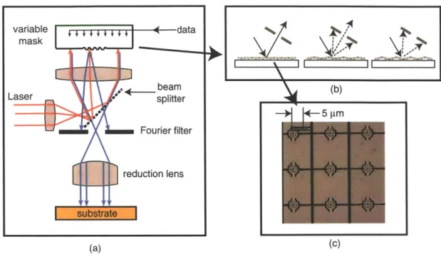
There are various forms of this variable mask. An example will illuminate this idea. A maskless lithography tool, currently being commercialized by Micronic Systems employs such a variable mask [4]. In their tool, the variable mask is used in a reflection configuration as opposed to the transmission configuration depicted in figure 1-6. The variable mask in their tool consists of an array of moveable micromirrors. A simplified schematic of the Micronic system is shown in figure 1-7(a). Light from a laser is directed onto the variable mask as shown. The variable mask is an array of micromirrors which can tilt about one axis. Since the micromirrors are close packed, appropriate tilts in the micromirrors can produce grating patterns on the mask. Light reflecting from these grating patterns gets redirected into diffraction orders as shown in figure 1-7(b). By controlling the tilt of the micromirrors on the variable mask, the intensity of the light directed into the zero order can be modulated. Only the zeroth diffraction order is allowed to pass through the Fourier filter and form pixels of the image on the substrate. Thus variable image formation is achieved through diffractive-spatial modulation of light. A scanning electron micrograph of the micromirror array is shown in figure 1-7(c). By scanning the substrate on a stage and by exposing overlapping fields, the entire substrate can be patterned accurately.
The optical projection system in the Micronic tool is very similar to that of a stepper. However, the size of the image projected onto the substrate is smaller than that used in an optical stepper. Larger images are built up by scanning the substrate and "stitching"
variable + data mask Laer...beam (b) Laser *splitter 5 gm Fourier filter reduction lens (a) (c)
Figure 1-7: Schematic of the Micronic Systems maskless lithography tool. (a) Full schematic.
(b) Working principle of variable mask. The mask is an array of micromirrors, which can
tilt about one axis to create a diffraction grating pattern on the mask. Light reflecting from this grating pattern gets redirected into diffraction orders. The height of the grating can be controlled by the tilt of the micromirrors and diffraction into the zero order can be controlled. Only the zeroth diffraction order is allowed to propagate past the Fourier filter and form pixels of the image on the substrate. (c) Scanning electron micrograph of the micromirror array. Note that the micromirrors are close packed and they can tilt about the vertical axis.
the smaller images. Off-axis illumination techniques can be used in this case to improve the resolution of printed features. However, the efficacy of these techniques tend to be very pattern dependent. Changes in the off-axis illumination require significant changes to the system. Therefore, off-axis illumination techniques effectively defeat the purpose of being able to print arbitrary patterns easily. Other resolution-enhancement techniques such as phase-shifting cannot be realized in such systems in a straightforward manner.
Variable mask systems are an evolutionary step towards maskless lithography from op-tical projection lithography. These have promise where maskless lithography is important. However, several key challenges still remain to be solved.
Scanning Spot Technology
As the name implies, this involves scanning a focused spot on the substrate to write arbitrary patterns. The substrate may also be scanned while the spot is held stationary or, both the substrate and the spot may be scanned. One example of such a system is the scanning-electron-beam-lithography system. The pattern to be printed is broken up into dots. The focused spot is then scanned over the location of the dots to build up the pattern dot by dot. This is illustrated in figure 1-8.
Binary Pattern Pixelated pattern Exposed Pattern
(x-y position in space)
Figure 1-8: Scanning Spot Maskless Lithography. (a) The binary pattern is drawn using
CAD software. (b) This binary pattern is broken up into dots. These dots represent the
positions in space where the focused spot must deliver dose into the resist on the substrate. (c) A fictitious final image in resist is depicted.
This is the most general form of maskless lithography in the sense that any arbitrary pattern can be composed of dots, the only limitation being the size of the dot itself. One can envision using resolution-enhancement techniques to improve the size and quality of the spot. This improved spot can then be used to write arbitrary patterns.
In general, there are several appealing features of a scanning-spot system. However, using a single spot to write an entire pattern makes this a very slow process. This is the single most important disadvantage of such a system. In this thesis, we explore a maskless lithography technique which aims to overcome this limitation by using a large number of focused spots to write in parallel. This technique is called Zone-Plate-Array Lithography (ZPAL).
Chapter 2
Introduction to Zone-Plate-Array
Lithography
Maskless lithography has grown in significance recently as research and industry leaders recognize its potential impact. Zone-Plate-Array Lithography (ZPAL) is a scanning-spot maskless lithography technique developed at the Nanostructures Laboratory at MIT. In this chapter, we provide a system-level description of ZPAL. The important components of the system are described as well.
2.1
System Description
ZPAL is a maskless lithography technique which uses an array of zone plates to create an array of spots on the substrate. A zone plate is a diffractive lens that focuses incident light into a spot. The light incident on each zone plate is controlled by a multiplexing element such as a spatial light modulator, where one pixel of the modulator controls the light incident on one zone plate. By scanning the substrate on a stage and properly timing the light modulation on each zone plate, arbitrary patterns are printed in a "dot-matrix" fashion. A schematic of the system is shown in figure 2-1.
Patterning using ZPAL involves breaking a large pattern into smaller "unit-cells". A unit-cell is that portion of the pattern, which one zone plate is responsible for writing. The
Focused Beamlet Zone -Plate Resist Wafer Scan Wafer
Figure 2-1: Schematic of a Zone-Plate-Array Lithography system. Light is incident on an array of zone plates. These zone plates, being diffractive lenses, focus light into an array of spots on the substrate. A multiplexing element (not shown here) controls light incident on each zone plate. By scanning the substrate on a stage, arbitrary patterns are printed in a
"dot-matrix" fashion.
unit-cell covers an area on the substrate directly beneath one zone plate'. At any instant, a zone plate writes one spot. Hence, within each unit-cell, the pattern is built up "spot-by-spot" by scanning the substrate. As will be shown later, each such "spot" can be very small and hence, high resolution patterning is possible. Moreover, since all the unit-cells are patterned at the same time, the trade-off between field-size and resolution is overcome. Thus, ZPAL combines the advantages of optical maskless lithography with the high throughput of a parallel-beam system.
The major components of a ZPAL system are depicted in figure 2-2. Light from a source is "cleaned" using a spatial filter and collimated before being directed onto the multiplexing device. Light from the device is then imaged onto the zone-plate array. Since the period of the pixels on the multiplexing device may be different from the period of the zone plates in the zone-plate array, magnifying optics may be required. The zone-plate array forms an array of spots on the substrate, which sits on a scanning stage. A central computer is responsible for synchronization of the motion of the stage and the pattern on the multiplexer. A prototype ZPAL system was built in the course of this research. The major components
'This is true when the zone plates are tight packed. In general, the unit-cell is the total area of the array divided by the number of zone plates.
of this system are discussed in detail next.
Radiation Source Beam shaping
Multiplexing Device
Texas InstrumentS DMDTM Silicon ht Machines-GLVi
Control Computer & Software 0& a
r=~
Iiii
Data Delivery&Boston
Maoachines SLMGray-Scale
Control
0F
Zone-Plate Array & Scanning Stage 0Zone
as U --Oate
R esi-4
a ter S can
Water
Figure 2-2: Schematic of the components of a ZPAL system.
2.1.1
Radiation Source
The wavelength of the radiation source is the defining factor for resolution in ZPAL. Since diffractive lenses exhibit strong chromatic aberrations, it is important that the source has sufficiently small bandwidth. The effect of the source bandwidth on lithographic patterning is discussed in chapter ???. The power of the source is one of the factors affecting throughput of the lithography system. Light from the source should be collimated in order to attain diffraction-limited focusing of the zone plates.
A helium-cadmium gas laser at a wavelength of 442 nm was initially used in the ZPAL system at MIT. Currently, the system uses a gallium-nitride diode laser at a wavelength of 400 nm. This laser is very compact (38mm by 144mm) and has very quick startup times compared to traditional gas lasers. In addition, the diode laser has an excellent temperature coefficient (quoted value is 0.05 nm/ C).
Figure 2-3: Photograph of the diode laser. This is the radiation source used in the ZPAL prototype built during the course of this research. This laser diode has a central wavelength
of
400nm
and a output power of 25mW. This laser module was manufactured by PowerTechnology, Inc [5].
2.1.2
Micromechanical Multiplexers
In ZPAL, the micromechanical multiplexer is a device comprising several pixels, such that one pixel controls the light incident on one zone plate. The rate at which all the pixels can be refreshed is an important factor in determining the patterning speed of the system. There is also an associated data delivery subsystem, which transfers the pattern data from the control computer to the multiplexing element. The rate of this data transfer is another factor affecting the patterning speed. In order to obtain good pattern fidelity, the intensity of light incident on each zone plate must be variable; this is called grayscaling. If real-time grayscaling is not possible, multiple passes over the same area of the pattern are required. This again affects the patterning speed of the system. In addition, the multiplexers must be compatible with the wavelength of the source. In this section, we briefly describe several candidates for the multiplexing element in ZPAL.
Texas Instruments Digital Micromirror Device (TI DMDTM)
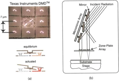
The TI DMDTM is an array of micromirrors [6]. Each micromirror can be independently activated by electrostatic forces. A scanning-electron micrograph of 9 micromirrors of this device is shown in figure 2-4(a). Each micromirror has electronics built directly beneath it. When not actuated, the micromirror is mechanically centered. When a voltage is applied between one electrode and the micromirror, electrostatic force causes the micromirror to tilt.
Mirror Incident Radiation 17 pam zl-equilibrium Zone-Plate e i Array actuated Substrate Stage (a) (b)
Figure 2-4: Texas Instruments Digital Micromirror Array. (a) Scanning electron micrograph
of the TI DMDTM. Note that the central mirror is removed to show the structure underneath. The mirror is hinged about one diagonal and is actuated electrostatically as shown in the bottom. (b) Schematic of the TI DMDTM being used in ZPAL. When the micromirror is not actuated, light is directed into the zone plate. Since the pitch of the micromirrors and that of the zone plates may be different, a telescopic system is required to transfer light from the micromirror array to the zone-plate array (not shown in this schematic).
in ZPAL. When the micromirror is in the "ON" position, light is directed into the zone plate.
When the micromirror is in the "OFF" position, light is directed away from the zone plate.
In this manner, "ON-OFF" states can be achieved. Grayscale control is achieved by using
the micromirror in a dynamic mode. The micromirror is driven by a pulsed signal which
alternates its state between "ON" and "OFF". By changing the duty cycle of the signal, the ratio of time the micromirror stays "ON" to the time it stays "OFF" can be controlled.
This, in turn, provides grayscale control of the light incident on the zone plate. This form
of "time-multiplexing" grayscale control, however requires more time to pattern every spot
and hence decreases patterning speed.
The TI micromirrors were initially used in the ZPAL system because of their early
com-mercial availability. Figure 2-5 show scanning electron micrographs of patterns written using
the TI DMDTM in a ZPAL system.
The TI device is packaged in a hermetically sealed glass case. This package is almost
opaque to all wavelengths below about 300 nm. This is a significant barrier to scaling the
Figure 2-5: Patterns written in parallel using the TI DMDTM. Scanning electron micro-graphs of patterns written in photoresist after development in a ZPAL system at A = 442 nm, and zone plate NA =0.7. This experiment was performed with a 3X3 array of zone plates. Hence 9 different patterns were written simultaneously.
system to lower wavelengths. In addition, the rate at which all the pixels could be refreshed is limited to about 10 kHz. As mentioned earlier, in order to attain diffraction-limited focusing, the wavefront incident on the zone plate must be a uniform plane wave. Since there is a small
indent at the center of each micromirror2, it is not very clear what the wavefront incident
on the zone plate might look like. Aberrations in this wavefront will translate into blurring of the focused spot.
Silicon Light Machines Grating Light Valve (SLM GLVTM)
The SLM GLVTM consists of a linear array of ribbons. Alternate ribbons are movable and
can be electrostatically actuated. A group of 6 ribbons are controlled in unison to form a
single pixel. A schematic of this device is shown in figure 2-6(a).
The working principle of the device is illustrated in figure 2-6(b). When the ribbons
are not actuated, light reflects in a specular manner. When alternate ribbons are pulled down, light sees a reflection grating and hence, diffracts into the ±1 and the 0 orders. The amount of light into each order depends on the height of this grating. When this height corresponds to a multiple of A/4 cos(O), then the light reflecting off the actuated ribbon and
ON All light into 0 order
0 Silicon Light Machines GLV TM
GRAY
+1
moveable ribbon
OFF
fixed All light into ± 1 orders
ribbon electrode
LX cos 0
t 4
(a) (b)
Figure 2-6: Silicon Light Machines Grating Light Valve. (a) Schematic of the GLVTM. The
device consists of a row of ribbons, of which a group of 6 ribbons composes one pixel (shown here). Alternate ribbons are moveable and can be electrostatically pulled down. (b) Cross-section through one pixel of the GLVTM. Top: The ribbons are not actuated. Incident light reflects totally into the 0 order. Center: Alternate ribbons are pulled down slightly. Incident light sees a reflection grating and some light gets redirected into the k1 orders. Bottom: Alternate ribbons are pulled down to completely extinguish the 0 order. All light is diffracted into the ±1 orders.
that reflecting of the fixed ribbon interfere destructively into the 0 order. Hence, all the light is switched into the ±1 orders. Thus, "ON-OFF" states and any states in between can be achieved or, in other words, the grayscaling capability is built into the device. This avoids multiple passes and hence, makes the patterning faster.
Figure 2-7 shows a simple schematic illustrating one configuration using the GLV as the multiplexing device in ZPAL. One pixel on the GLV controls the light incident on one zone plate. In this configuration, the 0 order light is used to illuminate the zone plate. The light efficiency is high but the "ON-OFF" contrast may not be very high due to spurious reflections which scatter light into the 0 order. On the other hand, if the +1 or -1 order is used to illuminate the zone plate, the "ON-OFF" contrast is maximized, but the light efficiency is lowered. There are optical techniques to collect both the
+1
and the -1 ordersto increase the light efficiency. Incident Radiation Zone-Plate Array Substrate Stage
Figure 2-7: GLVTM in ZPAL. One pixel on the GLVTM controls light incident on one zone
plate. In this configuration, the 0 order from the GLVTM is used to illuminate the zone plate. The higher diffraction orders are directed away by means of a fourier transform lens and a spatial filter, which are not shown in the figure.
Since the working principle of the GLV is based on diffraction, it is possible to use this device at shorter wavelengths. The actuation of the device involves a small displacement
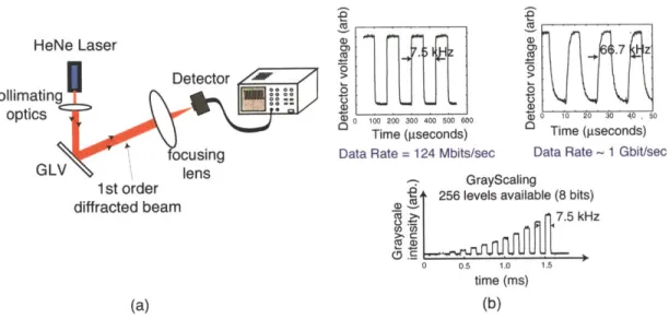
of the ribbons and therefore, the refresh rate of all the pixels can be quite high. This was experimentally verified in our laboratory. The experimental setup is illustrated in figure
2-8(a). A helium-neon laser (A = 633 nm) was used to illuminate the device. First order light
reflected off the device was collected by a lens and directed onto a detector. All the pixels on the device were turned "ON" and "OFF" at different frequencies and the signal on the detector was measured. The results are shown in figure 2-8(b). The top row is a plot of the detector signal as a function of time. The device worked reliably up to a refresh frequency of 67 kHz (beyond which the detector was unable to reliably measure the modulated optical signal). The plot on the bottom row indicates that real-time grayscaling is indeed possible at high speeds.
Since the GLV is a linear device, the number of spots projected onto the substrate is lower than when using a 2-D device such as a TI DMDTM. This adversely affects the patterning
HeNe Laser Detector collimating optics ocusing GLV lens 1 st order diffracted beam (a) CD 7.5 Vz.7 CD z 0
~
0 0 0100 20000400500600 000 10 20 30 40 .0Time (gseconds) 0 Time (paseconds)
Data Rate = 124 Mbits/sec Data Rate ~ 1 Gbit/sec
S 25GrayScaling
.2 256 levels available (8 bits)
7.5 kHz CZO CD~ .~ S _________ 0 0.5 1.0 1.5 time (ms) (b)
Figure 2-8: Experimental verification of the performance of the GLVTM. (a) Experimental setup. The data delivery system from the computer to the GLV is not shown here. (b) Top
row: Optical signal modulated by the GLV at 7.5 kHz and 66.7 kHz. Bottom: Optical signal
modulated in time and intensity (grayscaled) by the GLV.
speed due to the increased number of "turns" of the stage.3
Boston MicroMachines Spatial Light Modulator (BMM SLM)
The BMM SLM is an array of micromirrors which can move up and down in a piston fashion. An optical micrograph and a schematic of the device are shown in figure 2-9(a). Each micromirror is mechanically attached to a diaphragm by a post. The diaphragm and the substrate form a pair of electrostatic parallel-plate actuators. This device was invented at Boston University [7] and is currently being commercialized by Boston Micromachines [8]. This device is employed in an intereferometric manner in order to accomplish spatial light modulation. Light reflected from the device is interfered with a reference beam. If a micromirror is pulled down by A/4, light reflected off it will destructively interfere with its corresponding portion of the reference beam, producing a dark pixel. By pulling the micromirror down by heights between 0 and A/4, grayscale modulation of the pixel can be achieved. Thus, this device provides grayscaling while writing, which avoids multiple 3Most of the time is spent changing directions (or turning) while scanning. More turns are needed for a 1-D array of spots as compared to that for a 2-D array of spots.
B 14- reference mirror BMM SM
reference beam
incident beam
4,
beam-splitterElectrostatically zone-plate array actuated
diaphragm Attachment Mirror Pixel 4
Electrod Vsubstrate
stage
(a) (b)
Figure 2-9: Boston Micromachines SLM. (a) Top: Optical micrograph of a portion of
the device. Bottom: Schematic cross-section through the dashed line. Each mirror can be electrostatically actuated by means of electrodes below. (b)Working principle of the BMM
SLM in ZPAL. Light reflected from the micromirrors is interfered with a reference beam
as shown. When a mirror is pulled down by A/4, the reflected light is phase shifted by r with respect to the reference beam and that portion of the beam shows a dark pixel. One micromirror controls light incident on one zone plate. By controlling the heights to which the micromirror is pulled down, the intensity of light incident on the zone plate can be grayscaled.
writing passes. One pixel (micromirror) illuminates one zone plate. This working principle is illustrated in figure 2-9(b).
Since the on-axis reflected light is used in this configuration, spurious reflections from the device could reduce contrast between the "ON" and "OFF" states. Nevertheless, this is an attractive and simple solution if large-pixel-count devices at high refresh rates become commercially avaliable.
Microshutters
All the multiplexers discussed so far are reflective or diffractive in their function. These devices scatter light and therefore, reduce contrast between the "ON" and the "OFF" states. Moreover, they will not operate at shorter wavelengths such as EUV (13 nm) or X-ray, since
materials with sufficient reflectivity are not readily available4. In order to address these
disadvantages a multiplexer that works by transmission is required.
4
Although glancing angle reflection is still possible at these wavelengths, this presents challenging design issues for the system.
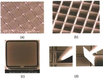
Such a device, comprising an array of microshutters, is being developed for astronomical applications at the NASA Goddard Space Flight Center [9]. Each pixel on this device consists of a silicon nitride membrane shutter attached to a frame by a torsion beam. The shutter is capable of opening 90 degrees out of the plane of the device by rotating about the axis of the torsion beam. Scanning electron micrographs of this device are shown in figure 2-10.
(a) (b)
(c) (d)
Figure 2-10: Microshutter arrays being developed at NASA. (a) Scanning electron
micro-graph of an array of microshutters. (b) Backside of the array showing the support structures. (c) Single microshutter. (d) The microshutter being actuated manually using a micromanip-ulator. The shutter hinges about the torsional hinge and can rotate 90 degrees out of the plane of the array. Note that each microshutter is about 100pIm x 100pim in dimension.
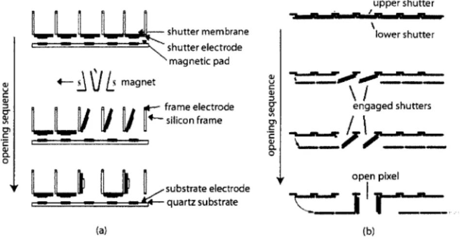
Two methods of actuation for this device has been proposed. The first method uses a combination of magnetic and electrostatic methods. A moving electromagnet beneath the microshutter array produces a force on a magnetic pad on the microshutter causing it to bend out of plane. An electrode on the frame of the microshutter, when actuated holds the microshutter open. The microshutter array is placed in close proximity to a transparent substrate which has an array of electrodes aligned to each microshutter. Voltage applied to
an electrode holds the corresponding microshutter closed while the magnet is scanned. The operating sequence is illustrated in figure 2-11 (a). The second method involves mechancal and electrostatic actuation with a double shutter mechanism. Two arrays of microshutters are aligned to each other and brought in close contact. Microshutters on both arrays have