Design of the high-speed framing, FEC, and
interleaving hardware used in a 5.4km
free-space optical communication experiment
The MIT Faculty has made this article openly available.
Please share
how this access benefits you. Your story matters.
Citation
Greco, Joseph A. “Design of the high-speed framing, FEC,
and interleaving hardware used in a 5.4km free-space optical
communication experiment.” Free-Space Laser Communications IX.
Ed. Arun K. Majumdar & Christopher C. Davis. San Diego, CA, USA:
SPIE, 2009. 746409-7. © 2009 SPIE--The International Society for
Optical Engineering
As Published
http://dx.doi.org/10.1117/12.826309
Publisher
The International Society for Optical Engineering
Version
Final published version
Citable link
http://hdl.handle.net/1721.1/52731
Terms of Use
Article is made available in accordance with the publisher's
policy and may be subject to US copyright law. Please refer to the
publisher's site for terms of use.
Design of the High-Speed Framing, FEC, and Interleaving Hardware
Used in a 5.4km Free-Space Optical Communication Experiment
Joseph A. Greco
Massachusetts Institute of Technology Lincoln Laboratory, Lexington, MA 02420-9108
ABSTRACTThe forward error correction (FEC) and interleaver realizations used in a 5.4 km horizontal-path link experiment incorporated several unique elements that were specifically tailored to address turbulence-induced fading. To facilitate optimization studies, this hardware was designed to afford a high degree of flexibility in the FEC code structure and interleaver length. An essential aspect of this structure was the standards-compliant client interface, which provided seamless connectivity to fiber-based terrestrial networks. Through the use of an OTU1 (2.667 Gbaud) architecture with nonstandard interleaving, error-free transmission was achieved in the presence of strong scintillation that produced fade events that frequently exceeded 10 ms in duration.
This work was sponsored by the Department of Defense, RRCO DDR&E, under Air Force Contract FA8721-05-C-0002. Opinions, interpretations, conclusions and recommendations are those of the authors and are not necessarily endorsed by the United States Government.
Keywords: forward error correction, symbol interleaving
1.
INTRODUCTION
The complex fading behavior of free-space optical communication links introduces a unique set of engineering challenges, particularly at the hardware interfaces to terrestrial networks functioning under standard data transfer protocols. The optical transport network (OTN) protocols that have been in use since 1996 provide for a variety of forward error correction (FEC) formats, but error correction alone is not sufficient when the received signal may drop below the detection threshold for periods as long as 10 msec.
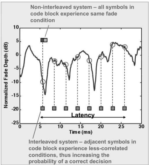
Forward error correction introduces a degree of data redundancy, which allows a transmitted codeword to be correctly interpreted despite the loss of a significant fraction of the individual codeword elements. This can be effective on a link where the bit errors are randomly distributed, rather than bursty. On a free-space optical link, the received power can vary over tens of dB (fading), with fades lasting on the order of a millisecond or longer. As indicated in Figure 1, a fading event that is much longer than the codeword duration will usually result in an unrecoverable loss of information. The concept of symbol interleaving was developed to overcome the bursty, non-uniform distribution of errors that occur in a fading channel that fluctuates slowly with respect to the codeword transmission time. In essence, each codeword is disassembled, with the individual symbols transmitted with a temporal spacing that is comparable to the duration of a channel fade, and then reassembled in the proper order at the receiver. To match the input data rate, the incoming bytes are rearranged and interleaved so that a steady byte stream is maintained. Thus, the channel data rate is unaffected by this process, but the errors are redistributed such that there is a high likelihood that each codeword can be correctly decoded and reconstructed. The most significant drawback of this construct is the latency that is introduced due to the codeword symbol spreading. This delay will be equal to the product of the symbol transmission interval and the number of symbols per codeword.
Forward error correction, combined with symbol interleaving, represents a critical enabling technology for free-space optical communication links. Although the theoretical improvements that this approach affords have been quantified in the literature, to the best of our knowledge the MIT-LL 5.4 km horizontal path experiment represents the first successful demonstration of a real-time, line rate, hardware implementation that incorporates a client OC-48 interface and an OTU1 (2.667 Gbaud) protocol interface with nonstandard interleaving over a free-space optical link.
Fig. 1. In a slowly-fluctuating fading channel every byte of a codeword may be incorrectly interpreted by the receiver, in which case error correction is impossible. Forward error correction combined with interleaving distributes the components of each word over a longer period of time, thereby increasing the likelihood that the information will be corrected decoded at the receiver.
2.
REDUCTION OF LATENCY WITH CONVOLUTIONAL INTERLEAVING
When developing hardware that is to carry network traffic that can be time sensitive (TCP/IP acknowledgements or other time synchronous traffic) consideration must be given to the overall system latency that is added by the (de)interleaver pair.
Two types of interleaver realizations were considered, block and convolutional. A traditional block (de)interleaver has an overall latency of 2*T where T is the depth in time of either the interleaver or deinterleaver. This is due to the fact that both the interleaver must be fully filled before reordered data can be transmitted and the deinterleaver must be fully filled before properly reordered symbols are present on its output.
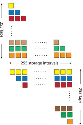
Fig. 2. Depiction of delay structure of convolutional interleaver (top) and deinterleaver (bottom). (De)interleaver is implemented as a tapped delay line structure. Vertical axis depicts interleaver taps, corresponding to symbols within a codeword (jth symbol of each codeword is assigned to jth tap). Horizontal axis represents number of discrete delay units. Unit delay is software loadable.
A convolutional (de)interleaver shown in Figure 2 has ~1/2 the latency of a traditional block interleaver of the same depth. This is due to the fact that the convolutional interleaver does not need to be completely filled before beginning to transmit interleaved symbols. The interleaver begins to transmit symbols on the channel after one unit delay (D). For codewords of duration n symbols, this is matched against the deinterleaver dimension (n*D) to return deinterleaved symbols to the system for an overall latency (n+1)*D. This is only slightly in excess of the depth of the interleaver D.
3.
DESCRIPTION OF ENCODING AND INTERLEAVING HARDWARE
A fundamental tenet when developing the hardware described here was to implement standards based interfaces. The motivation for this was that this hardware would allow for COTS networks to be transparently (increased latency) transported over free space optical links. This requires all processing, encapsulation, FEC, and interleaving to operate at line rate. The standards supported by this hardware are interleaved OTU1 on the free space interface and Gigabit Ethernet (GbE) , SONET (OC-12, OC-48) on the client interface for the 2.5G family of rates. Additionally, client interfaces of OC-192 and 10GE-WAN with interleaved OTU2 on the free space interface for the 10G rate families are currently supported on the same hardware.
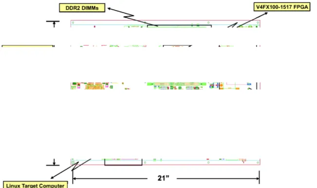
The High speed FEC and Interleaver Card (HFIC) is the hardware realization of this concept. The HFIC is based on Xilinx Virtex4 FPGAs and COTS DDR2 DIMMs. A common design allows for a two board set to realize the functions necessary to electrically mitigate the effects of the free space channel. Each HFIC contains 3 Virtex4FX100 FPGAs, 2
MSA300 telco standard interface supporting SFI4 signaling, 8 DDR2-266 DIMMS, SONET-compliant phase-locked loops (PLLs), power generation, and a COTS single board computer (SBC) running a soft real-time UNIX operating system.
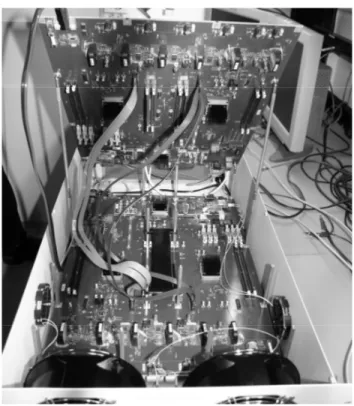
Figure 3 depicts the two HFIC set and the location of the functions realized in the associated FPGAs. The two boards are referred to as the client and the network. The client HFIC interfaces to COTS terrestrial network and the network HFIC interfaces to the free space channel. Figure 4 shows highlights of an individual HFIC. Figure 5 is a photograph of the HFIC chassis with a set of two HFICs.
.
Fig. 3. Depiction of dual-HFIC configuration used for electrical channel mitigation. Client interfaces on the left (West). Free-space channel interface on the right (East, Optical Modem Group).
Fig. 5. Photograph of HFIC chassis housing two HFICs. Upper HFIC raised for viewing purposes. Network card on top. Client card on bottom.
3.1 Client HFIC
On the client HFIC FPGA #1 contains the desired client interface and ITU G.709 compliant OTN encapsulation with the FEC area padded out on the egress data stream. On the ingress data stream, the FEC area is dropped and the payload is decapsulated from the OTN data stream before presenting the data to the client interface.
FPGA #2 on the client HFIC only processes the egress data stream and this is where FEC encoding is performed. Currently G.709 standard FEC, Reed Solomon RS(255,239) is implemented. This code uses 8-bit symbols, 16 parity symbols per codeword, and a total of 255 symbols per codeword. The error correcting capability of this code is 8 symbols per codeword with hard decision decoding, as implemented. Similarly, FPGA #3 accomplishes the corresponding RS(255,239) FEC decoding and error correcting on the ingress data stream.
3.2 Network HFIC
On the network HFIC FPGA #1 is largely bypassed, in that it just moves the interleaved OTN data stream to/from the MSA300 transponder interface supporting the free space channel. The one notable function performed in this FPGA is the framing function on the interleaved OTN data stream received from the free space channel. The framing function is one of finding the Frame Alignment Signal (FAS) and aligning the bytes for subsequent deinterleaving. G.709 specifies that the FAS must be detected 3 times to declare alignment and missed 3 consecutive times to be declared out of alignment. While this is reasonable on a fiber based channel, the duration of fades on a free space channel will regularly be greater than 3 times the frame period at OTU1 (48.971μs) making the detection of FAS not possible in a fade. As such, in this hardware we implement a modified frame alignment algorithm in that we declare in frame after 3 consecutive FAS matches, but allow for tuning in the form of a software loadable hardware register, that specifies the number of consecutive missed FAS before declaration of out of frame (OOF). Typically, the value loaded slightly exceeds the longest fade duration divided by the frame period.
FPGA #3 & #2 implement the interleaver and deinterleaver. A common design is used for both the interleaver and deinterleaver. A convolutional interleaver design was chosen rather than a block interleaver design because of the 2x
reduction in both memory requirements and latency. The basic structure of the interleaver is depicted in Figure 2. Each square represents a delay element of duration D. Remembering that there are 255 symbols in each codeword of an OTN frame, this sets the number of taps of the interleaver to 255. Each tap will see the corresponding symbol number from all codewords in a frame. For example, the 3rd tap, shown in red, will see the 3rd symbol from each of the 64 codewords in each frame. The nth tap has n delays, forming a lower triangular matrix. The total interleaver span, which is the maximum tap delay, is T = 255*D. This has the side benefit of enabling the FAS to pass through the interleaver unperturbed, allowing for the standard frame alignment algorithm to operate in the free space channel. However, as mentioned above, a modified frame alignment algorithm, specifically tailored to the fading channel, is employed on the free-space channel interfaces. The tap table is software-loadable through the single-board computer (host) resident on each HFIC. This enables one hardware design to implement a number of different interleaver spans, from a minimum of 255 times the frame period to the maximum memory in bytes divided by 16320 bytes per frame, times the frame period (OTU1 48.971 microseconds, OTU2 12.191 microseconds).
Complementary to the interleaver, the deinterleaver forms an upper triangular matrix of taps and delays. The same tap table used for the interleaver is loaded in reverse order by the host to become the deinterleaver. For example, the jth symbol in a codeword experiences a j*D delay in the interleaver and a (256-j)*D delay in the deinterleaver, so that each symbol experiences a net delay of 256*D, reconstituting each codeword and frame.
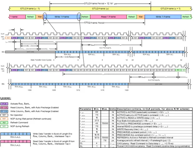
The interleaver and deinterleaver structures can be implemented using COTS DDR2 DIMMs. Figure 6 illustrates DDR2 bus access timing relative to OTU2 frame timing, with an expansion of the WRITE portion. READs follow a similar access methodology. It is worth noting that a memory bandwidth doubling over the data rate is required due to the fact that 16320 bytes must be written (equivalent of one OTN frame) and 16320 bytes must be read from memory within a single frame period. Using these methodologies, OTU2 streams can be (de)interleaved with memory operating at 174MHz SDR, 348MHz DDR on the 64-bit-wide DIMM data bus. These speeds are not difficult to achieve today. Currently available COTS DDR2 modules can operate at 800MHz. The HFIC concept was conceived in 2004 when these speeds were challenging to achieve using FPGA-based controllers.
FAS, which serves as the frame alignment marker in the OTN standard, is also used as the (de)interleaver alignment marker. FAS is used for synchronizing the interleaver in that it specifies which symbol is assigned to the first tap. Since, as mentioned above, FAS is preserved through the interleaver, it also serves as an alignment marker for the deinterleaver.
o Obes w vmio 069Q Co flu w vruo Me CO00 ECEVD ELSWS bSt ELSWS bSt
D escr ip t io n ( cr it er ia, in C LK p er io d s, f o r ab o ve R / W scheme) : ACTIVE to ACTIVE (same bank) command ( = 32·tC K)
ACTIVE bank a to ACTIVE bank b command ( = 4·tC K)
ACTIVE to READ or WRITE delay ( = 4·tC K)
Four Bank Activate period ( = 16·tC K)
ACTIVE to PRECHARGE command ( = 12·tC K)
Internal READ to precharge command delay ( = 2·tC K)
WRITE Recovery time ( = 4·tC K)
PRECHARGE command period ( = 4·tC K)
PRECHARGE ALL command period ( = tR P + tC K)
REFRESH to Active or Refresh to Refresh command interval Average periodic refresh interval ( = Framelength (µs) / 2) CAS Latency: Read Command to Data delay (tC K = 3.75 ns)
Posted CAS Additive Latency: Read Command pipeline delay (programmable)
tR E FI 7.8 µs tR FC 127.5 70000 ns AL 1 3 tC K CL 4 tC K tR P A 18.75 ns tR P 15 ns tW R 15 ns tR T P 7.5 ns tR A S 45 70000 ns tFA W 37.5 ns tR C D 15 ns tR R D 7.5 ns tR C 60 ns
Par amet er M in. M ax. U nit s
Fig. 6. Timing diagram for DDR2 bus accesses relative to OTU2 frames. Expansion of WRITE portion. DQ represents the data bus on the DIMMs. Addr Cntrl = Address Control.
4.
SUMMARY
Modular FPGA-based boards have been developed to realize electrical mitigation of free-space optical channel fading, compatible with terrestrial network standards. In particular, the boards implement client framing, ITU-T G.709 compliant OTN (OTU1 and OTU2) encapsulation and decapsulation, Reed-Solomon encoding and decoding, and nonstandard (de)interleaving. Client framing includes SONET (OC-48 and OC-192) and Ethernet (GbE and 10GE-W). This hardware was demonstrated in field tests during September 2008 over a 5.4 km horizontal link and further validated in subsequent laboratory test
s.
5. THANKS
This hardware realization effort was the work of the High Speed Electronics (HSE) design team. Without their collective efforts this realization would not have been possible. Many additional thanks to Dr. John D. Moores and Dr. Ronald R. Parenti for insightful comments and preparation of this manuscript.