HAL Id: hal-00569713
https://hal.archives-ouvertes.fr/hal-00569713
Submitted on 25 Feb 2011HAL is a multi-disciplinary open access archive for the deposit and dissemination of sci-entific research documents, whether they are pub-lished or not. The documents may come from teaching and research institutions in France or abroad, or from public or private research centers.
L’archive ouverte pluridisciplinaire HAL, est destinée au dépôt et à la diffusion de documents scientifiques de niveau recherche, publiés ou non, émanant des établissements d’enseignement et de recherche français ou étrangers, des laboratoires publics ou privés.
TEM characterization of oxidized AlGaAs/AlAs
nonlinear optical waveguides
E Guillotel, Cyril Langlois, F Ghiglieno, G Leo, C Ricolleau
To cite this version:
E Guillotel, Cyril Langlois, F Ghiglieno, G Leo, C Ricolleau. TEM characterization of oxidized AlGaAs/AlAs nonlinear optical waveguides. Journal of Physics D: Applied Physics, IOP Publishing, 2010, 43 (38), pp.385302. �10.1088/0022-3727/43/38/385302�. �hal-00569713�
TEM characterization of oxidized AlGaAs/AlAs
nonlinear optical waveguides
E. Guillotel, C. Langlois*, F. Ghiglieno, G. Leo and C. Ricolleau
Laboratoire Matériaux et Phénomènes Quantiques, CNRS-UMR 7162
Université Paris Diderot – Paris 7
Case courrier 7021, 75205 Paris Cedex 13, France
Abstract
The internal interfaces of multilayer AlxGa1-xAs/AlAs nonlinear optical waveguides are
investigated by high-angle annular-dark-field and energy-filtered scanning transmission electron microscopy, before and after partial wet oxidation of AlAs layers. Via a simple phenomenological model, the corresponding roughness parameters allow predicting the scattering-induced waveguide optical losses, which are in reasonable agreement with the experimental value of 0.5 cm-1. We also find that AlxGa1-xAs layers adjacent to oxidized AlAs
tend to be oxidized through the interfaces, even for low Al fraction, with typical oxidation depths of 9 nm for x=0.7 and 2 nm for x=0.
*
Corresponding author:[email protected]
I. INTRODUCTION
The near- and mid-infrared (NIR and MIR respectively) domains are of great interest for spectroscopy, since a huge number of molecules have their fundamental rotational-vibrational resonances in these spectral ranges. While the ideal source for this kind of applications should be continuous-wave (cw), continuously tunable, cheap and easy to use, the current state of the art includes semi-conductor lasers and optical parametric oscillators (OPO's) [1]. Although the former can provide significant cw output power at almost any wavelength from visible to 20 µm, their overall tuning range is typically limited to a few tens of nanometers and is commonly affected by longitudinal-mode hops. The latter, conversely, are easily tunable on several micrometers, but they are neither compact nor cheap, and seldom practical. OPO's rely on the χ(2) optical properties of non-centrosymmetric materials, and namely on cavity oscillations triggered by spontaneous parametric down-conversion (SPDC).
In SPDC, an intense “pump” wave at frequencyωp gives rise to a "signal" wave atωsand an
“idler” wave ωi, with ωs + ωi = ωp, provided that the so-called phase-matching (PM)
condition is fulfilled, reflecting the need that the three waves stay unmodified in their initial phase relation. The PM is often achieved by compensating crystal dispersion with optical birefringence, or by periodically reversing the sign of χ(2) along the propagation path. While uniaxial ferroelectrics like lithium niobate (LiNbO3) have long been the most popular crystals
for nonlinear sources, today gallium arsenide (GaAs) is considered as a serious option because of its larger χ(2), its mature technology development, and its full optoelectronic integrability [2,3].
Since GaAs is neither birefringent nor ferroelectric, it only became feasible for practical χ(2) optics after the controlled fabrication of a stable aluminum oxide (AlOx) was demonstrated in the early 90's [4], with the subsequent development of form birefringence in GaAs waveguides [5]. Since then, several three-wave mixing interactions were demonstrated in
AlGaAs/GaAs/AlOx waveguides [6-9], including SPDC.Despite those encouraging results, the goal of a semiconductor integrated OPO has not yet been reached because of the 0.5 cm-1
optical losses that occur after AlAs selective oxidation [8], a factor-of-five higher than the guided-wave losses before oxidation. Although light scattering in such waveguides has long been observed and tentatively ascribed to GaAs/AlOx interfaces roughness [10], the only transmission electron microscopy (TEM) related study so far was only of a qualitative type [11]. Because of the TEM potential in quantitative analysis at the atomic scale, this article reports on a TEM study aimed at quantifying the GaAs/AlOx interfaces roughness and evaluating the related optical losses. TEM analysis has also helped us investigating other possible optical losses sources linked to oxidation like absorbent centers or volume scatterers.
Hereafter, we confirm that the selective wet oxidation of GaAs/AlGaAs nonlinear waveguides is responsible for a deterioration of the interfaces, their roughness increasing fromσ=0.37 nm before oxidation to σ=0.53 nm (lower bound) after oxidation. The scattering-induced optical loss due to the interface roughness is evaluated with a model that leads to a coefficient of 0.3 cm-1, in reasonable agreement with the experimental value of 0.5 cm-1 induced by the
oxidation process in GaAs/AlOx waveguides. The formation of an intermediate oxidized GaAs layer is also identified and finally the formation of γ-Al2O3 nanocrystals embedded in
an amorphous AlOy(a-AlOx) layer is observed. The additional interfaces created by these two
alumina phases, as well as the presence of scattering nanocrystals, could be responsible of supplementary propagation losses.
II. EXPERIMENTAL DETAILS
The samples are 3 mm-long GaAs/AlOx waveguides designed for type-I SPDC. They allow the conversion of a pump beam with wavelength λp 1.03µm into one signal and one idler
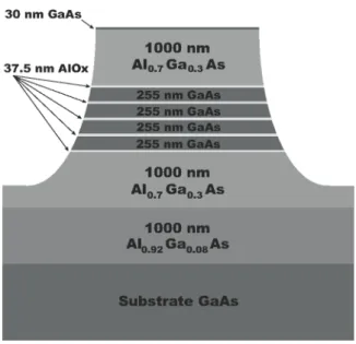
photons, the wavelengths of which can be set in the 1.2 - 4.2 µm range. The vertical structure, grown by molecular beam epitaxy [12], is the following: GaAs-substrate / 1000 nm Al0.92Ga0.08As / 1000 nm Al0.7Ga0.3As / 37.5 nm Al0.98Ga0.02As / 4x(255 nm GaAs / 37.5 nm
Al0.98Ga0.02As) / 1000 nm Al0.7Ga0.3As / 30 nm GaAs. All ternary alloys are digital alloys
grown by alternating a few monolayers of GaAs and AlAs in order to obtain the targeted stoichiometry. Lateral confinement of the propagating waves is achieved by 3 µm-wide and 2.8 µm-high guiding ridges, which are chemically etched with a HBr:CH3COOH:Cr2K2O7
solution. Waveguides are oriented along the [110] direction in order to optimally exploit the only nonzero component, χxyz, of itsχ(2)tensor. Al0.98Ga0.02As (referred to as AlAs afterward)
layers are then selectively transformed into AlOx through lateral wet oxidation [13]. This is done by heating the samples for 14 min at 420°C in a quartz furnace saturated by H2O vapor
transported by 2 L/min N2carrier gas passing through a H2O bubbler at 70°C. The structure is
shown in figure 1.
Cross-section TEM thin foils were prepared by Ar+ ion milling using a JEOL Ion Slicer
system at 8 kV gun voltage for 1 hour, ending by a 2 kV step of 2 min to get rid of the surface amorphous material formed during the process. Thin foils were analyzed by several TEM techniques on a JEM 2100F TEM equipped with field emission gun operating at 200kV, a Gatan imaging filter and a CCD camera. GaAs/AlOx interfaces were characterized by high angle annular dark field (HAADF) scanning TEM (STEM) with a Gatan detector. This technique is sensitive to atomic number Z with a 0.2 nm spatial resolution. Chemical maps were obtained by energy filtered TEM (EFTEM) using the three window technique with an energy slit of 20 eV width for the acquisition of two pre- and one post-edge images around
the oxygen K edge. Elemental distribution images were then displayed as the difference between the post-edge image and its background signal extrapolated from the two pre-edge images [14]. In this technique, elemental concentrations are proportional to the intensity in the resulting chemical map. Finally, the structure of AlOx was determined by acquiring high resolution TEM (HRTEM) images with a Gatan Ultrascan 4000SP CCD camera.
III. RESULTS AND DISCUSSION A. Interfaces roughness characterization
For the roughness characterization of the interfaces, the HAADF-STEM technique has been preferred to HRTEM because the latter suffers from interference delocalization at interfaces when operating near the Scherzer defocus due to the spherical aberration of the objective lens [15], which results in a lower precision in determining the interface position.
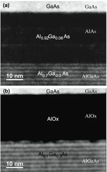
A series of HAADF images of the topmost AlAs layer was acquired for a non-oxidized and an oxidized samples. The topmost layer is placed between an Al0.7Ga0.3As (hereafter referred to
as AlGaAs) layer on one side and a GaAs layer on the other side. All the interfaces in the guiding core (GaAs/AlAs, AlGaAs/AlAs, GaAs/AlOx and AlGaAs/AlOx interfaces) have been characterized. Since Ga appears only on one side of these interfaces, their position can be precisely determined by the chemical contrast of HAADF images resulting from Ga concentration. In order to maximize the statistical information, successive images have been acquired along the layers over about 700 nm for both samples, with similar imaging conditions. This was made possible by the almost constant thickness of the thin foils on the observed area, according with the preparation instrument specifications. Figure 2 shows an example of those images for the non-oxidized sample and for the selectively oxidized sample. The most remarkable difference between the two images is the important modification of the AlGaAs/AlAs interface when it turns into AlGaAs/AlOx. Conversely, the GaAs/AlAs
interface aspect does not seem to evolve appreciably after oxidation, as we will discuss in detail hereafter.
To accurately measure the roughness amplitude at the interfaces, the following procedure has been set: (I) image recombination, (II) contrast enhancement, (III) images thresholding, (IV) search of boundary coordinates, (V) linear slope determination of the boundary, (VI) slope removal and (VII) histogram analysis.
Image recombination (I) relates to the assembling of the complete series of adjacent HAADF images to form a single image. This was done by acquiring successive slightly overlapping images of the thin foil, paying attention to specific common details in two contiguous images. The contrast of the resulting image was then optimally set in order to get the central layer as dark as possible and the adjacent ones as bright as possible (II). This step is critical as we do not want to miss small interface details. The thresholding of the image (III) consists in converting all pixels which an intensity level below (above) a given intensity threshold to 0 (1). During the thresholding we also payed attention to misinterpretation of the true pixels level, in particular at the boundary. Indeed, in a specific row a sequence of pixels of intensity level close to the threshold may be alternatively converted in 0 and 1 digits. In this case the interface is not correctly defined. To prevent such phenomenon, a minimum number of successive pixels of same value (0 or 1) has been fixed to validate the interface position. Search of boundary coordinates (IV) is then employed through an algorithm that scans the digital image rows one by one. This algorithm locates the transition from 0 to 1 for each column and associates the corresponding coordinates to the interface position, in the reference frame of the image. Afterward, (V) to obtain an interface parallel to the x axis, the slope of the boundary position curve is fitted with linear least squares and (VI) removed from the curve. Finally (VII), the data are treated to form a histogram of all the curve values. The
interface roughness can then be precisely measured by determining σ,the width at half-maximum (HWHM) of a Gaussian function fitted to the histogram data.
Such methodology has been carried out for the non-oxidized and the oxidized sample images. The raw average value for the non-oxidized sample is σ=0.17 nm for both GaAs/AlAs and AlGaAs/AlAs interfaces. In the case of the oxidized sample, σ1=0.40 nm for the GaAs/AlOx
interfaces andσ2=0.48 nm for the AlGaAs/AlOx interfaces. Considering the smoothing effect of the interfaces profile due to the finite foils thickness, these values are underestimated. Following the results obtained by Goodnick et al. [16], we corrected them into: σ=0.37 nm,
σ1=0.53 nm andσ2=0. 69 nm.
In order to evaluate the scattering-induced attenuation coefficient α associated to such parameters, we have adapted Lacey and Payne's model [17] to our multilayer structure, as we will detail in a future communication. The main idea is to determine the roughness amplitude
σand the coherence length Lcof the interface profile f(x) through the autocorrelation function of the interface profile, R(u)=<f(x)f(x+u)>.σand Lccorrespond to R(0) and to the HWHM of a Gaussian fit of R(u) respectively and are directly linked to the attenuation coefficient. αwas found to be about 0.3 cm-1 which is in reasonable agreement with the experimental value of
0.5±0.2 cm-1.
B. Chemical and micro-structural characterization
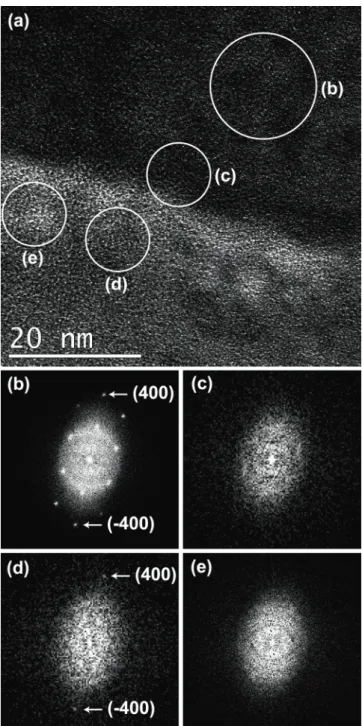
The structure of the interfaces have been investigated by HRTEM imaging. Figure 3(a) shows a HR image of a GaAs/AlOx interface. GaAs, on the upper side of the picture, is clearly mono-crystalline as suggested by the power spectrum (PS) of region (b), exhibiting spots that are characteristic of {200}, {111} and {400} planes of GaAs. At the boundary between dark and bright parts of the picture, the PS of region (c) suggests that the GaAs becomes
amorphous. It is worth noting that according to its contrast the bright side of the picture is supposed to correspond to AlOx as shown in figure 5. However, the PS of region (d) exhibits spots corresponding to the {400} plane of GaAs. The PS of region (e) reveals the presence of an amorphous material.
These results show that GaAs gets oxidized during the selective oxidation of Al rich layers. It must not be confused with lateral wet oxidation for which AlxGa1-xAs layers with x<0.7
cannot be oxidized [18]. It is rather that oxidation of GaAs takes place through the interfaces as a consequence of lateral wet oxidation of the AlAs layers. This hypothesis is supported by the residual presence in the bright side of the boundary of poorly oxidized GaAs (region (d)) surrounded by amorphous material (regions (c) and (e)). The contrast modification of dark to bright is ascribed to the substitution of As elements of GaAs by O, which modifies the electrons scattering conditions.
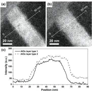
In order to better understand the oxidation effects in the device, a chemical characterization of the layers has been carried out by EFTEM imaging. Elemental maps of O were acquired from two types of layer stackings: GaAs/AlOx/GaAs (hereafter referred to as type 1) and GaAs/AlOx/AlGaAs (referred to as type 2). Results are shown in figure 4. Figure 4(a) is an EFTEM map of a type 1 AlOx layer acquired with an energy window set around the oxygen K edge. Figure 4(b) shows the O map for a type 2 AlOx layer acquired in the same experimental conditions. In these images O-rich regions appear brighter. In both pictures an intensity profile has been extracted along a line parallel to the growth direction and averaged on about 30 nm along the interface. The FWHM of these profiles, reported in figure 4(c), is 39nm and 45 nm in the case of type 1 and 2 AlOx layer respectively. From the HAADF images of figure 2 the thickness of the AlOx layer has been measured based on the presence of Al, which appears dark in the middle of the images. A thickness of 34 nm was found for type-I and type-II AlOx layers. From the difference between the measurements obtained from
EFTEM and HAADF images, it can be deduced that the neighboring layers of the AlOx layer get oxidized from the interfaces. In the case of type 1 stacking, both these GaAs layers are oxidized over a thickness t = (39 - 34)/2 = 2.5 nm. In the case of type 2 stacking, the GaAs layer is still oxidized in the first 2.5 nm, which leads to the conclusion that the AlGaAs layer is oxidized in the first (45 - 34) - 2.5 = 8.5 nm. It is evident that an oxidation process occurs from the AlOx layers interfaces, thus confirming the HRTEM observations: the richer in Al the deeper an AlGaAs layer is oxidized.
Finally, we have characterized the microstructure of the AlOx layers. According to HAADF images presented in figure 1, 37.5 nm-thick AlAs layers are only 34 nm-thick after oxidation, corresponding to a 10 % contraction. This is a very common phenomenon in lateral wet oxidation [11, 19] associated to the formation of polycrystalline grains of γ-Al2O3 in an
amorphous AlOx(a-AlOx) matrix. It is explained by the reduction of the volume by Al atom
inγ-Al2O3(2.85 Å3) relative to the case of AlAs (3.57 Å3) [20].
Taking into account that for pure a-AlOx such contraction is not observed [21], one can therefore suppose the presence of crystalline grains in the AlOx layers. HRTEM observations of AlOx layers have been carried out at high magnification (1.1 106 X). A typical image is
shown in figure 5, where the dark parts in the upper right and lower left corners correspond to GaAs, whereas AlOx appears as bright in the rest of the picture. A close look at the image allows one to distinguish crystallized regions oriented along different directions.
In order to identify the nature of these regions, a PS of the whole image has been computed and shown in the upper left inset. Several characteristic spots appear in this PS, which tend to form circles typical of fully polycrystalline materials. The d-spacing corresponding to each of these spots has been measured, confirming the presence ofγ−Al2O3grains (the corresponding
are missing, e.g. those of {222} or {422} planes, mainly because of their low diffracting intensity.
Identification of the positions and sizes of several grains was possible through Fourier filtering of the image, using only one of the diffraction spots for a single grain. They are visible as superpositions on the original HRTEM image (figure 5). Most of them have a size in the range from 10 to 20 nm and are quite gathered in the middle of the amorphous AlOx layer. The effect of these grains on additional scattering losses can be neglected due to the negligible index contrast between AlOx andγ−Al2O3.
IV. CONCLUSION
We have carried out a TEM study of the effects of selective oxidation on GaAs/AlAs nonlinear waveguides. Comparison of non-oxidized and oxidized samples reveals a roughness increase of 43% and 86% for GaAs/AlAs and AlGaAs/AlAs interfaces, respectively. Such roughness has been associated to a scattering-induced attenuation coefficient about 0.3 cm-1 in
reasonable agreement with the experimental measurements of 0.5 cm-1 induced by the
oxidation process. Chemical characterization of the oxidized AlAs layers indicates the oxidation of its neighboring AlGaAs layers through the interfaces. The richer in Al the deeper they get oxidized. Finally, the morphology of the AlOx layer has been identified as being composed ofγ-Al2O3polycrystalline grains embedded into an amorphous AlOx matrix.
We are thankful to the région Ile-de-France for financial funding and for convention SESAME 2000 E1435 for the support to cryo-electron microscope JEOL 2100F installed at IMPMC UMR 7590.
REFERENCES
[1] I. T. Sorokina and K. L. Vodopyanov, Solid-State Mid-Infrared Laser Sources, (Springer, New York, 2003).
[2] M. L. Bortz, M. A. Arbore and M. M. Fejer, Quasi-phase-matched optical parametric amplification and oscillation in periodically poled LiNbO3 waveguides, Opt. Lett. 20, 49 (1995).
[3] L. A. Eyres, P. J. Tourreau, T. J. Pinguet, C. B. Ebert, J. S. Harris, M. M. Fejer, L. Becouarn, B. Gerard and E. Lallier, All-epitaxial fabrication of thick, orientation-patterned GaAs films for nonlinear optical frequency conversion, Appl. Phys. Lett. 79, 904 (2001).
[4] A. R. Sugg, J. N. Holonyak, J. E. Baker, F. A. Kish, and J. M. Dallesasse, Appl. Phys. Lett. 58, 1199 (1991).
[5] A. Fiore, V. Berger, E. Rosencher, P. Bravetti, and J. Nagle, Nature 391, 463 (1998). [6] A. Fiore, S. Janz, L. Delobel, P. van der Meer, P. Bravetti, V. Berger, E. Rosencher, and
J. Nagle, Appl. Phys. Lett. 72, 2942 (1998).
[7] A. De Rossi, V. Berger, M. Calligaro, G. Leo, V. Ortiz, and X. Marcadet, Appl. Phys. Lett. 79, 3758 (2001).
[8] M. Ravaro, M. LeDû, J.-P. Likforman, S. Ducci, V. Berger, G. Leo, and X. Marcadet, Appl. Phys. Lett. 91, 191110 (2007).
[9] E. Guillotel, M. Ravaro, F. Ghiglieno, C. Langlois, C. Ricolleau, S. Ducci, I. Favero, and G. Leo, Appl. Phys. Lett. 94, 171110 (2009).
[10] S. Venugopal Rao, K. Moutzouris, M. Ebrahimzadeh, A. De Rossi, G. Gintz, M. Calligaro, V. Ortiz, and V. Berger, Opt. Comm. 213, 223 (2002).
[11] O. Durand, F. Wyckzisk, J. Olivier, M. Magis, P. Galtier, A. De Rossi, M. Calligaro, V. Ortiz, V. Berger, G. Leo, and G. Assanto, Appl. Phys. Lett. 83, 2554 (2003).
[12] J. E. Ayers, Heteroepitaxy of semiconductors: theory, growth and characterization, (CRC Press Inc., New York, 2007)
[13] J. M. Dallesasse, J. N. Holonyak, A. R. Sugg, T. A. Richard, and N. El-Zein, Appl. Phys. Lett. 57, 2844 (1990).
[14] F. Hofer, P. Warbichler, and W. Grogger, Ultramic. 59, 15 (1995).
[15] D. B. Williams and C. B. Carter, Transmission Electron Microscopy (Plenum Press, New York, 1996).
[16] S. M. Goodnick, D. K. Ferry, C. W. Wilmsen, Z. Liliental, D. Fathy, and O. L. Krivanek, Phys. Rev. B 32, 8171 (1985).
[17] J. P. R. Lacey and F. P. Payne, IEE Proc. 137, 282 (1991).
[18] K. Choquette, R. Schneider Jr., K. Lear, and K. Geib, Electron. Lett. 30, 2043 (1994). [19] T. Takamori, K. Takemasa, and T. Kamijoh, Appl. Phys. Lett. 69, 659 (1996).
[20] K.D. Choquette, K.M. Geib, C.I.H. Ashby, R.D. Twesten, P. Blum, H.Q. Hou, D.M. Follstaed, B.E. Hammons, D. Mathes and R. Hull, IEEE Journal of Selected Topics in Quantum Electronics 3, 916 (1997).
[21] R. Y. Li, Z. G. Wang, B. Xu, P. Jin, X. Guo, and M. Chen, J. Vac. Sci. & Technol. B
FIGURES
Figure 2. HAADF-STEM images showing the two kinds of interfaces existing in the waveguides guiding core. The bottom layers are AlGaAs which is made alternating 7 monolayers (ml) of AlAs and 3 ml of GaAs. (a) In a non-oxidized sample, the AlAs layer appears darker and the upper GaAs layer brighter. Both interfaces seem smooth. (b) In a selectively oxidized sample, AlAs is transformed into AlOx. GaAs AlAs AlGaAs GaAs AlOx AlGaAs
Figure 3. HRTEM image of a GaAs/AlOx interface and four PS taken from four different parts. (a) GaAs is on the upper side of the HRTEM image wheras AlOx is on the bottom. The four circles locate the regions corresponding to the four PS. (b) PS of region (b) showing the characteristic spots of (110) GaAs. (c) PS of region (c) revealing the presence of amorphized GaAs. (d) The PS of region (d) exhibits features corresponding to crystalline GaAs whereas the PS (e) of region (e) is typical of amorphous material.
Figure 4. (a) and (b): EFTEM images of AlOx layer type 1 and type 2 respectively. Acquisitions have been done on the K edge of oxygen. O-rich regions appear brighter. (c) Intensity profiles of (a) and (b) along a direction perpendicular to the AlOx layers.
Figure 5. HRTEM image of an AlOx layer: γ-Al2O3 polycrystalline grains are embedded in
an amorphous Al2O3 matrix. Inset: PS of the image exhibiting the polycrystalline