HAL Id: hal-00412867
https://hal.archives-ouvertes.fr/hal-00412867
Submitted on 2 Sep 2009
Development of X-Ray microcalorimeters with doped
semiconductor thermometers
Virginie Szeflinski
To cite this version:
Virginie Szeflinski. Development of X-Ray microcalorimeters with doped semiconductor thermome-ters. 2009. �hal-00412867�
Development of X-Ray microcalorimeters with doped
semiconductor thermometers
Participation in investigation of the thermalization performance of
superconducting absorbers and in fabrication of Ge
microcalorimeters
SZEFLINSKI Virginie
Barbera Marco
– university professor affiliated to INAF-OAPA Palermo – TutorPatrick Soukiassian
– responsible for training period at the University Paris 11 - ParisSynopsis
Thanks ... 4
Introduction and goal... 5
X-Ray Astronomy Mission context ... 6
X-Ray Microcalorimeters ... 8
Microcalorimeters with Semiconductor Thermistors ... 8
Silicon microcalorimeter ... 8
Germanium microcalorimeter... 10
Development of a planar technology for the construction of arrays of Ge microcalorimeters: superconducting absorber ... 13
Rationale... 13
Tin deposition by electroplating... 13
Experimental tests on different metal film seeds ... 14
Investigation of the thermalization performance of superconducting absorbers... 17
Rationale... 17
Energy thermalization in a superconductor absorber ... 17
Description and operation of the experimental setup... 21
Description of the detector prototypes to be tested... 24
Experimental results and Discussion... 28
Ta-Al/Au... 28
Sn/Au ... 34
Discussion and prospective ... 35
Conclusion ... 36
Annex 4 : Cryostat wiring and thermometry instrumentation ... 46 Annex 5 : Check of the JFET electrical circuit ... 47 Annex 6 : Code for the Spectrum plot with IDL... 48
Thanks
I would like to thank all the team of the INAF laboratory in Palermo, because everybody was very friendly during all my stay at the laboratory. Sincerely, I have met wonderful people!
Thanks to Marco Barbera , Alfonso Collura and Salvatore Sciortino (Director) to accept that I stay in their group for 3 months. Thank you for the scientific courses and advices. I have really appreciated the autonomy that I have had during this period. And I really appreciated to attend part of the university courses in physical subjects (vacuum technologies, X-ray instrumentation etc…) and I really liked to participate in the school “X-Rays from Star Forming Regions”.
Thank you, Salvatore Varisco, for your willingness and motivation during all the period and for the precious advices in IDL!
Thank you, Emanuele Perinati, for the information on the thermalization process for the X-ray microcalorimeter and for your touristic advices (You know the best places to visit in Sicily!)
Thank you, Ugo Lo Cicero, for all the information about the technology on the germanium microcalorimeters.
I would like to thank my colleagues working at the astrophysic group at the CEA (Commissariat d’Energie Atomique). Thanks to Pierre-Olivier Lagage and Olivier Limousin to accept that I stop my activities in Saclay during few months. Particular thanks for my three colleagues Claude Pigot, Abdelkader Aliane and Jean-Luc Sauvageot. I would like to thank Louis Dumoulin from CSNSM (Centre de Spectrométrie Nucléaire et Spectrométrie de Masse) for the information on the superconducting materials.
This training period abroad was very positive…different cultures, different working methods, and different organization in the work. The best point was the good relationship between the members of the team at the laboratory with good communication skills.
After this rich experience, I will return in France with a new approach in my professional activities. And finally, a special thank for my two Sicilian friends Gabriella and Giorgio’s House Palermo
http://www.giorgioshouse.com/ for the nice adventure. With them I have discovered a lot of beautiful places during my free time in Sicily and I will keep good memories.
Introduction and goal
The INAF “Istituto Nazionale di Astrofisica” is the main Italian research organism for astronomy and astrophysics fields. INAF has a lot of collaborations in the world, like the Large Binocular Telescope, the European Southern Observatory, the VLBI. This institute has 19 national research centers spread all over the country and the Galileo National Telescope in the Canary Islands. There are about 1200 employees in this institute.
I have performed the training period at the “Osservatorio Astronomico di Palermo Giuseppe S. Vaiana” (OAPA), one of the research centers of INAF. In particular, my activity was held at the XACT “X-rays Astronomy Calibration and Testing” facility, which is a laboratory for the testing and development of instrumentation for X-Ray Astronomy.
One of the technological activities performed at XACT is the development and testing of Germanium x-ray microcalorimeters with main focus on array technologies and performance of absorber materials. The experimental testing of X-Ray microcalorimeters is performed using an Adiabatic Demagnetization Refrigerator (ADR) built in house.
During the first month of my training period, I visited the laboratory where the main activities were presented. I collected some information on the development of Ge microcalorimeters. And I have presented the Silicon technology developed at CEA. It was interesting to compare the technology for Ge and Si microcalorimeters. Moreover I have participated in experimental activities aimed at depositing uniform metal films by electroplating and validating the adherence. This activity is part of the technology to build array of Ge microcalorimeters.
During the second month, I have participated in a calibration program aimed at testing the performances of a small Lobster Eye X-Ray focusing system developed by a Check Republic collaboration. The short focal length (about 35 cm) X-Ray optics was mounted onto a precision Alt-Azimuth adjustment system at one end of the 35 meters long vacuum X-Ray beam-line and illuminated with a quasi parallel beam at various energies. The images produced at the focal plane have been detected with a microchannel plate detector and have been analyzed to derive reflection efficiency and imaging performance vs. energy.
During the second and third months, my activities were dedicated to setting up and performing experimental measurements on superconducting absorbers. This activity included the mounting of the detectors inside the adiabatic magnetization refrigerator, the cool down of the cryostat, the measurements campaign and the data analysis.
Finally, I had the opportunity to attend a course on “X-rays from Star Forming Regions” organized in Palermo within the CONSTELLATION European Commission FP6 Marie Curie Research Training Network (http://ec.europa.eu/research/mariecurieactions/) that involves a large number of European astronomy institutions including INAF-OAPA, and to visit the electronic laboratory at INAF- Istituto di Astrofisica Spaziale e Fisica Cosmica in Palermo.
X-Ray Astronomy Mission context
X-Rays observatories are used to study the “hot universe”. Among the X-Ray missions that are still operational we can mention:
Chandra ( 1999 - ) : an X-ray telescope with sub-arcsec angular resolution
XMM-Newton (1999 - ) : an X-ray telescope (3 mirror modules) with an effective area > 4000 cm2 @ 1 keV, CCD technology (Charge Coupled Devices) with energy resolution of 120 eV @ 6 keV
Suzaku (2005 - ) : high throughput thin foil X-ray optics for high resolution spectroscopy with bolometers and CCD’s.
Among the X-Ray missions presently under study is the International X-ray Observatory (IXO) a joint participation from NASA, the European Space Agency (ESA), and Japan's Aerospace Exploration Agency (JAXA). The spacecraft configuration for the IXO study is a mission featuring a single large X-ray mirror and an extendible optical bench with a focal length of 20m and a suite of five focal plane instruments. The X-ray instruments under study for the IXO concept include: a wide field imaging detector, a high-spectral-resolution imaging spectrometer (calorimeter), a hard X-ray imaging detector, a grating spectrometer, a high timing resolution spectrometer, and a polarimeter. IXO is currently planned for launch in 2021.
With IXO, scientists will be able to study the high-energy Universe in more details than ever before and a new study on the hot universe (10 to 100 Millions of K) could be done.
This study can include :
• Super massive black holes and matter under extreme conditions (the growth of super massive black holes, study of neutrons stars, study of AGN “Noyaux actifs de Galaxies” etc…) • Formation and Evolution of Galaxies, Clusters, and Large Scale Structure
• Life Cycles of Matter and Energy
The scientific requirement on X-ray spectroscopic detectors for the next X-Rays space mission include an energy resolution of 1 - 3 eV @ 6 keV, and an array format with at least 1000 pixels. X-Ray detectors based on arrays of microcalorimeters is widely considered as the most promising solution (Figure 1).
Figure 1 : A galaxy cluster with CCD and microcalorimeters
CCD
X-Ray Microcalorimeters
A microcalorimeter measures the energy deposit, due to the absorption of high energy photon. X-rays are absorbed and thermalized in a microcalorimeter composed of three parts : a low-heat capacity absorber (interaction of incident photon with the material absorber) , a thermo-mechanical link (link between absorber and thermometer) and a specific thermometer at low temperature (<100 mK). The absorbed photon produces a temperature rise which depends on its energy. This temperature rise is translated in an electrical signal by a thermometer.
The energy resolution is connected to the choice of the microcalorimeter materials. The energy resolution is given by this following expression ∆E=
ξ
(
KCT2)
withξ
= value depending of thermometer sensibility, K = Boltzman constant, C = thermal capacity of the system and T = temperature of microcalorimeter. To have the best energy resolution, it is necessary to work at low temperature and to reduce the thermal capacity.Different microcalorimeter sensor technologies are under developments beside the doped semiconductors that I will discuss later in more details. We can quote the TES ‘Transition Edge Sensor’ developed by many teams such as SRON in the Netherlands, Goddard Space Flight Center and NIST in the United States, as well as an Italian collaboration leaded by the Physics Department of the University of Genova. The principle is to maintain the sensor at its transition temperature between normal and superconducting states where resistance is strongly dependent on temperature. The heat deposited by the absorption of an X-ray photon absorption induces a strong variation of the electrical resistance of the sensor. The advantage of this technology is an excellent sensibility but the disadvantage is the difficulty to read this low impedance sensors and to multiplex the signals. Another promising microcalorimeter sensor technology is the Metallic Magnetic Calorimeters (MMC) with energy resolution as good as 2.7 eV at 6 keV [1].
Microcalorimeters with Semiconductor Thermistors
In doped semiconductors used as thermistors of microcalorimeters at very low temperatures, the resistivity changes with temperature, according to the variable range hopping conduction model [2]. The resistivity follows the law
R
=
R
oexp
(
T
o/
T
)
1/2 . At cryogenic temperatures, the electrical resistance is in the Mohm range and thus high impedence pre-amplifiers can be used to read the signal pulses generated by the detectin of X-ray photons. Silicon doped by ion implantation and germanium doped by Neutron Transmutation are the most used semiconductor materials for this application.Figure 2 : Principle of Si microcalorimeter
Tantalum has been chosen as the absorber material because of its high absorption efficiency and its moderated heat capacity; tantalum has a superconducting behavior with a high transition temperature close to 4.5 K. Several physical treatments have been performed like annealing at high temperature and aluminum deposition to improve the absorber’s properties like the photon energy thermalization speed.
The Silicon thermometer is composed of a 1.5 µm silicon layer suspended by four beams on the wafer silicon walls, which constitute the cold sink. The 1.5 µm silicon layer has been doped by phosphorous ionic implantation and compensated with boron. A high-temperature diffusion step allows us to homogenize the dopant concentration throughout the thermistor thickness. A thin layer of TetraEthylOrthoSilicate (TEOS) has been added on the doped thermometer to protect it. On the TEOS layer, we deposit the UBM pads used for the hybridization process.
The absorber–thermometer link is composed of an indium bump between two UBM composed of thin metallic layers deposited by standard microtechnology processes. The standard UBM process used for the electro-mechanical link is composed of Al/Ti/Ni/Au layers. In this UBM, the Ni layer is used as a metal barrier to avoid the migration of gold or indium through titanium and aluminium down to the doped silicon. Nickel is a ferromagnetic metal and does not transit to a superconducting state at any temperature. It retains an electronic contribution to the heat capacity and its influence in the overall heat-capacity budget is overwhelming. We have optimized the standard process to have good adhesion properties as well as a low heat capacity. We have decided to remove the Ni layer. A passivation layer (SiO2) deposited on top of the silicon thermistor is used to stop any
diffusion in the underlying thermometer. The indium soldering has been chosen because of its
Thermal link 2
Thermal link 1
Collective Indium bump hybridization
t
Tantalum Absorber
Silicon thermometer
UBM UBM 1 thermal absorber risetime=
C
×
R
τ
Cryostat – Cold Source
Read out
T 2 thermal pixel decaytime=
C
×
R
τ
X-Rays
superconducting behavior below 3.4 K and its low fuse temperature. Gold is alloyed by indium, resulting in super- conducting AuIn2 and we are left with only superconducting metals in the UBM.
Figure 3 : Structure of Si microcalorimeter
Germanium microcalorimeter
The structure of Ge microcalorimeter is different from the Silicon technology [4]. This microcalorimeter developed at INAF is composed of a tin absorber, a thermal link between the absorber and the thermometer made of a insulating layer and a germanium (Figure 4). Currently, there is not a consolidated planar process to fabricate microcalorimeters, only manually micromanipulation techniques are used. The group at INAF-OAPA is developing a planar process to build arrays with a great uniformity and a high degree of reproductibility.
Figure 4 : Structure of Ge microcalorimeter
Single pixel devices based on doped germanium have been built with a FWHM (Full Width at Half Maximum) energy resolution of 3.1 eV at 6 keV and a quantum efficiency greater than 95%. Germanium has a low heat capacity at cryogenic temperatures, resulting in higher sensitivity. The process used for doping the germanium is the Neutron Transmutation Doping that permits to have a
Tin absorber
Metallization Cr-Cu for tin plating (100 nm) and insulating layer (150 nm) NTD Ge thermometer
Electrical contact
Indium solder
maintains the absorber to the thermometer. Tin absorbs X-Ray photons in a few microns and is a superconducting material ; therefore it has a low specific heat at low temperature. An insulating layer between the absorber and the thermometer is necessary to prevent a short circuit with the sensor electrical contacts. Before building the absorber surface, a thin layer of “spin-on glass” is deposited on the germanium. This dielectric material can be deposited uniformly with a thickness as low as 150 nm.
Tin has been grown by electroplating process and this technique permits to have a pure layer with a controlled thickness. Different materials are being evaluated to make the thin conductive layer used as a seed for the electrochemical growing process. As an example a thin chrome (10nm) / copper film (100nm) is one of the material currently under study. The electroplated bath is composed of a solution of 100 g of potassium stannate trihydrate and 15g of potassium hydroxide in 1L deionized water. No additive is required in this case with this alkaline solution. An inert stainless steel anode is used in the electroplated bath, the tin atoms of the film comes from the potassium stannate ionic solution. The duration of this process is 30’ and the temperature of the bath is around 70°C. The current density used is 10mA/cm2 and the tin thickness is around 8 um.
To handle the structure during the Germanium process steps, a handle is glued on the absorber. Then the germanium wafer is polished, the final thickness is around 50 um. After this step, the standard photolithography is used to create the pyramidal shape of the thermometers, which permit to have an important exchange surface. A photomask with an array of 120 um x 120 um transparent squares is used. After the insulation, Ge wet-etching is performed with a mixture of phosphoric acid, ethanol and hydrogen peroxide. The etching solution allows us to have pyramidal structures (Figure 5)
Figure 5 : Germanium thermometers structure
Then a deposition of electrical contacts is carried out through a shadow mask. Finally, indium bumps are deposited on a silicon nitride layer grown on a silicon bulk. And a Silicon etch is performed to create the thermal link through the cryogenic bath. One of the best solution for the dicing process of absorber is the use of the femptoseconds laser. This cutting process is used for the Silicon microcalorimeters.
Comparison of the two technologies
Absorber Sn : middle Z Repeatability?
Ta : High Z
Low thermal capacity Repeatability? Thermal link Dielectric film (good
uniformity) plus chrome film
Hybridization by In bumps (collective report)
thermometer Germanium NTD (classic technology)
Silicon implanted and diffused
Link to the cold bath Silicon beams between sensor plate and cold bath
Development of a planar technology for the construction of
arrays of Ge microcalorimeters: superconducting absorber
Rationale
Superconducting Tin has been one of the most used absorber material for NTD Ge microcalorimeters for soft X-Rays. A thick layer about 10 microns of Tin are needed to get a good absorption efficiency up to about 10 keV. Up to now NTD Ge microcalorimeters have been built by micromachining, and Tin absorbers have been obtained by thick and large foils by rolling, cutting and epoxy gluing onto the NTD Ge sensor. In the approach that INAF-OAPA is developing to build Ge microcalorimeters with fully planar processes this approach is not acceptable. Evaporation and sputtering cannot be used to deposit such thick films of metal, therefore we are trying to investigate and optimize an electroplating process to deposit a thick film of pure Tin onto the Ge wafer.
Tin deposition by electroplating
Before the tin is grown, an electrically insulating layer and a metal film (electrical conduction seed) must be deposited on the germanium. The aim of the insulating layer is to prevent the short-circuit of the germanium sensor through the absorber. We are presently using Spin-On Glass (SOG) from Filmtronics as the insulating layer on the Ge wafer. SOG is spinned on the Ge wafer in liquid solution, after that it is heat treated to evaporate the solvent. The SOG film becomes hard and compact after the heat treatment.
The electroplating process permits to deposit a thick layer of metal (in the range 1 to 100 µm) on the object area, by using an electrical direct current (Figure 6). Ions Sn++ are in the chemical solution and permit to create the metal deposit. The throwing power is the capacity of an electroplating solution to deposit an uniform layer of metal on an object. The used solution has a good throwing power and is composed of 500mL H20, 50mL K2Sn(OH)6 and 7,5g of KOH. An
adjustable current source is used to apply the current between the inert electrode (stainless steel) and the sample inside the solution.
Figure 6 : Electroplating process principle
The cathode (pole -) is the place of reduction reaction (Sn++ + 2 e- = Sn). Moreover, there is an oxygen production on the cathode surface which can cause several defects like « bumps » during the
I - + Inerte électrode Sample : area to deposit 2 cm
tin electroplating deposition. Different factors can be optimized to have a uniform metal deposit, such as the chemical concentration of the electroplating bath, the deposit speed related to the current value, the optimization of the temperature.
Experimental tests on different metal film seeds
chromium
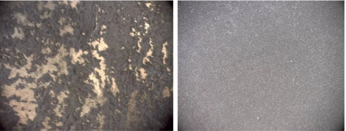
The metal film used bellow the absorber is used for the electroplating process and allows the plating current to circulate. The choice of the metal layer depends on the adherence on dielectric Spin-On-Glass film and on the compatibility with the electroplating process and finally on the low heat capacity. Experimental study shows the Chromium monolayer is not the best choice. The chromium has a good adherence with the SOG film but the tin deposit turns out to be not uniform presenting many defects. The chromium has not really compatibility with the tin electroplating and seems to be dissolved (Figure 7).
Figure 7 : Tin electroplating defects and in homogeneity in the tin deposit
chromium/copper
A second approach we have tested is to use a bi-layer Chromium/Copper because the copper has a good compatibility with the electroplating process and has a good adhesion with a chromium layer. Unfortunately, copper does not adhere on insulation film used. So it is necessary to use bi-layer materials. The chromium protected by a thin copper layer is not dissolved during the plating process. On the following picture (Figure 8), we can notice that the edges which are not protected by the copper are etched with lift-off of metal layers.
Figure 8 : Tin electroplating process on Chromium/Copper
Passivation on chromium and on chromium/copper
The idea is to investigate the tin electroplating on the Chromium and on the Chromium/Copper with an additional step of oxidation. Chromium and Chromium/copper samplers are immerged in hydrogen peroxide bath at 30% for 10 minutes. Then electroplating process is performed on this two samplers. The current density is 0.1 mA / mm2 in a solution composed of 1L H2O2 + 100 g K2Sn(OH)6 +
15 g KOH. The oxide layer protects the Chromium film and there is no dissolution of the film and we can see parts of tin deposit (Figure 9a). The oxidation of copper film seems to be removed during the plating process and there is a perfect tin deposit (Figure 9b).
Figure 9a) Tin deposit on Chromium oxidized Figure 9b) Tin deposit on Chromium/Copper oxidized
Titanium
Titanium and gold are used in the Silicon microcalorimeters developed in CEA. The idea is to try the electroplating process on a thin layer of titanium. Ti can be a good superconducting candidate which can replace the bi-layer Chromium/Copper. Moreover, titanium should adhere on SOG film. An experimental study is performed to conclude if Tin shows a good adhesion on Titanium. We use Ti foils (30 um of thickness) supplied by Goodfellow (purity 99,6%).A first cleaning step is carried out with hydrogen peroxide at 30% for 10 min. Then, the sample is dipped in the solution composed of 40 ml H20 + 14 mL nitric acid + 0,8 mL fluorhydrique acid for 10 min. After this cleaning step, we see that the edges of sample have been slightly etched. Finally, the sample is inserted in the
electroplating solution for 15 min. The electrolyze current is 0,1 mA / mm2, the temperature solution is 70 °C, the area of the sample is 225 mm2. To conclude, there is no adhesion of tin on the titanium layer (Figure 10a and 10b).
Figure 10a) Ti layer before electroplating tin and Figure 10b) Ti layer after electroplating tin
Gold
In the development of Si microcalorimeter, we use a bilayer Ti/Au. This couple of materials can be an interesting candidate to replace Chromium/Copper. We have tested the tin adhesion on gold pad. The adhesion of tin on gold is good and the tin deposit is uniform (Figure 11).
In the future, the use of Ti /Au can be the best choice. Ti has a good adhesion with SOG film and its superconductor behavior permits to have a low heat capacity at cryogenic temperature. Furthermore, there is a good adhesion between Ti and Au with an evaporation process and the tin electroplated deposit is very uniform.
Investigation
of
the
thermalization
performance
of
superconducting absorbers
Rationale
The absorber material of choice for X-Rays micro-calorimeters must have a small heat capacity to provide a measurable temperature rise after the absorption of a single photon, a high atomic number to provide high absorbing efficiency, and moreover, must have a fast and efficient thermalization of the deposited energy.
Normal metals would be ideal with respect to the last two requirements, however, their specific heat which is the sum of an electron contribution and a lattice contribution, according to the formula
3
AT T
C =
γ
+ withγ
and A, constant values of the material, is too large at low temperatures because of the electron contribution which is linear with temperature.Low gap semiconductors and Superconductors are considered as valuable candidates since they do not have an electronic term in their specific heat at low temperatures. What remains is the phonon contribution which is a function of the Debye Temperature of the material, at very low temperatures the specific heat can be calculated according to the formula
C ph = 1943.8 (T/TD) 3
[J/K·mol]
Both the groups in Palermo and in Paris are mostly interested in the use of superconductors. In the following. I discuss experimental tests that have been performed at the XACT facility of INAF-OAPA to investigate the thermalization performance of different candidate superconductor materials.
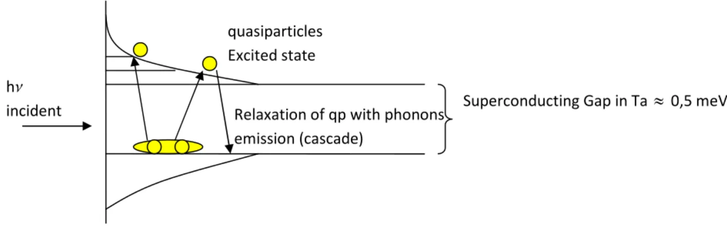
Energy thermalization in a superconductor absorber
The principle of a microcalorimeter depends on the conversion of the photon energy into a thermal phonon distribution in the superconducting absorber, producing a temperature rise, read out by a thermometer.
A soft X-ray Photon (E < 30 keV) interacts with matter mainly by photoelectric absorption effect. The absorption of a photon produces the extraction of an electron with a kinetic energy equal to the difference between the energy of the incoming photon and the binding energy of the ejected electron. This ejected electron by multiple collisions releases its energy to the crystal lattice in phonons. In a superconducting material, at temperature below the TC, the electrons are coupled in
Cooper pairs (at lower energy than 2 free electrons). The phonons created by the energy deposited by the absorbed photon, can either escape into the thermistor, decay enharmonically to a lower energy level or break Cooper pairs to form single electrons, called particles. These quasi-particles quickly recombine into Cooper pairs emitting a new phonon of the same energy (Figure 12).
Figure 12 : Thermalization process
Since the probability to break Cooper pairs is usually much larger than the probability of the other two mentioned processes (phonons escape or decay), the time needed to thermalize the absorbed energy into a phonon distribution in equilibrium can be long compared to the rise time (depending of the thermal impedance of the link absorber-thermometer and of the thermal capacity of the absorber (Figure 2)) of the signal pulse detected by the read-out electronics. In this case a significant fraction of the absorbed energy can still be trapped in the superconductor absorber and not detected. This effect known as quasiparticle energy trapping can affect the performances of a microcalorimeter with superconductor absorber.
Most of the superconducting materials do not provide great performances in the thermalization of the energy deposited. The excess of quasiparticles reach the lowest energy level and wait for recombination. Long recombination lifetimes contribute to delay the transfer of the energy trapped and the amount of undetected energy can degrade the spectral resolution of the detector. So it is necessary to have an estimate of the percentage of energy that is effectively thermalized.
A treatment is applied on the high purity tantalum foils which come from Alpha Aesar. Theses foils (25 µm of thickness) are cut and cleaned in a chemical mixture composed by fluorhydric acid, acetic acid and nitric acid. The chemical attack is well controlled and the removed layer is 2µm. A native oxide of 2nm appears on the surface of the samples. This oxide becomes instable and decays around 1500°C. We can assume that after an annealing process, the oxide has totally disappeared. It is important to outgas the material and homogenize the samples (suppression of cristal defects) by annealing at 2000°C during 2 minutes. The experimental system developed by the CSNSM permits to perform a cleaning process by Argon pulverization and annealing. It permits also to deposit metallic layers on the tantalum surface.
Last year, an experimental study has been performed on pure tantalum absorber (Ta/Au). The Superconducting Gap in Ta ≈ 0,5 meV hn
incident
quasiparticles Excited state
Relaxation of qp with phonons emission (cascade)
Tantalum (glued onto the gold) was built. The experimental results demonstrated that the thermalization of photons absorbed in tantalum is delayed by energy trapping in quasiparticles. With the Ta/Au prototype, two peaks were observed on the spectrum. In both peaks, we can see the Mn Kα and Mn Kβ lines (Figure 13) and the sharing of the counts among the two peaks corresponds to the area ratio between the tantalum spot and the gold drop. A calibration could be performed with the higher energy peak matched to photons absorbed, fully thermalized in gold and the shifted peak corresponding to photons absorbed in Tantalum. The energy shift is 1,8 keV. We conclude that 30% of the deposited energy is not thermalized in the tantalum due to the trapping by long living quasiparticles. The effective life time of quasiparticles is around 900 µs for pure tantalum with thermal treatment, which is important compared with anexpected rise time of 100 µs for a microcalorimeter .
One solution could be to force the quasiparticles recombination in Cooper pairs by the use of a thin layer of Aluminum or Nickel (on one side of the tantalum surface) to create a potential well for quasiparticles. The high density of quasiparticles achieved in this thin layer accelerates the thermalization process. The quasiparticle confinement in a small volume should promote the recombination process (Figure 14).
The goal of this new measurements campaign is to study the thermalization of the energy in an X-Ray microcalorimeter with Ta-Al/Au (Tantalum with one side thin Al layer glued on a gold drop).
Figure 14 : Principle and structure of Ta-Al/Au prototype
Ta Al 25µm 100nm Confinement of qp in the Al layer Recombination in Cooper pairs Incident photon : Cooper pairs breaking and quasiparticles (qp) formation
50µm x 50µm
Description and operation of the experimental setup
Measurements on the NTD Ge micro-calorimeters with various absorbers have been performed at temperatures between 50 and 100 mK. The following figure 15 illustrates the measurement bench including the cryostat, the pumping system, and the electronic rack.
Figure 15 : Measurement bench
The main principle of an Adiabatic Demagnetization Refrigerator is explained in annex 2. The description of the paramagnetic salt used is described in annex 1. The ADR cryostat of INAF-OAPA can reach a minimum temperature of 42 mK and can operate at 60 mK for several hours with an heat load onto the cold finger lower than 1 µW. The operation steps of the ADR are described in annex 3, the cryostat wiring and thermometry instrumentation are listed in annex 4.
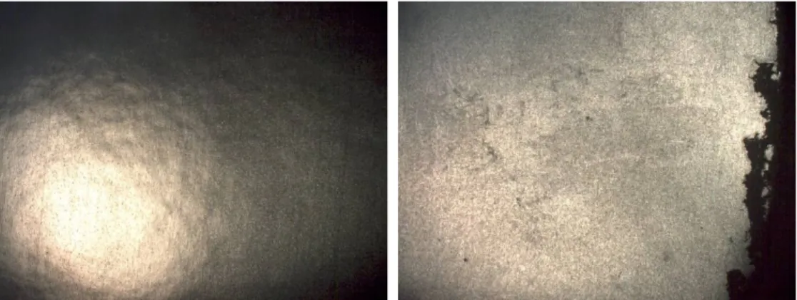
An iron 55 radioactive source has been used to illuminate the detectors. This source mounted outside the cryostat on a push-pull feedthrough emits 5.9 keV (Mn Kα) and 6.5 keV (Mn Kβ) X-ray photons. A shield screen can be inserted to protect the detectors from the X-ray illumination. Figure 16 shows a picture of the Iron source set-up. The microcalorimeters prototypes are illuminated uniformally without the use of a collimator.
Figure 16 : Picture of Fe55 source system.
Source displacement
Shield Screen displacement Entrance window of the
X-Ray photons
The detector box is protected from the radiation heat load by a set of three aluminized Mylar windows at the various temperature shields. The thickness of one layer of Mylar is 43 µm. The total transmission of the three windows is around 70% at 6 keV (Figure 17).
Figure 17 : Transmission curve of a MYLAR film 150 µm thick.
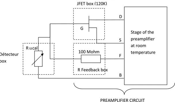
The electrical signals from the Ge thermometer are amplified by a first stage preamplifier mainly located at room temperature. The front-end circuit inside the cryostat includes 4 JFET transistors (4 channels) operating at 120 K located inside a box which is thermally attached to the LHe stage (Figures 18). Before cooling, the JFET circuits are checked (Annex 5). After this front-end JFET stage, there are 4 amplifiers at room temperature. So we have four electronic read out channels and it is possible to perform measurements on four microcalorimeter prototypes. The JFET circuit at 120K and the electronic at room temperature represent the preamplifier stage (Figure 19).
Diode thermometer
Kevlar suspension Heater
Figure 19 : Electrical diagram of the pre-amplifier circuit available for four channels. There are two possibilities to acquire and treat the measurements data (Figure 20).
Channel A :
A pulse shaping amplifier is connected to the multi-channel analyzer and to a computer using Maestro software. The pulse shaping amplifier filters the signal time curves and a multi-channel analyzer measures the peak amplitudes of the signal pulses and fill a histogram with number of counts versus the peak amplitude. Maestro is a software that provides a histogram display for pulse heights. This histogram when calibrated is converted into an energy spectrum.
Channel B :
The signal pulses are collected directly after the preamplifier circuit without using the shaping amplifier. The signal time curves are numerised without filtering, acquired and stored in an acquisition PC under Labview. Then an off line treatment with IDL can be performed on data measurements. More details on the acquisition system can be found in [4] and [5].
Figure 20 : Principle of measurements acquisition D S F B G 100 Mohm R µcal R Feedback box Stage of the preamplifier at room temperature Détecteur box JFET box (120K) PREAMPLIFIER CIRCUIT PREAMPLIFIER CIRCUIT R µcal JFET 120K PA 300K CRYOSTAT Post Ampl Shaping Amplifier Filterring Triggering Multichannel analyzer Pulse sensing PC Maestro software Display spectrum Numerisation of thermal curves versus time ADC Acquisition PC Labview Off line treatments and display (IDL) CHANNEL A CHANNEL B
Description of the detector prototypes to be tested
Samples of different superconductor materials, namely Tin, Ta, Ta+Al, Pb-Bi, Ta+Ni, WN+Si have been sent to Lawrence Livermore Berkeley laboratory (Berkeley, CA, USA) to build a set of NTD Ge microcalorimeters. Unfortunately, some of the detectors have not been built in time and we have not been able to set-up experiments to characterize all the desired samples. During my training period we have been able to set-up an experiment to test only one set of four microcalorimeters described below. A description of two more sets of microcalorimeters that are presently under design or construction is also given.
First set of microcalorimeters (built and available)
This set is composed of 4 detectors with the same kind of NTD Ge thermistor and different absorbers, namely Ta/Au, Ta-Al/Au (Al on one side), Sn/Au and Pb-Bi/Au. In order to be able to compare the thermalization performances of each superconductor material with a normal metal we have requested that a small piece of the superconductor was attached onto a thin layer of gold absorber 10 μm thick. The superconductor sample attached onto the gold is typically 50x50x25 μm3. Figure 21 shows a picture of this set of microcalorimeters. The small gold absorbers with square shape about 100 x 100 μm2 are clearly visible in the picture taken with the microscope.
Figure 21 : First set of microcalorimeters
A 50 um thick layer of tin (see the bottom part of figure 21) is mounted above the electrical connections of the detectors to the read-out electronics, to prevent X-ray photons to be absorbed in the wires. At 6 KeV, there is negligible transmission of X ray photons across this Tin foil (Figure 22).
Sn / Au PbBi / Au
Ta / Au
Figure 22 : Transmission curve for a layer of tin (50µm) The structure of the microcalorimeter with Ta-Al absorber is described in Figure 23.
Figure 23 : Ta-Al/Au sample
The thermal link between Ta and Au and between Au and the Ge thermistor is done by hand using an epoxy glue. No automatic process is used to build this kind of microcalorimeters. The detector is mechanically suspended by the aluminum wires that provide the bias current to the NTD Ge thermistor and output the signal. The aluminum wires are ultrasonically bonded to the Ge NTD and are attached with a drop of epoxy glue onto a saphire substrate that provides the thermal conductivity towards the cold bath. We have used NbTi wires with a diameter of 0,002 mm to connect the detectors to the read-out electronics.
Ta-Al (50 µm x 50 µm x 25 µm with an Al layer) 50 µm 25 µm Au 10 µm 150 µm 50 µm NTD Ge 50 µm 100 µm 100 µm Al layer about 0.1 µm deposited on Ta
Second set of microcalorimeters (currently being built and not yet available)
For this set of microcalorimeters, designed to test the following absorber materials, namely WN-Si/Au, Ta-Al/Au (Al on 2 sides), Ta-Ni/Au, and PbBi/Au, the structure of the detectors has been modified. A small piece of gold, likely 20x20x5 μm3 will be placed on top of the superconductor absorber. The gold volume and the heat capacitance are reduced with respect to the previous design. A collimator should be used in front of each microcalorimeter to equalize the counting rate on the gold and on the tested absorber.
Figure 24 and 25 describe the structure of the WN-Si/Au on a silicon bulk and of the Ta-Al/Au detectors. The presently available samples built on a Si bulk 700 microns thick are difficult to build ontop of a much smaller size NTD Ge sensor. To reduce the thickness of Si on these samples, either by mechanical polishing or chemical etching, could damage them. The LETI laboratory in grenoble will be able to supply new samples with a thinner layer of silicon bulk.
Figure 24 : Structure of Prototypes WN/Au sur Si
Gold drop or pad (20µm x 20µm x 5µm) Ta aluminised on two sides 500 µm 2 µm NTD 500 µm 500 µm Goutte ou pad en or (1µm x 1µm x 1µm) Gold drop or pad (20µm x 20µm x 5µm) WN 500 µm 2 µm Bulk silicon 700 µm 150 µm 50 µm 50 µm NTD Ge
Given the difficulty of the American laboratory in manufacturing very small pieces of gold, one solution is that the CEA could provide the absorber with a thin layer of gold deposited (about 0.4 μm thick on the fill surface). These absorbers can then be mounted on the NTD Ge thermistors in an easier way so that we can test the new set of detectors in the near future at the XACT facility in Palermo.
Third set of microcalorimeters (currently being built and not yet available)
A third set of microcalorimeters, designed to test the following absorber materials, namely pure Tin, Tin+Sb, Tin+impurities (Fe and Co), and PbBi, has also already been built and will be tested in the future. In order to take full advantage of the measurements of this set of detectors it would be better to first optimize the experimental apparatus to reduce the significant electromagnetic ambient noise that we have experienced during the measurements described below.
Experimental results and Discussion
We have tried to collect some spectrum on the 4 absorber prototypes during the few hours when the ambient noise was lower. The spectrum for the Pb-Bi and the pure Tantalum has not been performed due to the important level of ambient noise. Only the Ta-Al/Au and Sn/Au prototypes have been measured.
Figure 26 shows pictures of the set of four tested microcalorimeters mounted inside the detector box of the cryostat.
Figure 26 : On the right - tested microcalorimeters mounted inside the detector box and on the left - zoom of the absorbers area
Ta-Al/Au
For our measurements, a thin layer of aluminum has been deposited at the Ta/Au absorber. Gold is a noble metal, has not a superconducting behavior at low temperature and has a good heat conduction. We expect that the thermalization properties are excellent and that 100% of the energy of the photons absorbed in gold is fastly thermalized. The fact that we add a layer of aluminum should improve the thermalization process in the Ta-Al absorber and we would like to compare with the Ta/Au absorber.
To perform Ta-Al/Au measurements, we acquired the data from channel A (Figure 18). These measurements are filtered by the pulse shaping amplifier and the multichannel analyzer connected to the Maestro PC permits to have a spectrum. The figure 27 shows the measured spectrum for the Ta-Al/Au at 60mK as displayed directly by the Maestro program. An energy scale has been added on the following spectrum, by assuming that the maximum of the spectrum corresponds to the 6 keV line, but it is not the best solution. We do not see two peaks, one of which could be attributed to gold, so, in fact, it is not possible to calibrate the spectrum in energy.
Figure 27 : Plot of spectrum for Ta-Al/Au (data extracted from Maestro program)
We have smoothed the measurements on Ta-Al/Au using a running average on 16 points to improve the readability (Figure 28).
Ta-Al/Au 0 50 100 150 200 250 300 500 600 700 800 900 1000 1100 1200 1300 channels c o u n ts
Figure 28 : Spectrum for Ta-Al/Au (smoothing treatments)
We assume that the mean value of the spectrum corresponds to the 6 keV line. And in this way we can convert the channel axis in energy scale.
The mean value can be deduce from the measurement by using this following formula :
Where picorresponds to the number of counts in the bin xi The mean value is around 910 channels which correspond to 6 keV.
The standard deviation is given by :
The standard deviation is around 110 channels. The Full Width at Half Maximum (FWHM) is given by :
The FWHM calculated is 259 channels, so around 1,7 keV. We do not see a distinct spectrum for gold and for tantalum, but a large spectrum with 1,7 keV of FWHM. In the case of the pure tantalum data presented in figure 13, the two peaks are separated by 2 keV and would be clearly separated even with a spectral resolution as large as the 1,7 keV FWHM of this new measurements. Then, we can conclude that the aluminum layer added on tantalum improve the recombination of quasiparticles and the thermalization process.
The second idea was to collect some pulses on channel B (signals out without shaping) (Figure 20) and we have tried to visualize a spectrum for the Ta-Al/Au with data treatments on IDL. It was a first approach to improve the measurement quality.
The following figures show a pulse collected lost in the noise (Figure 29) and a smoothed pulse (Figure 30). The Figure 31 shows the average pulse for the Ta-Al/Au absorbers.
The base line is very noisy (Figure 30) with a lot of low frequency noise. The pulse signal starts at 100ms and the base line is given by the data between 0 and 100ms on the temporal curve.
Example of pulse collected before amplifier shaping -30 -20 -10 0 10 20 30 40 0 50 100 150 200 250 300 Time [ms] C o u n ts
Figure 29 : Example of pulse collected
Example of smoothing pulse
-100 -50 0 50 100 150 200 250 300 350 400 450 500 0 50 100 150 200 250 300 Time [ms] V o lt a g e [ m V ]
Figure 31 : Averaged pulse versus time
We tried to filter the data with an IDL treatment. It was a first approach to see if the readability of the pulses data could be improved. The spectrum with a Wiener filter is represented on the figure 32.
Study of the time curves :
The last idea is to derive the decay and rise time of each pulse and evaluate if we see two populations corresponding to the detection of photons in gold and tantalum.
Most of the pulses are clustered around a rise time of 400 µs and a decay time of 9 ms (Figure 33). And we do not see any structure corresponding to two different populations. This was not the case with the Ta/Au microcalorimeter prototypes [6].
Sn/Au
The following figure shows the spectrum for the Sn/Au. The Sn/Au measurements have been performed at 65 mK (Figure 34) and have been acquired with the channel A (Figure 20). The Sn is a good thermalizer and it is possible to compare the Ta-Al/Au and Sn/Au spectrums (Figure 35).
Sn/Au 0 10 20 30 40 50 60 70 80 90 100 110 120 130 140 500 600 700 800 900 1000 1100 1200 1300 Channels C o u n ts
Figure 34 : Spectrum for Sn/Au (smoothing treatments)
The mean is around 921 channels which correspond to 6 keV. The standard deviation is 56 channels and the FWHM is next to 130 channels which corresponds to 0,86 keV.
Spectrum Ta-Al/Au and Sn/Au
0 25 50 75 100 125 150 175 200 225 250 275 300 500 600 700 800 900 1000 1100 1200 1300 C o u n ts T a-A l/ A u 0 15 30 45 60 75 90 105 120 135 C o u n ts S n / A u Ta-Al/Au Sn/Au
demonstrated by the fact that we could not take any data with the two other microcalorimeter prototypes (Ta/Au and PbBi/Au) mounted in the cryostat during this measurement campaign.
Discussion and prospective
We can conclude that the thermalization process is improved by adding the Aluminum layer on Tantalum. However, the very noisy pulses and poor energy resolution associated forces us to be prudent in the conclusions. Further analysis should be performed to verify if more accurate results can be derived from the available pulses, while a new measurement program should be scheduled after the cryostat wiring has been revised.
We can precise that some measurements have been performed in the same time at the IAS “Institut d’Astrophysique Spatiale” with a Pu238 source which show good results with a FWHM at or lower than 12 keV for alphas of the Pu source (Figure 35).
Figure 35 : Spectrum for Ta-Al/Au with Alphas of Plutonium
During the measurements in Palermo we experienced a very strong electromagnetic ambient noise which made it very difficult to distinguish the photon pulses above the noise on the oscilloscope. Furthermore, the detected rate of photons was very low (less than 1 cts/s), this is partially due to a reduced radioactivity of the Iron 55 source (more than 5 years old) and due to a non ideal mounting of the source. Only few hours during one of the nights of the measurement program the ambient noise was significantly lower and allowed us to detect a few photons.
Given the strong ambient noise that was experienced we have decided to re-analyze the wiring of the cryostat and in particular the wiring between J-FET and detector boxes that presently use un-shielded wires. Furthermore, the heater in the JFET box seems also to be a potential source of noise incoming into the J-FET box. It will be interesting to add a heater by optical fiber for example.
Moreover, the post-amplifier and pulse-shaping amplifier have been provided to INAF-OAPA by a collaborating research group in USA and there is very poor if any documentation that can be used to
optimize the performances of such devices. It is a real problem to well understand without schematic, gain, level of noise etc…
Conclusion
This training period permits to study the Germanium microcalorimeters technology and to compare with the Silicon microcalorimeters technology. Tin electroplating deposition and experimental tests allow us to optimize the standard process for the Ge microcalorimeter.
The second part of training period permits to conclude that the Ta-Al/Au absorber remains a candidate for the Silicon microcalorimeter as it has a better thermalization process than the Ta/Au absorber. Unfortunately, due to unexpected Electromagnetic Noise in the experimental set-up the measurement campaign conducted during my training period in Palermo was not fully successful, and new measurements will be performed after the ADR cryostat wiring will be revised.
References
[1] P. Verhoeven, “Photon Counting Low Temperature Detectors for Visible to Gamma Ray Astrophysics”, J. of Low Temp. Phys, vol 151, May 2008.
[2] Shklovskii, Efross, “Electronic Properties of Doped Semiconductors”, Springer-Verlag, 1984 [3] A. Aliane, “Design and fabrication process of silicon micro-calorimeters on simple SOI technology for X-ray spectroimagery”,Nuclear Inst. and Methods in Physics Research, 2008
[4] E.Silver, “An NTD germanium-based microcalorimeter with 3.1 eV energy resolution at 6 keV”, Nuclear Instruments and Methods in Physics Research, 2005
[5] E.Silver, “High resolution spectroscopy using germanium microcalorimeters”, X-Ray and Gamma Ray Instrumentation for Astronomy and Atomic Physics, 1989
[6] E. Perinati, “Experimental evidence of an incomplete thermalization of the energy in an x-ray microcalorimeter with a Ta/Au absorber”, Review of scientific instruments, 2008
Annex 1 : Paramagnetic salt used in the ADR of the INAF-OAPA
The paramagnetic salt used in the ADR of the INAF-OAPA is the Ferric Ammonium Sulphate dodecahydrate (FeNH4(SO4)2 12H20), provided by Sigma-Aldrich with a purity of 99.99%.
The paramagnetic salt must be confined in an insulated vessel to prevent the loss of the crystallized water molecules and must be in a good thermal contact with the cold finger which is a copper rod. The thin walls salt container is made of stainless steel which has a good strength and a good resistance to salt chemical etching. Gold wires (120 mm long and 0,25 mm diameter) are drowned inside the crystal container to have a good thermal link between the salt and the cold finger (Figure 36). The salt container is suspended by Kevlar wires to minimize the heat load from the helium bath.
Figure 36 : Salt Pill container
1) 3) 4 ) 5) 7) 2) 2) 2) 2) 8) 8) 6) 9) 10) 11) Legend
1) Cu rod (cold finger)
2) TIG welding (caps and cylinder) 3) Silver soldering (cap and Cu rod) 4) Gold soldering (wires bundle and Cu
rod) 5) Epoxy
6) Container (stainless steel INOX 304) 7) Gold wires bundle
8) Screw eyes
9) Vacuum seal screw 10) Upper cap 11) Lower cap ___________________________________ Material Weight [g] Stainless Steel 32.35 Gold 14.76 Copper 24.64 FAA 124.62
Annex 2 : Principles of an adiabatic demagnetization refrigerator
One method to obtain cryogenic temperature below 1K is the use of the adiabatic demagnetization refrigerator (ADR). The following pictures (Figure 37) show the cryostat used for the absorbers measurements.
Figure 37 : overview of the cryostat and associated zoom
The main components of an ADR are: a magnet, a paramagnetic salt pill such as Ferric Ammonium Alum dodecahydrate (FeNH4(SO4)2 12H2O), a thermal heat sink between the salt and a cold bath and
a magnetic shield (Figure 38).
Figure 38 : Main parts of an ADR
Paramagnetic salt pill + thermal bus Superconducting magnet
Cold bath Detector box Thermal contact Magnetic shield
A paramagnetic material is composed of magnetic moments which mutually interact. At the temperature of pumped liquid helium, the interaction energy between magnetic moments is negligible with respect to the thermal energy of the molecules. The molecular thermal energy is high and therefore there is a random orientation of magnetic moments. The entropy associated to the magnetic moment disorder is large compared to all the other entropy contribution of the system (lattice, conduction electrons). When the temperature decreases, the contribution of the thermal energy becomes lower and the interaction energy between magnetic moments will become similar to the thermal energy.
When an external magnetic field is applied, magnetic moments start to align. The larger is the magnetic field intensity, the larger is the number of aligned magnetic moments. This magnetic moments alignment produces a decrease of the total entropy. The transformation is exothermal, because magnetic moments go into lower energy states releasing the excess energy, and a thermal link between the salt and the thermal bath permits to evacuate the heat produced during the magnetization.
If the paramagnetic material is now thermally isolated by opening an heat switch and the external magnetic field is decreased, the magnetic moments of the salt turn back to their random orientation. This transformation is endo-thermal. The system is isolated thermally, the moments will pick up thermal energy and the material temperature will decrease until thermal energy becomes equal to the interaction energy between magnetic moments.
When the sample is demagnetized completely, the entropy of the spin system comes from the vibrations of the lattice. At this cryogenic temperature, the entropy due to the vibration of the lattice is low. During the adiabatic demagnetization process, the total entropy of the salt remains constant. The increase of entropy of the magnetic moments, due to increasing random orientation, is compensated by a decrease of the entropy of the lattice which cools down.
Annex 3 : Structure and operation of an adiabatic demagnetization
refrigerator
Cryostat vacuum pumping system
A pumping system consisting of a ceramic bearing turbo-molecular pump Varian model Turbo-V 300HT (nominal speed 300 l/s) with a membrane back-up pump is used to vacuum the ADR cryostat. The vacuum level must be around 10-4 mbar before the liquid Nitrogen and liquid Helium can be poured inside their vessels for cooling. If the cryostat has been open to air for a long time to mount detectors and operate on the wiring, it can take more than one day to reach an adequate vacuum level.
Two mechanical rotary pumps are used to vacuum the vapour above the liquid Nitrogen and Helium in order to reduce their equilibrium temperatures. Figure 39 shows a picture of the control panel of this pumping system. The nitrogen and helium lines are composed of a pressure gauge [0 – 800 Torr], a block valve for raw pumping regulation, a needle valve for fine regulation and a safety valve regulated to 1.5 bar. The helium pumping line has a second and more accurate pressure gauge operating in the range 0-50 Torr.
Figure 39 : Control panel of the pumping system
Pre-cooling the Dewar
The cryostat is composed of three main parts: the liquid nitrogen tank (77 K), the liquid helium tank (4 K), and finally the magnet cavity (Figure 40).
Figure 40 : Structure of the cryostat
The cooling of the cryostat from ambient temperature to pumped LHe temperature takes about one day. With the pump system running, we start pre-cooling by filling the cryostat with liquid nitrogen in the LHe and in the LN2 vessels. After a few hours the temperature on the cold plate is around 77 K. When the two vessels have reached 77 K, we can start cooling with liquid helium. Before transferring the LHe, the residual LN2 in the LHe tank must be fully removed. The first helium transfer takes about 1/2 hour and the cold plate of the cryostat reaches the LHe temperature after a few hours. Pumping on the liquid He vessel to reach the minimum temperature of about 1.8 K takes about 4 hours.
Adiabatic demagnetization cooling
Figure 41 shows the entropy diagram for 125 g of FAA paramagnetic salt. The different curves represent different values of the external magnetic field intensity from 0 to 3,5 Tesla.
Figure 41 : Entropy diagram of 125 g of FAA paramagnetic salt
Isothermal magnetization
Adiabatic démagnetization
The 1-2 step is the application of the external magnetic field with the salt container in thermal contact with the cold bath at the temperature of the pumped liquid helium. The energy of interaction of the magnetic moments of the ions with the magnetic field decreases and the moments are oriented along the field axis. The 2-3 step is the removal of the external magnetic field with the salt pill thermally isolated. The thermal contact between the cold finger and the bath can be opened or closed using a mechanical switch. The temperature decreases until the thermal energy of the ions becomes equal to the interaction energy between the magnetic moments themselves. The minimum temperature that a paramagnetic salt can reach after the demagnetization step depends on the interaction energy of the paramagnetic ions and will be lower for salts with smaller magnetic moments and larger mutual distance.
Isothermal magnetization. The thermal link between the bath and the salt pill is closed. A progressive ramp of current is applied on the superconducting magnet (Figure 42). The duration of this step lasts several hours. The speed of the current can be modified and is usually around 1-2 mA/s. When the magnet current reaches the maximum value (5 A), the pill salt is thermally disconnected from the thermal bath and the process of adiabatic demagnetization can start. The disorganization of the magnetic moments creates a decrease of the temperature. The minimal temperature is around 50 mK.
Figure 42 : magnetization step
The system control uses a Labview software to control the current of the superconducting magnet and to maintain a constant temperature in the paramagnetic salt.
magnetic field B decreases too with a hysteresis effect (Figure 43). When H is equal to 0, there is again a magnetic field Br called “remanent field”.
Figure 43 : B = f(H) for a soft magnetic alloy
A ferromagnetic material shield permits to channel the magnetic field lines inside the material. But after magnetization of this shield, the material can keep a part of magnetization. So this solution can be a problem in the diminution of the magnetic field. A Hyperco 50A shield with high magnetic permeability (µr = 3520) is installed around the magnet to reduce the residual magnetic field, in fact this residual magnetic field can have an effect on the detector measurements. This material contains 50% of cobalt, 2% of Vanadium, 0.01 % of carbon, 0.05 % of manganese, 0.05 % of silicon and is a soft magnetic alloy. To delete this remaining field, one solution can be to use a superconducting shield around the ferromagnetic field. When a material makes the transition from the normal to superconducting state, it actively excludes magnetic fields from its interior, this is called the Meissner effect. The Meissner effect allows to reduce totally the remanent field. The magnetic shield and the magnet are attached to a gold coated copper plate providing a good thermal link with the liquid helium bath.
A magnetic simulation of the residual magnetic at the detector place has been realized on FEEM (Finite Element Method Magnetics) (Figure 44) :
Figure 44 : Simulation of magnetic field (2D) on FEEM software
A magnetic simulation (2D) gives a residual magnetic field of 230 mT at the detector box at maximum field in the solenoid (3 T). If this residual field should be a problem during the magnetization phase, the option of building a superconducting shield of the detector box can be considered.
Coercitive excitation < 100 A.m-1 High permeability.
Annex 4 : Cryostat wiring and thermometry instrumentation
Wiring :
Thermometry instrumentation :
The thermometry instrumentation is composed of :
• RuO2 (Ruthénium oxyde) located on the Liquid helium plate. • Diode (DT-670) located in the electronic box.
• Germanium Resistance (GR-200A-30 Lakeshore - range = 0,05 à 1,15K) placed in the detector box
• Germanium Resistance (Ge 28945) placed on the liquid helium shield Control of the instrumentation before pumping at room temperature (Figure 45):
Thermometers Measurement RuO2 1,01 Kohm Diode 0,545 V 16 coaxial wires Lakeshore Type SS L = 87 cm
2 brass wires L= 43 cm Diameter = 2 mm
Magnet Current supply
+ 2 brass wires L= 31 cm Diameter = 1.5 mm Thermometers
4 NbTi wires L= 20 cm Diameter = 0,05 mm Resistance bridge + 4 Lakeshore cryocables L = 80 cm 16 coaxial wires Lakeshore Type SS L = 87 cm Détecteur box 8 Nb-Ti wires L = 10 cm Pre-Amplifier box JFET box Diameter = 0,02mm 8 Nb-Ti wires
Annex 5 : Check of the JFET electrical circuit
The following schematic describes the check circuit of JFET (Figure 46) .
Figure 46 : JFET and continuity wiring check circuit
For each channel, we measure the current IDS to check that the transistor and the instrumentation cable works well. At first, R µcal is connected (RF is not connected) and we change the VGS voltage by varying the variable resistor and we measure the current IDS. Then, we disconnect the R µcal and we connect the feedback resistor RF using the same configuration to measure IDS. Thanks to this configuration, we check the wiring continuity and the JFET operation prior to the cooling. After checking, the feedback resistor will be reconnected to the preamplifier at room stage for proper operation (Figure 47).
Channel IDS max
1 RF 440uA 1 RB 446uA 2 RF 443uA 2 RB 444uA 3 RF 442uA 3 RB 440uA 4 RF 444uA 4 RB 446uA
Figure 47 : Maximum current IDS measurement for each channel
The final check is the measurement of the heater for the JFET, the measured value for the heater in the JFET box is 580ohm.
I 22K D G S RF 100K 150K Variable resistor + 10 V - 10 V JFET BOX IDS VGS R µµµcal µ
Annex 6 : Code for the Spectrum plot with IDL
pro read_spe
dummy='bye'
cal=fltarr(2);;création d'un vecteur à 2 élements float
data=transpose(intarr(2048)) ;création d'une colonne avec 1024 données
openr, 1, 'D:\cryostato\SPECTRUM JUIN\Ch2_20090619_01.spe' ; ouverture d'un fichier avec le chemin du dossier à ouvrir
for i=1, 12 do begin ;boucle pour lire et passer les 12 premières lignes du fichier de données
readf, 1, dummy
endfor ; la lecture se fait séquentiellement jusqu'à la ligne 12
readf, 1, data ; lecture des data
print, data ; print des data
for i=1, 8 do begin ; lecture séquentielle des lignes du programme
readf, 1, dummy
endfor
readf, 1, cal ; lecture des 2 paramètres du modèle
close, 1
print, cal[0], cal[1]
;print, data
help, data
ch= indgen(2048) ;generation d'un index croissant de 0 à 1023
Energy=cal[0]+cal[1]*ch
coor=where(data eq max(data))
print, coor
a=cal[0]+cal[1]*coor
print, a
Plot,energy, data, title='Channel 2 Ta-Al/Au T=60mK', $
/YLOG, yrange=[1,100], xrange=[3000,8000], background ='FFFFFF'X, color= '000000'x, xtitle='Energy [keV]', ytitle='Counts'