HAL Id: hal-02901047
https://hal.archives-ouvertes.fr/hal-02901047
Submitted on 20 Jul 2020
HAL is a multi-disciplinary open access archive for the deposit and dissemination of sci-entific research documents, whether they are pub-lished or not. The documents may come from teaching and research institutions in France or abroad, or from public or private research centers.
L’archive ouverte pluridisciplinaire HAL, est destinée au dépôt et à la diffusion de documents scientifiques de niveau recherche, publiés ou non, émanant des établissements d’enseignement et de recherche français ou étrangers, des laboratoires publics ou privés.
triple-junction solar cell metallization
Clément Laucher, Gwenaelle Hamon, Artur Turala, Maité Volatier, Maxime
Darnon, Vincent Aimez, Abdelatif Jaouad
To cite this version:
Clément Laucher, Gwenaelle Hamon, Artur Turala, Maité Volatier, Maxime Darnon, et al.. Self-powered light-induced plating for III-V/Ge triple-junction solar cell metallization. Energy Science & Engineering, Wiley, 2020, 8, pp.3672-3681. �10.1002/ese3.774�. �hal-02901047�
Energy Sci Eng. 2020;00:1–10. wileyonlinelibrary.com/journal/ese3
|
11
|
INTRODUCTION
Metal deposition for the front emitter contact of III-V/Ge triple-junction solar cells is a critical step in solar cell fab-rication for concentrated photovoltaics (CPV) application. Indeed, to operate under high concentration, the front con-tact metallization needs to be thick, usually around 5 μm1,2
in order to collect high current density solar concentrations of few hundred suns. In addition, to have the lowest series resistance in the solar cell, this deposited metal needs to have a good quality that ensures a very low resistivity. Finally, the ohmic contact layer deposited before the thick emitter
contact must provide a very low specific contact resistance. Hence, the process to deposit the front emitter contact is very complex and expensive. It is therefore important to develop a deposition process which is fast and easy to implement in industry and that provides low series resistance as well as low contact resistance. Nowadays, evaporation3 and
electro-plating2 are the most common methods to deposit the front
emitter contact. Electroplating is more cost-effective than evaporation; however, it requires connecting both the front side and an anode to a power supply. In usual process, the deposition of a seed layer by e-beam evaporation on the full wafer is first required. Then, a photolithographic step defines
Received: 20 January 2020
|
Revised: 9 May 2020|
Accepted: 1 June 2020 DOI: 10.1002/ese3.774R E S E A R C H A R T I C L E
Self-powered light-induced plating for III-V/Ge triple-junction
solar cell metallization
Clément Laucher
|
Gwenaëlle Hamon
|
Artur Turala
|
Maïté Volatier
|
Maxime Darnon
|
Vincent Aimez
|
Abdelatif Jaouad
This is an open access article under the terms of the Creative Commons Attribution License, which permits use, distribution and reproduction in any medium, provided the original work is properly cited.
© 2020 The Authors. Energy Science & Engineering published by the Society of Chemical Industry and John Wiley & Sons Ltd. Laboratoire Nanotechnologies et
Nanosystèmes, LN2, CNRS, 3IT (Institut Interdisciplinaire d’Innovations Technologiques), Université de Sherbrooke, Sherbrooke, QC, Canada
Correspondence
Abdelatif Jaouad, Laboratoire
Nanotechnologies et Nanosystèmes, LN2, CNRS, 3IT (Institut Interdisciplinaire d’Innovations Technologiques), Université de Sherbrooke, 3000, Boulevard de l’université, Sherbrooke, QC, Canada. Email: [email protected]
Funding information
Unité Mixte Internationale UMI, Grant/ Award Number: 3463; Université de Sherbrooke (UdeS); Université de Lyon; ECL; INSA Lyon; CPE; Université Grenoble Alpes (UGA); NSERC; CNRS; ANR, Grant/Award Number: ANR-17-ERC2-0035-01; STACE; Mitacs, Grant/ Award Number: IT10319
Abstract
We present a new process to deposit thick front emitter contact on multijunction solar cells using a self-powered light-induced plating (SP-LIP). This electrochemical deposition method is based on the use of the light-induced polarization of the cell to drive the plating current instead of the use of an external power supply as for standard electroplating. The electrical characterization of the process is performed by current and potential measurements at various light intensities and enables the deposition of thick layers of various metals (Ag, Ni, and Au) on triple-junction solar cells with a precise control of the metal thickness. The potential of SP-LIP for the deposition of an ohmic contact layer directly on the solar cell front side without any seed layer is also demonstrated. A triple-junction solar cell fabricated with both ohmic and thick metal front contact deposited only by an electrochemical method is reported.
K E Y W O R D S
concentrated photovoltaics, electrochemical characterization, electrochemical metal deposition, front emitter contact triple-junction solar cell, light-induced plating
the footprint of the grid pattern where the thick metal is de-posited by electroplating. After deposition, a final etching step removes the residual seed layer from the nonpatterned surface.
Light-induced plating (LIP) is a deposition process similar to electroplating, in which the power supply is the solar cell itself under illumination.4 Most of the time, the LIP process is
used with an external power supply such as a voltage source (Figure 1A). In fact, LIP is an electroplating method using a light source to assist the deposition process that avoids the need for an electrical contact between the seed layer and the power supply. This process has already been studied for the silicon solar cell fabrication5-9 and has been demonstrated at the
indus-trial scale for silver plating.10 Moreover, compared to classical
deposition processes used for silicon solar cells, light-induced plated cells have a better fill factor11 and reduced series
resis-tance losses, proving the high quality of the deposited material. Yet, most of the LIP processes reported on silicon solar cells use a setup with an external power supply connected between the rear side of the cell and the anode.5,8,9,12-14 Few studies on
silicon solar cells have also investigated methods to deposit front contact without any other external power supply.15,16
In this study, we propose a LIP process for the deposi-tion of thick emitter contact of CPV solar cell. This process called self-powered light-induced plating (SP-LIP) is similar to a LIP deposition method but without using any external power supply (Figure 1B). In fact, in this kind of setup, the illuminated solar cell is the only power supply in the system. SP-LIP is a simple process that could be attractive to reduce the fabrication cost of thick front contact of CPV solar cells. Indeed, SP-LIP is similar to electroplating and only needs to connect the rear side of the cell to the anode. Moreover, as the solar cell is only connected on the rear side, there is no need for a seed layer on the front side of the cell.13,14,16 So,
using SP-LIP, we could deposit the front contact using elec-trochemical methods only and avoid evaporation and etching steps, resulting in a large gain of time.
In this article, we present electrochemical characteriza-tions of the solar cell during SP-LIP experiments. Thanks to those, we manage to have an accurate control on the depos-ited thickness. Then, we present a novel method to deposit ohmic contact and thick front contact layer on triple-junction solar cells by SP-LIP. We demonstrate then the first func-tional triple-junction solar cell with front contact metals fully deposited by SP-LIP and we characterize its performance under 1 sun and concentrated light illumination.
2
|
SELF-POWERED LIP
CHARACTERIZATION
All the characterization experiments presented in the follow-ing section were performed usfollow-ing the silver-platfollow-ing solution. Those experiments are aimed to calibrate and control the deposition process.
The solar cell used is a standard InGaP/InGaAs/Ge tri-ple-junction solar cell grown by MOCVD on a Ge sub-strate. Solar cell dimensions were 7.648*6.648 mm2 with a
front emitter contact pattern with 56 fingers with a pitch of 120 μm. GaAs contact layer of the solar cell was etched using a NH4OH:H2O2:H20 solution in a self-aligned process. The
backside base contact was metalized with evaporated Ni/Au. This contact was bonded with silver paste to a conductive holder to ensure mechanical and electrical contact between the holder and the measurement instruments. The edges of the cell were protected using an insulator resist to avoid metal deposition during the SP-LIP on solar cells side.
A 500 W halogen lamp was used to illuminate the cell. The lamp emits a broad range of wavelengths between 300 and 2500 nm, which generates current in all three junctions of the cell. It was illuminated through a thin layer chromatogra-phy (TLC) tank of 0.88 L with flat glass sides containing the plating solution. The plating and electrochemical characteri-zations were performed at room temperature.
FIGURE 1 (A) Setup for LIP deposition used by Mette et al7. (B) Setup for self-powered LIP (SP-LIP) deposition, anode is generally Ag, Ni, or Pt electrodes depending on the deposited metal
|
3LAUCHER EtAL.
For Ag SP-LIP development and electrochemical charac-terization, we used samples with a thin (150 nm) Ni/Ge/Ni/ Au seed layer patterned by lift-off with 8-μm-wide fingers. A second lithography step is performed in a thick photoresist (NR4-8000P) with 5-μm-wide trenches aligned on the 8-μm-wide fingers defined in the seed layer. Technisol Ag 2460 RTU silver-plating solution was used for this study with a concentration of 20 g/L.
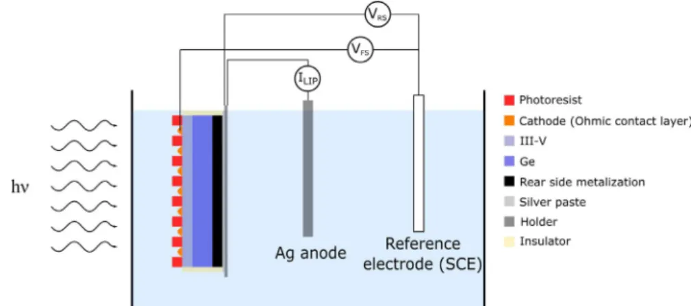
Characterization experiments were carried out using the setup shown in Figure 2, and the different voltages and cur-rents were measured with high precision multimeters. A sil-ver anode and a saturated calomel electrode (SCE) were used as counter electrode and reference electrode, respectively, while the solar cell front side acted as the working electrode. Illumination intensity was calibrated using a similar solar cell with the same grid pattern on the front side as the plated cell but with a thick evaporated Au front electrode. Solar cell short-circuit current is measured at different illumination in-tensities of the lamp. This current is then compared to the short-circuit current measured with a 1 sun solar simulator to evaluate the equivalent light intensity in suns. Note that the spectrum of the halogen lamp differs from the solar spec-trum, so that the real illumination is not precisely identical to sunlight illumination. As the cell has a photoresist coat-ing on the front side and sometimes the GaAs contact layer, the current generated by the plated cell compared to the cell active area is always less than for the reference cell. Before each SP-LIP experiment, light intensity was calibrated using this method. The good reproducibility of our results confirms the validation of this calibration method. Note that the light spot was adjusted to 4 cm2 in order to prevent heating up
the plating solution during the process. Only 1℃ temperature increase was observed after 15 minutes at lamp full power.
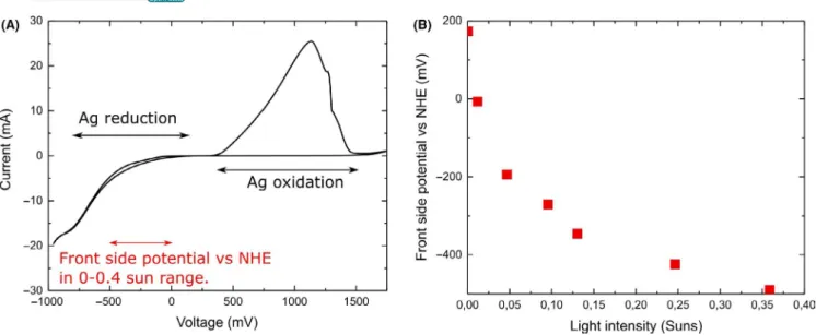
First, the silver-plating solution was characterized using cyclic voltammetry to know the voltage range where silver is deposited. As shown in Figure 3A, the reduction of the silver (ie, metal deposition) occurs when the current is negative. Therefore, the silver deposition occurs in a voltage range be-tween 0 mV and – 800 mV with respect to the NHE (normal
hydrogen electrode). We also measured the potential between the cathode (the front side grid of our cell) and a SCE (satu-rated calomel electrode) reference electrode at different illu-minations using the setup shown in Figure 2. Using this setup, we were also able to measure different electrical parameters during the SP-LIP process. The first parameter that needed to be identified was the range of light intensity that polarizes the solar cell at an operation point that corresponds to an electro-deposition regime. The results shown in Figure 3B indicate that the potential of the front side of the cell is between 0 and −450 mV at an illumination of 0 to 0.38 sun. This shows that silver deposition occurs in an illumination range of 0 to 0.38 sun (at least). This range was used during our experiments to insure operation in Ag deposition regime.
The SP-LIP current density plotted against light intensity is shown in Figure 4A, where the LIP current density is cal-culated considering the LIP current and the exposed metallic surface where the silver is deposited. For our triple-junction solar cells, the SP-LIP current density as a function of light intensity is linear in the measured range. It is worth mention-ing that for silicon solar cells, SP-LIP current density satu-rates around the light intensity of 0.3 sun.6 This difference is
attributed to the Voc difference between cells. Multijunction
solar cells have a much higher Voc (>2 V at one sun)
com-pared to silicon solar cells (<750 mV at one sun) which al-lows higher current increase before the cell starts to limit the current.
In order to assess the impact of the solar cell voltage, we measured both front and rear sides’ potentials as a function of light intensity to define the solar cell voltage at different intensities (Figure 4B). The solar cell voltage as a function of light intensity has a logarithmic behavior, which has also been observed for silicon solar cells.7 For our operating
con-ditions, the multijunction solar cell voltage (corresponding to
VRS-VFS) remains between 0.2 V and 1 V which is below the
multijunction solar cell Voc, while it would exceed a silicon
solar cell Voc (typically below 0.75 V at 1 sun). Therefore, the
multijunction solar cell operates as a current source while a silicon solar cell would enter a voltage limited regime.
FIGURE 2 Electrochemical
characterization setup used with the silver solution. ILIP is the current measured between the rear side of the cell and the Ag anode. VFS is the potential of the front side and VRS is the potential of the rear side. The solar cell voltage is defined as VRS-VFS
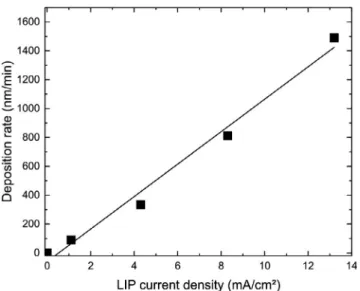
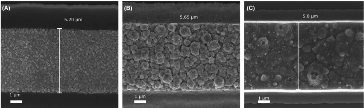
The metal deposition rate plotted vs SP-LIP current density curve is visible on Figure 5. As expected, the values follow a clear linear tendency. The deposition rate is also directly correlated to the silver morphology. Figure 6 shows the drastic difference between the mor-phology of metal plated at low deposition rate around 100 nm/min (Figure 6A), compared to the one obtained at high deposition rate around 1500 nm/min (Figure 6B). At high deposition rate, the metal looks very rough on the top of the sample. On the contrary, the morphology of the metal deposited at a low rate is smoother and has a better homogeneity. This creates a visual difference, the metal layer deposited at the lowest rate reflecting the
light (mirror aspect) contrary to silver at higher deposi-tion rate that diffuses the light. These observadeposi-tions con-firm that a better silver morphology is obtained with low deposition rate.8,9 A good morphology could lead to a
better contact quality by decreasing the resistivity of the deposited silver layer.9
In the following experiments, we chose to deposit the sil-ver at a current density around 4 mA/cm2, because it gives
fast deposition (300 nm/min) while providing a smooth sur-face (Figure 11).
The linear variation of the deposition rate with current density allows us to know the evolution of the metal thickness at any time during the SP-LIP. It confirms that we can add a
FIGURE 3 (A) Cyclic voltammetry measurement for a noncyanide silver solution using a SCE reference electrode. (B) Front side potential
measured versus the silver anode at different light intensities between 0 and 0.4 sun
FIGURE 4 (A) LIP current density measurements plotted against light intensity using a III-V/Ge solar cell structure. (B) Solar cell voltage
|
5LAUCHER EtAL.
significant control on the deposited metal thickness just by in situ measuring the SP-LIP current. Current measurement is easy to implement in a SP-LIP setup. It only needs an electri-cal contact between the rear side of the cell and the metallic anode. Besides, LIP current measurement can detect most of the common issues that could happen during the plating pro-cess. For instance, a quick decrease down to zero (or close) of the LIP current at the beginning of the deposition generally means that there is metal deposition on the edge of the cell, resulting in shunting the solar cell.
Using SP-LIP, we were able to deposit 5.5-μm-thick layer of silver in 16 minutes with the SP-LIP current of 322 μA at 0.077 sun, corresponding to a SP-LIP current density of 3.73 mA/cm2. At this current density, the deposition rate
is approximately 340 nm/min. This rate can be augmented by increasing the light intensity. As we can see in Figure 4, the current density could be increased up to 15 mA/cm2
FIGURE 5 Deposition rate measured at different SP-LIP current
densities. The linear fit has been realized using Origin
FIGURE 6 SEM top-view pictures of
deposited silver layers at (A) 100 nm/min and at (B) 1500 nm/min
FIGURE 7 (A) Cross-section SEM
picture of a thick Ag front contact deposited by SP-LIP (4 mA/cm2) on an evaporated seed layer. (B) Top view of the same sample, at the junction between a gridline and the busbar
FIGURE 8 Wireless SP-LIP setup
with the anode deposited on the solar cell holder to avoid any wires
(corresponding to a current of 1.2 mA) to have higher depo-sition rates. Nevertheless, at higher current densities, mor-phology will be rougher and the metal may be more resistive. Figure 7A shows a cross-section SEM picture of 5,5-μm-thick Ag front contact deposited by SP-LIP on an evaporated seed layer. Figure 7B is the top view of the same sample. The silver layers deposited by SP-LIP have a good surface morphology with smooth sidewalls, comparable to layers ob-tained by electroplating.8
Considering the high reproducibility of the results using this setup, we could even use a wireless setup (Figure 8) to deposit metals on the solar cell by SP-LIP. In fact, with a significant control on the light intensity, there is no need of wire between the backside of the cell and the anode. Light intensity can monitor the deposition because it is directly re-lated to the deposition rate of the metal. Therefore, the holder could play the role of the anode as shown in Figure 8. The base contact in the backside of the solar cell is simply con-nected to this holder using conductive paste, and the plating deposition is started by illumination using a controlled light beam, after immersion in the electroplating solution. This wireless process simplifies drastically the metal deposition step and consequently the full fabrication cycle of triple-junc-tion solar cells.
3
|
SEEDLESS SP-LIP FOR SOLAR
CELLS FABRICATION
The process proposed in the first part enables the deposition of thick metal by SP-LIP. Nonetheless, the ohmic alloy (Ni/ Ge/Au) remains needed as a seed layer for the plating pro-cess. We investigated the possibility to use SP-LIP of metal
structure on multijunction solar cell to provide ohmic contact by direct plating on highly doped n-GaAs.
Seed layer plating experiments were performed by depos-iting the metal directly on the GaAs contact layer of the solar cell, inside a 5-μm-wide pattern molded in a photoresist which defines the footprint of the solar cell front electrode. We de-posited first Ni using all-chloride nickel-plating solution with a nickel anode. All-chloride solution was made in our facility by mixing 250 g of NiCl2 and 30 g ofy H3BO3 in 1L of
de-ionized water, with a nickel concentration of 62.5 g/L. Then, Au was plated using 24 ct gold plating solution from Caswell Canada at 6℃ with a platinum anode with a concentration of 0.822 g/L. Finally, Ag was plated using the SP-LIP described above. For those experiments, the contact layer etching was performed after the full SP-LIP process. A simplified setup without the SCE (reference electrode) was used, and only the LIP current was measured during the SP-LIP.
Contact resistance was measured using transmission line measurements (TLMs) with linear TLM patterns defined with the same method as the cell's front electrode. The TLMs are 300 μm long lines with a spacing of 5 μm, 10 μm, 15 μm, 20 μm, 25 μm, and 30 μm between each line.
Ni was deposited at an illumination of 0.7 sun, a SP-LIP current of 41 μA was measured, and the deposition rate was 7.5 nm/min. 450 nm of Ni was deposited in one hour. The adhesion of the Ni layer was evaluated before annealing by a peel off tests with Kapton tape, showing a good adhesion of the Ni layer directly plated on the highly doped GaAs contact layer.
Nickel deposition rate is extremely low since the elec-trochemical solution absorption is high in the visible spec-trum.15 Moreover, the presence of the highly doped GaAs
cap layer on the whole solar cell also absorbs light which
FIGURE 9 (A) I-V curve measured between two TLM pattern separated by 5 μm. (B) The resistance plotted against the length between two
|
7LAUCHER EtAL.
reduces its photogenerated current and thus the SP-LIP cur-rent. However, this is not an issue for our process since we only need to deposit around 50 nm to make an ohmic contact. If needed, the deposition rate could be increased by using a higher light intensity.
In order to confirm that the direct SP-LIP deposition of nickel could ensure a metal/semiconductor ohmic contact, we formed transmission line measurement (TLM) patterns with 50 nm of nickel deposited by SP-LIP on the GaAs cap layer. The samples were annealed at 430℃ for 30 s after plating. For all measurements, an ohmic contact was observed (Figure 9). The measurements show an average specific contact resis-tivity of 2.68.10−4 Ω.cm2 after annealing. This contact
resis-tance value is acceptable for low and medium concentrations, but relatively high for high concentration CPV applications.17
However, contact resistance could be improved by optimizing the process or even trying other metals and other alloy struc-tures for the ohmic contact layer. A triple-junction solar cell was fabricated using a 450 nm of Ni thick metal deposited using SP-LIP as emitter contact and was characterized under 1 sun illumination after nickel deposition and contact layer etching. As shown in Figure 10, a typical J-V solar cell char-acteristic (green curve) with a good fill factor (FF = 87%) is demonstrated. The measured Voc of 2.33 V is slightly lower
than for reference cells (2.4 V), where the emitter contact was deposited using e-beam evaporation of Ni/Ge/Au/Ni/Au (or-ange curve). These differences between the Voc measured on
the solar cells are mostly attributed to the property fluctua-tion of the cells and slight degradafluctua-tion during the microfab-rication process.
To leverage the ability of SP-LIP nickel to form an ohmic contact with the low resistivity of other metals, we combined the seedless nickel SP-LIP process with a thick metal depo-sition by SP-LIP. We observed that the adhesion of plated Ag on nickel was bad. Therefore, we considered either a Ni/ Au thick metal deposition or a Ni/Au/Ag thick metal depo-sition where the thin intermediate layer of gold enables the adhesion of the silver layer. Ni/Au thick metal contact was deposited in two steps. First, around 60 nm of nickel was de-posited at a LIP current of 50 03B7A for 6 min at a plating rate of approximately 9 nm/min. Secondly, around 2 μm of gold was deposited at a LIP current of 125 μA for 15 min at a plating rate around 133 nm/min. Unfortunately, the chem-ical composition of the photoresist was not compatible with the gold plating solution, resulting in a slight degradation of it during plating. Nonetheless, we managed to fabricate a solar cell with 2 μm thick gold front contact. Figure 11 shows top-view pictures of the Ni/Au (11(b)) compared to the Ni (11(a)) layer. Figure 11B shows that the gold morphology is good. We can distinguish on the sides of the gridline that a thin layer of metal has also been deposited on GaAs at the edges, due to the degradation of the photoresist in the gold plating solution. Figure 10 shows the J-V characteristics of the solar cell with Ni/Au contact deposited by SP-LIP with-out any seed layer (red curve). J-V measurement of the cell in Figure 10 shows good performances with a Voc of 2.35 V and
a FF of 86.7%. A good FF generally indicates a small series resistance, which suggests a good contact quality. FF of the Ni/Au SP-LIP-plated cell is close and even greater than for the reference cell (86.4%), which is a sign of a good quality of the contact deposited by SP-LIP.
Ni/Au/Ag thick contact was deposited in three steps. To limit the issues of photoresist deterioration in the gold solution, we decided to limit the Au layer thickness to 50 nm. Around 60 nm of nickel was deposited using similar process as for Ni/ Au deposition. Then, around 50 nm of gold was deposited at a LIP current of 125 μA for 20 s. Finally, 5 μm of silver was de-posited at an average SP-LIP current of 360 μA for 15 min with a plating rate around 334 nm/min. No silver peeling off was ob-served during and after the deposition confirming that adding a thin layer of gold between nickel and silver is sufficient to en-able the adhesion. SEM top-view picture (Figure 11C) shows a silver shape similar to the one deposited on an evaporated seed layer. To etch the GaAs contact layer, the silver was protected using photoresist, as the H2O2 in the etchant solution reacts with
silver. J-V curve under 1 sun illumination measurements (blue curve of Figure 10) shows great performance for this cell with a Voc of 2.41 V, Jsc of 9.71 mA/cm2 and a FF of 87.4%. Voc and
FF are identical to the ones of the reference cell proving that we are able to fabricate high performance cells with a seedless SP-LIP process. Note that no annealing was performed on these cells after metallization. As CPV solar cells are used under high light intensities, we have characterized the cell fabricated using
FIGURE 10 J-V measurements under 1 sun illumination of
solar cells with different emitter contacts deposited only by SP-LIP. The measurement on a solar cell with evaporated contact is set as a reference. The results presented were measured on solar cells without ARC
SP-LIP thick Ni/Au/Ag emitter and annealed at 300℃, under concentrated lights from 0 to 500 suns. As shown in Figure 12, the efficiency and the fill factor are decreasing faster for SP-LIP than for an evaporated cell. The maximum efficiency has been calculated around 77 suns before annealing and 100 suns after an annealing at 300℃. These values are low for CPV solar cells most probably due to the high contact resistance between the GaAs and the nickel layer. Optimizing the contact resistance could be achieved by a better understanding of the nickel depo-sition process on the doped GaAs. In the present study, the main goal was to investigate the possibility to deposit a metal directly on the GaAs top contact layer by SP-LIP. This metal plays the role of seed layer for Ag thick contact plating but above all it acts as ohmic contact. The choice of Ni was based on the fact that this metal is widely used for good ohmic contacts on n-GaAs, where it is deposited on GaAs as a first layer of a stack of 3 or
more layers as for Ni/Ge/Au or Ni/Ge/Ni/Au. Other stacks like Ge/Pd, Si/Pd, Al/Ni/Ge, Au/Pd/Ge17,18 with low specific
con-tact resistance (in the order of 10−6 Ω.cm2) could be potentially
used instead of Ni in order to improve the contact resistivity. Despite a high contact resistance, the seedless SP-LIP pro-cess could become an interesting alternative to standard deposi-tion methods (electroplating, evaporadeposi-tion). This process avoids vacuum-based technologies and uses lower cost processes com-patible with manufacturing. Moreover, SP-LIP allows the depo-sition of metal without any seed layer on the front side, which is huge advantage compared to electroplating. Thanks to this method, front contact was plated in less than 22 min, with only 1 level of photolithography. Deposition time could even be re-duced with process optimization. This process could therefore be a promising solution at the industrial scale to reduce fabrica-tion costs and accelerate the whole fabricafabrica-tion cycle.
FIGURE 11 (A) Top-view SEM picture of a Ni plated line. (B) Top-view SEM picture of a Ni/Au plated line. (C) Top-view SEM picture of a
Ni/Au/Ag plated line
FIGURE 12 Performances of the Ni/Au/Ag 5-μm-thick solar cell under concentrated light compared to an evaporated cell. (A) Fill factor (FF)
|
9LAUCHER EtAL.
4
|
CONCLUSION
In conclusion, we have developed a SP-LIP process for metal deposition without external power supply for tri-ple-junction solar cells. In this simple process, the anode only needs to be connected to the rear side of a solar cell. Then, this cell under proper illumination creates the re-quired current to drive the metal plating. In addition, we demonstrated a method to control accurately the thickness deposited during SP-LIP process by monitoring in situ the SP-LIP current. This is achieved by a current measure-ment during the process with a good reproducibility on the deposited thickness. We have also demonstrated a way to deposit all the thick front contact of a triple-junction solar cell by only electroplating steps. The ohmic contact layer was deposited directly onto the GaAs cap layer by SP-LIP and the thick silver contact was deposited on this using the same method. Considering this, SP-LIP could simplify the whole fabrication process of a triple-junction solar cell by removing a vacuum-based deposition step. Thus, SP-LIP could have a huge interest in decreasing the costs of the metallization process for the CPV solar cells and reduc-ing production times. Further development is needed on decreasing the contact resistance because it is slightly high compared to standard CPV solar cells. Nonetheless, this study demonstrates the feasibility and the potential of the SP-LIP technique for high volume manufacturing of high efficiency solar cells.
ACKNOWLEDGEMENTS
LN2 is a joint International Research Laboratory (Unité Mixte Internationale UMI 3463) funded and co-operated in Canada by Université de Sherbrooke (UdeS) and in France by CNRS as well as Université de Lyon (UdL, especially including ECL, INSA Lyon, CPE) and Université Grenoble Alpes (UGA). It is also associated to the French national na-nofabrication network RENATECH and is supported by the Fonds de Recherche du Québec Nature et Technologie (FRQNT). The authors acknowledge NSERC and CNRS for financial support. This project was supported by ANR (ANR-17-ERC2-0035-01), STACE and by the Mitacs acceleration grant IT10319. We thank the French National Research Agency ANR and the Swiss National Science Foundation SNF for funding the Ameliz project, under grant agreement number 200021L_182101.
ORCID
Clément Laucher https://orcid.org/0000-0003-4419-4129
Artur Turala https://orcid.org/0000-0002-4633-6824
Maxime Darnon https://orcid.org/0000-0002-6188-7157
Abdelatif Jaouad https://orcid.org/0000-0002-1466-7346
REFERENCES
1. Nishioka K, Takamoto T, Agui T, Kaneiwa M, Uraoka Y, Fuyuki T. Evaluation of InGaP/InGaAs/Ge triple-junction solar cell and optimization of solar cell's structure focusing on series resistance for high-efficiency concentrator photovoltaic systems. Sol Energy
Mater Sol Cells. 2006;90(9):1308-1321.
2. Steiner M, Philipps SP, Hermle M, Bett AW, Dimroth F. Front contact grid optimization of III-V solar cells with SPICE network simulation. Measurement. 2009;100:1.
3. Algora C, Rey-Stolle I. Handbook on Concentrator Photovoltaic
Technology. Noida, India: John Wiley & Sons; 2016.
Google-Books-ID: vUHfCwAAQBAJ.
4. Durkee LF.Method of plating by means of light; 1979. http://www. google.com/paten ts/US414 4139, u.S. Classification 205/86, 136/256, 204/DIG.3, 205/91, 257/E21.174; International Classification C25D5/00, H01L31/18, H01L21/288, H01L31/0224, C25D5/02; Cooperative Classification Y02P70/521, Y10S204/03, C25D7/126, C25D5/006, Y02E10/547, H01L31/022425, H01L31/1804, C25D5/02, H01L21/288; European Classification H01L21/288, C25D5/00, H01L31/0224B2, C25D5/02, H01L31/18C
5. Hörteis M, Bartsch J, Binder S, et al. Electrical properties of fine line printed and light-induced plated contacts on silicon solar cells.
Prog Photovoltaics Res Appl. 2010;18(4):240-248.
6. Mette A. New concept for front side metallization of industrial sil-icon solar cells. PhD thesis, Fraunhofer-Institut; 2007.
7. Mette A, Schetter C, Wissen D, Lust S, Glunz SW, Willeke G. Increasing the efficiency of screen-printed silicon solar cells by light-induced silver plating. Photovoltaic Energy Conversion, Conference Record of the 2006 IEEE 4th World Conference on 2006;1:1056-1059.
8. Bartsch J, Radtke V, Schetter C, Glunz SW. Electrochemical meth-ods to analyse the light-induced plating process. J App Electrochem. 2010;40(4):757-765.
9. Radkte V, Bartsch J, Greil S, Schetter C, Bergander R, Glunz SW. Understanding the electrochemical mechanisms of light induced plating by means of voltammetric techniques.pdf. 23rd European Photovolatic Solar Energy Conference and Exhibition; 2008. 10. Allardyce G, Cahalen J,Rasch J, et al. The commercial
applica-tion of light induced electroplating for improving the efficiency of crystalline silicon solar cells. In: The compiled state-of-the-art of PV solar technology and deployment. 22nd European Photovoltaic Solar Energy Conference, EU PVSEC 2007. Proceedings of the in-ternational conference. CD-ROM; 2007. pp. 1578-1580.
11. Xing Z, Jia R, Ding W, Meng Y, Jin Z, Liu X. Improving poor fill factors for solar cells via light-induced plating. J Semiconduct. 2012;33(9):094008.
12. Lennon A, Yao Y, Wenham S. Evolution of metal plating for silicon solar cell metallisation. Prog Photovoltaics Res Appl. 2013;21(7):1454-1468.
13. Wang X, Allen V, Vais V, et al. Laser-doped metal-plated bifacial silicon solar cells. Sol Energy Mater Sol Cells. 2014;131:37-45. 14. Hsiao PC, Song N, Wang X, et al. 266-nm ps Laser ablation for
copper-plated p-type selective emitter PERC Silicon Solar Cells.
IEEE J Photovolt. 2018;8(4):952-959.
15. Luo X, Li J, Chen X, et al. Self-powered light-induced plat-ing of metals on crystalline silicon solar cells. Sol Energy. 2018;173:277-282.
16. Yao Y, Sugianto A, Lennon AJ, Tjahjono BS, Wenham SR. Use of inductively coupled plasma measurements to characterise light induced plating for silicon solar cells. Sol Energy Mater Sol Cells. 2012;96:257-265.
17. Baca AG, Ren F, Zolper JC, Briggs RD, Pearton SJ. A survey of ohmic contacts to III-V compound semiconductors. Thin Solid
Films. 1997;308–309:599-606.
18. Huo P, Galiana B, Rey-Stolle I. Comparison of Ti/Pd/Ag, Pd/Ti/ Pd/Ag and Pd/Ge/Ti/Pd/Ag contacts to n-type GaAs for electronic devices handling high current densities. Semicond Sci Technol. 2017;32(4):045006.
How to cite this article: Laucher C, Hamon G, Turala
A, et al. Self-powered light-induced plating for III-V/ Ge triple-junction solar cell metallization. Energy Sci