Crack detection in crystalline silicon
solar cells using dark-field imaging
The MIT Faculty has made this article openly available.
Please share
how this access benefits you. Your story matters.
Citation
Wieghold, Sarah et al. “Crack Detection in Crystalline Silicon Solar
Cells Using Dark-Field Imaging.” Energy Procedia 124 (September
2017): 526–531 © The Authors
As Published
http://dx.doi.org/10.1016/J.EGYPRO.2017.09.252
Publisher
Elsevier
Version
Final published version
Citable link
http://hdl.handle.net/1721.1/118895
Terms of Use
Creative Commons Attribution-NonCommercial-NoDerivs License
ScienceDirect
Available online at www.sciencedirect.com
Energy Procedia 124 (2017) 526–531
1876-6102 © 2017 The Authors. Published by Elsevier Ltd.
Peer review by the scientific conference committee of SiliconPV 2017 under responsibility of PSE AG. 10.1016/j.egypro.2017.09.252
Available online at www.sciencedirect.com
ScienceDirect
Energy Procedia 00 (2017) 000–000www.elsevier.com/locate/procedia
1876-6102 © 2017 The Authors. Published by Elsevier Ltd.
Peer-review under responsibility of the Scientific Committee of The 15th International Symposium on District Heating and Cooling.
The 15th International Symposium on District Heating and Cooling
Assessing the feasibility of using the heat demand-outdoor
temperature function for a long-term district heat demand forecast
I. Andrić
a,b,c*, A. Pina
a, P. Ferrão
a, J. Fournier
b., B. Lacarrière
c, O. Le Corre
caIN+ Center for Innovation, Technology and Policy Research - Instituto Superior Técnico, Av. Rovisco Pais 1, 1049-001 Lisbon, Portugal bVeolia Recherche & Innovation, 291 Avenue Dreyfous Daniel, 78520 Limay, France
cDépartement Systèmes Énergétiques et Environnement - IMT Atlantique, 4 rue Alfred Kastler, 44300 Nantes, France
Abstract
District heating networks are commonly addressed in the literature as one of the most effective solutions for decreasing the greenhouse gas emissions from the building sector. These systems require high investments which are returned through the heat sales. Due to the changed climate conditions and building renovation policies, heat demand in the future could decrease, prolonging the investment return period.
The main scope of this paper is to assess the feasibility of using the heat demand – outdoor temperature function for heat demand forecast. The district of Alvalade, located in Lisbon (Portugal), was used as a case study. The district is consisted of 665 buildings that vary in both construction period and typology. Three weather scenarios (low, medium, high) and three district renovation scenarios were developed (shallow, intermediate, deep). To estimate the error, obtained heat demand values were compared with results from a dynamic heat demand model, previously developed and validated by the authors.
The results showed that when only weather change is considered, the margin of error could be acceptable for some applications (the error in annual demand was lower than 20% for all weather scenarios considered). However, after introducing renovation scenarios, the error value increased up to 59.5% (depending on the weather and renovation scenarios combination considered). The value of slope coefficient increased on average within the range of 3.8% up to 8% per decade, that corresponds to the decrease in the number of heating hours of 22-139h during the heating season (depending on the combination of weather and renovation scenarios considered). On the other hand, function intercept increased for 7.8-12.7% per decade (depending on the coupled scenarios). The values suggested could be used to modify the function parameters for the scenarios considered, and improve the accuracy of heat demand estimations.
© 2017 The Authors. Published by Elsevier Ltd.
Peer-review under responsibility of the Scientific Committee of The 15th International Symposium on District Heating and Cooling.
Keywords: Heat demand; Forecast; Climate change
10.1016/j.egypro.2017.09.252
© 2017 The Authors. Published by Elsevier Ltd.
Peer review by the scientific conference committee of SiliconPV 2017 under responsibility of PSE AG.
1876-6102
Available online at www.sciencedirect.com
ScienceDirect
Energy Procedia 00 (2017) 000–000
www.elsevier.com/locate/procedia
1876-6102 © 2017 The Authors. Published by Elsevier Ltd.
Peer review by the scientific conference committee of SiliconPV 2017 under responsibility of PSE AG.
7th International Conference on Silicon Photovoltaics, SiliconPV 2017
Crack detection in crystalline silicon solar cells using dark-field
imaging
Sarah Wieghold
a, Ashley E. Morishige
a, Luke Meyer
a, Tonio Buonassisi
a, Emanuel M.
Sachs
a,*
aMassachusetts Institute of Technology, Cambridge, MA 02139, USA
Abstract
The high capital expenditure (capex) necessary to manufacture crystalline silicon PV modules negatively affects the levelized cost of electricity (¢/kWh) and critically impacts the rate at which the PV industry can scale up. Wafer, cell, and module fabrication with thin free-standing silicon wafers is one key to reduce capex. Thin wafers reduce capex associated with silicon refining and wafer fabrication, which together sum to 58% of the total capex of silicon module manufacturing. In addition, thin wafers directly and significantly reduce variable costs. However, introducing 50 μm thin free-standing wafers into today’s manufacturing lines result in cracking, creating a yield-based disincentive. Due to the brittle nature of silicon, wafer breakage is the major concern due to the high stress that is induced during processes in manufacturing lines. In this paper, we describe an improved method for edge micro-crack detection that can help enable low-capex, thin free-standing Si wafers. We present a method of detecting and measuring cracks along wafer edges by using a dark-field IR scattering imaging technique which enables detection of edge cracks at the micron scale.
© 2017 The Authors. Published by Elsevier Ltd.
Peer review by the scientific conference committee of SiliconPV 2017 under responsibility of PSE AG. Keywords: Capex; polysilicon; thin free-standing wafer; edge crack detection; IR scattering; dark-field imaging
* Corresponding author. Tel.: +1-617-253-5381
E-mail address: [email protected]
S. Wieghold/ Energy Procedia 00 (2017) 000–000
1. Introduction
One of the challenges in today’s photovoltaic (PV) industry is the high capital expenditure (capex) to manufacture crystalline silicon PV modules, which comprises ~22% of the minimum sustainable price of PV modules [1]. In addition, nearly 52% of silicon capex is embedded in polysilicon and wafer manufacturing, negatively affecting the cost-per-watt ($/W), levelized cost of electricity (LCOE) (¢/kWh), and preventing the scale up of the PV industry (ref. [1] for the year 2015). To reduce this market limitation, approaches to reduce capex have been developed [2] and include: i) increase of tool throughput e.g. production volume and yield (m2 per unit time),
ii) improvement of solar cell conversion efficiency (W per m2), and iii) reduction of silicon usage per wafer. Kerfless
technologies represent a promising approach to reduce the required amount of silicon, since wafer with the same thickness can be produced with less silicon compared to the standard ingot-based growth methods.
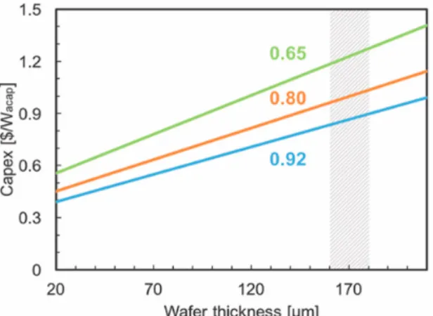
In addition, since the silicon wafer is the largest cost component in finished solar cells, it is widely accepted that a reduction of silicon wafer thickness without a decrease in yield will lower solar energy costs [3,4]. By using thinner wafers in manufacturing lines, polysilicon and crystal growth capex is reduced (proportionally with grams-of-silicon-per-watt); therefore, thin silicon has the potential to reduce poly-to-module capex by roughly 45% (see Fig. 1). The total capex is shown as a function of Si wafer thickness, which was varied between 20 and 210 µm, assuming different manufacturing yields from polysilicon to the final module (92%, 80% and 65%).
Si wafer thickness has decreased steadily over the years, but not as quickly as predicted despite the agreed cost benefits of thinner wafers. Handling and processing thin Si wafers (40 - 100 µm) is difficult and manufacturing yield is unacceptably low. Since micro-crack defects are more critical in thinner wafers due to the lower breakage force [5], they can seriously impede the solar cell performance and reliability of the module. On one side, the reduced thickness of the wafer implies that the wafer is more flexible, which means that the deflection is higher for the same applied force [6]. On the other side, the mechanical stress which can be applied to the wafer before failure decreases with wafer thickness. As a result, a crack will propagate from a smaller in-plane tensile stress when a force is applied normal to the crack plane (known as mode I fracture) [7]. In order to decrease the breakage rate of thinner wafers, the requirements for reducing mechanical loads during processing steps (e.g sawing, interconnection of cells, handling and transport) have to be adjusted. In addition, inline edge crack detection tools have to be improved and/or new techniques must be developed to allow for a non-destructive, fast, and accurate method of crack detection and characterization for thinner wafers with a wide variety of crack types [8].
State-of-the-art technologies for crack detection in silicon materials include: photoluminescence (PL) [9], optical transmission [10,11], infrared (IR) lock-in thermography (LIT) [12], scanning acoustic microscopy (SAM) [13], and dark-field IR scattering [14]. Although all these techniques are suitable for detecting cracks within the wafer, they have several disadvantages for detecting edge cracks; especially cracks with less than a few millimetres in length. In particular, PL has difficulty detecting edge cracks since the technique is based on measuring the reduction in minority carrier lifetimes, yet at early stages in cell fabrication, the edges themselves reduce the local lifetime [9]. Optical transmission is challenging because it relies on reduced transmission when a crack is present; thus, the method inherently has a low signal-to-noise ratio (SNR) [10,11]. LIT is a powerful technique that utilizes IR photons to generate a specific temperature pattern, but only cracks with tiny tips and a triangular shape at the surface can be detected [12]. In SAM, the image is generated due to acoustic impedance mismatch caused by micro-cracks, but only cracks 5 – 10 µm can be detected, neglecting larger cracks [13].
Light scattering is a non-invasive technique which allows us to determine structures down to the sub-micron scale with a high SNR. Industrially-available tools detect edge micro-cracks down to ~3 mm in length. However, for thin wafers less than 150 µm, there is a need for detection of even smaller cracks in order to avoid breakage during cell and module fabrication. As shown by Ortner et al. [14], cracks smaller than 1 mm in length can lead to a breakage of 20% of the wafer somewhere in the module production line. Thus, there is still an industrial need for improving edge crack detection tools. Enabling these tools requires a better understanding of the underlying physics of crack detection in order to overcome these limitations.
Building on the industrially-available dark-field light scattering approach described in [14], the goal of this work is to establish a reliable method for detecting edge micro-cracks by exploring the trade-off between field of view (FOV), incident light angle, and detectable crack length. Our new approach shows the potential to be used as a
Sarah Wieghold et al. / Energy Procedia 124 (2017) 526–531 527
Available online at www.sciencedirect.com
ScienceDirect
Energy Procedia 00 (2017) 000–000
www.elsevier.com/locate/procedia
1876-6102 © 2017 The Authors. Published by Elsevier Ltd.
Peer review by the scientific conference committee of SiliconPV 2017 under responsibility of PSE AG.
7th International Conference on Silicon Photovoltaics, SiliconPV 2017
Crack detection in crystalline silicon solar cells using dark-field
imaging
Sarah Wieghold
a, Ashley E. Morishige
a, Luke Meyer
a, Tonio Buonassisi
a, Emanuel M.
Sachs
a,*
aMassachusetts Institute of Technology, Cambridge, MA 02139, USA
Abstract
The high capital expenditure (capex) necessary to manufacture crystalline silicon PV modules negatively affects the levelized cost of electricity (¢/kWh) and critically impacts the rate at which the PV industry can scale up. Wafer, cell, and module fabrication with thin free-standing silicon wafers is one key to reduce capex. Thin wafers reduce capex associated with silicon refining and wafer fabrication, which together sum to 58% of the total capex of silicon module manufacturing. In addition, thin wafers directly and significantly reduce variable costs. However, introducing 50 μm thin free-standing wafers into today’s manufacturing lines result in cracking, creating a yield-based disincentive. Due to the brittle nature of silicon, wafer breakage is the major concern due to the high stress that is induced during processes in manufacturing lines. In this paper, we describe an improved method for edge micro-crack detection that can help enable low-capex, thin free-standing Si wafers. We present a method of detecting and measuring cracks along wafer edges by using a dark-field IR scattering imaging technique which enables detection of edge cracks at the micron scale.
© 2017 The Authors. Published by Elsevier Ltd.
Peer review by the scientific conference committee of SiliconPV 2017 under responsibility of PSE AG. Keywords: Capex; polysilicon; thin free-standing wafer; edge crack detection; IR scattering; dark-field imaging
* Corresponding author. Tel.: +1-617-253-5381
E-mail address: [email protected]
S. Wieghold/ Energy Procedia 00 (2017) 000–000
1. Introduction
One of the challenges in today’s photovoltaic (PV) industry is the high capital expenditure (capex) to manufacture crystalline silicon PV modules, which comprises ~22% of the minimum sustainable price of PV modules [1]. In addition, nearly 52% of silicon capex is embedded in polysilicon and wafer manufacturing, negatively affecting the cost-per-watt ($/W), levelized cost of electricity (LCOE) (¢/kWh),and preventing the scale up of the PV industry (ref. [1] for the year 2015). To reduce this market limitation, approaches to reduce capex have been developed [2] and include: i) increase of tool throughput e.g. production volume and yield (m2 per unit time),
ii) improvement of solar cell conversion efficiency (W per m2), and iii) reduction of silicon usage per wafer. Kerfless
technologies represent a promising approach to reduce the required amount of silicon, since wafer with the same thickness can be produced with less silicon compared to the standard ingot-based growth methods.
In addition, since the silicon wafer is the largest cost component in finished solar cells, it is widely accepted that a reduction of silicon wafer thickness without a decrease in yield will lower solar energy costs [3,4]. By using thinner wafers in manufacturing lines, polysilicon and crystal growth capex is reduced (proportionally with grams-of-silicon-per-watt); therefore, thin silicon has the potential to reduce poly-to-module capex by roughly 45% (see Fig. 1). The total capex is shown as a function of Si wafer thickness, which was varied between 20 and 210 µm, assuming different manufacturing yields from polysilicon to the final module (92%, 80% and 65%).
Si wafer thickness has decreased steadily over the years, but not as quickly as predicted despite the agreed cost benefits of thinner wafers. Handling and processing thin Si wafers (40 - 100 µm) is difficult and manufacturing yield is unacceptably low. Since micro-crack defects are more critical in thinner wafers due to the lower breakage force [5], they can seriously impede the solar cell performance and reliability of the module. On one side, the reduced thickness of the wafer implies that the wafer is more flexible, which means that the deflection is higher for the same applied force [6]. On the other side, the mechanical stress which can be applied to the wafer before failure decreases with wafer thickness. As a result, a crack will propagate from a smaller in-plane tensile stress when a force is applied normal to the crack plane (known as mode I fracture) [7]. In order to decrease the breakage rate of thinner wafers, the requirements for reducing mechanical loads during processing steps (e.g sawing, interconnection of cells, handling and transport) have to be adjusted. In addition, inline edge crack detection tools have to be improved and/or new techniques must be developed to allow for a non-destructive, fast, and accurate method of crack detection and characterization for thinner wafers with a wide variety of crack types [8].
State-of-the-art technologies for crack detection in silicon materials include: photoluminescence (PL) [9], optical transmission [10,11], infrared (IR) lock-in thermography (LIT) [12], scanning acoustic microscopy (SAM) [13], and dark-field IR scattering [14]. Although all these techniques are suitable for detecting cracks within the wafer, they have several disadvantages for detecting edge cracks; especially cracks with less than a few millimetres in length. In particular, PL has difficulty detecting edge cracks since the technique is based on measuring the reduction in minority carrier lifetimes, yet at early stages in cell fabrication, the edges themselves reduce the local lifetime [9]. Optical transmission is challenging because it relies on reduced transmission when a crack is present; thus, the method inherently has a low signal-to-noise ratio (SNR) [10,11]. LIT is a powerful technique that utilizes IR photons to generate a specific temperature pattern, but only cracks with tiny tips and a triangular shape at the surface can be detected [12]. In SAM, the image is generated due to acoustic impedance mismatch caused by micro-cracks, but only cracks 5 – 10 µm can be detected, neglecting larger cracks [13].
Light scattering is a non-invasive technique which allows us to determine structures down to the sub-micron scale with a high SNR. Industrially-available tools detect edge micro-cracks down to ~3 mm in length. However, for thin wafers less than 150 µm, there is a need for detection of even smaller cracks in order to avoid breakage during cell and module fabrication. As shown by Ortner et al. [14], cracks smaller than 1 mm in length can lead to a breakage of 20% of the wafer somewhere in the module production line. Thus, there is still an industrial need for improving edge crack detection tools. Enabling these tools requires a better understanding of the underlying physics of crack detection in order to overcome these limitations.
Building on the industrially-available dark-field light scattering approach described in [14], the goal of this work is to establish a reliable method for detecting edge micro-cracks by exploring the trade-off between field of view (FOV), incident light angle, and detectable crack length. Our new approach shows the potential to be used as a
528 Sarah Wieghold et al. / Energy Procedia 124 (2017) 526–531
S. Wieghold/ Energy Procedia 00 (2017) 000–000
screening tool or as inline modification in existing industry tools, detecting micro-cracks less than a millimeter in length.
2. Experimental
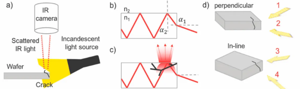
Multicrystalline silicon (mc-Si) wafers with a thickness of 180 µm were used. Edge cracks were either intentionally induced or wafers with known cracks were used. For detecting edge cracks, a broad-response InGaAs camera (320 256-pixel array) was employed in a dark-field IR scattering setup (Fig. 2a). Since the spatial resolution of the camera is limited by optics and the pixel array, a 5 objective was equipped with different extension tubes (80 mm, 50 mm, 25 mm, and 15 mm) for high-resolution images. An incandescent light source was used for edge illumination, and the incident angle was varied.
3. Results and discussion
3.1. Capex as a function of wafer thickness
Fig. 1 shows the calculated capex as a function of wafer thickness for mc-Si assuming different manufacturing yields. Capex was calculated with the bottom-up cost model which includes market conditions and technology for the first half of 2015 (1H-2015) (the model can be downloaded from [15] and can be found in the ESI of [1]).
Fig. 1. Total silicon PV capex as a function of wafer thickness, assuming constant yield from polysilicon to module (blue: 92%, orange: 80% and green: 65%). The grey lines indicate current wafer thicknesses used in PV industry.
3.2. Dark-field IR scattering setup
A schematic of the dark-field IR scattering setup is shown in Fig. 2a. In this configuration, the wafer edge is illuminated from the side with an incandescent light source. If the angle of incidence of the incoming light beam is above the critical angle, total internal reflection (TIR) occurs at the interface of materials with two different refractive indices n1 and n2 (Fig. 2b). Refractive indices for silicon and air are 3.7 (at 800 nm) and 1, respectively, so
TIR is achieved with an incident angle of ~13. Hence, the light is reflected at the interface and the radiation is confined and propagates within the bulk. If a crack is present, elastic scattering (Rayleigh scattering) occurs at the crack and the light changes direction compared to the incident light. The requirements of TIR are not fulfilled anymore and the light can exit the sample surface (Fig. 2c) and can be detected by the camera.
S. Wieghold/ Energy Procedia 00 (2017) 000–000
3.3 Dark-field IR scattering images
As proof of concept, an edge crack of a mc-Si wafer was imaged under different light directions, maintaining TIR conditions. Here, cracks were imaged perpendicular and in-line with the illumination direction under different entering conditions to investigate the scattering behavior and intensity (compare configuration for imaging in Fig. 2d). In general, the presence of a crack is measured by scattering events along its length and can be seen as bright spots. The scattering intensity strongly depends on the light direction when imaged under TIR conditions.
Fig. 2. (a) Schematic of the edge micro-crack detection setup equipped with an InGaAs camera and an incandescent light source; (b) and (c) physics of TIR at an interface with different refractive indices, adapted from ref. 14. Refractive indices for silicon (n1) and air (n2) are 3.7 (at
800 nm) and 1, respectively. (d) Schematic of the imaging conditions perpendicular and in-line with the crack propagation direction. The light is coupled into the substrate under TIR conditions at an entering angle of 13 either from the front side for configuration 1 and 3 or from the rear side for configuration 2 and 4.
The images shown in Fig. 3a and 3b were imaged from the side, thus perpendicular to the crack direction (also compare Fig 2d, perpendicular configuration) at an entering angle of 13 which fulfils the TIR conditions. The images were taken with a 5 objective and an 80 mm extension tube resulting in a FOV of 5.7 µm/pixel. Fig 3a was imaged from the side, the light source pointed downwards to the wafer edge (configuration 1). Image 3b was measured with the light source pointing upwards from the side of the wafer edge (configuration 2). The images shown in Fig. 3c and 3d were imaged under front illumination, in-line with the crack propagation direction (compare in-line configuration in Fig. 2d). Fig. 3c was imaged under front illumination of the wafer edge from the top (the light source was pointed downwards, configuration 3) whereas 3d was imaged in a configuration where the light source was pointed upwards to the wafer edge.
Fig. 3. Scattering images taken with a 5x objective and an extension tube of 80 mm under different light illumination direction at TIR conditions. (a) and (b) Light direction perpendicular to the crack propagation direction with illumination from the front (a) and the rear side (b); conditions shown in fig. 2d perpendicular, conditions 1 and 2. (c) and (d) light direction in-line with the crack propagation direction with illumination from the front (c) and from the rear side (d), compare conditions fig. 2d in-line, conditions 3 and 4.
Comparing all different light direction scenarios, the scattering intensity strongly depends on the direction of edge illumination related to the crack direction, measured under TIR conditions. If the crack is illuminated perpendicular to the crack propagation direction, the highest light scattering intensity and contrast is achieved as can be seen in Fig. 3a. Further, illumination from the top seems to be more suitable for our scattering setup. One possibility why cracks illuminated from the top show an enhanced intensity could be related to their scattering behavior. Cracks with rather
Sarah Wieghold et al. / Energy Procedia 124 (2017) 526–531 529
S. Wieghold/ Energy Procedia 00 (2017) 000–000
screening tool or as inline modification in existing industry tools, detecting micro-cracks less than a millimeter in length.
2. Experimental
Multicrystalline silicon (mc-Si) wafers with a thickness of 180 µm were used. Edge cracks were either intentionally induced or wafers with known cracks were used. For detecting edge cracks, a broad-response InGaAs camera (320 256-pixel array) was employed in a dark-field IR scattering setup (Fig. 2a). Since the spatial resolution of the camera is limited by optics and the pixel array, a 5 objective was equipped with different extension tubes (80 mm, 50 mm, 25 mm, and 15 mm) for high-resolution images. An incandescent light source was used for edge illumination, and the incident angle was varied.
3. Results and discussion
3.1. Capex as a function of wafer thickness
Fig. 1 shows the calculated capex as a function of wafer thickness for mc-Si assuming different manufacturing yields. Capex was calculated with the bottom-up cost model which includes market conditions and technology for the first half of 2015 (1H-2015) (the model can be downloaded from [15] and can be found in the ESI of [1]).
Fig. 1. Total silicon PV capex as a function of wafer thickness, assuming constant yield from polysilicon to module (blue: 92%, orange: 80% and green: 65%). The grey lines indicate current wafer thicknesses used in PV industry.
3.2. Dark-field IR scattering setup
A schematic of the dark-field IR scattering setup is shown in Fig. 2a. In this configuration, the wafer edge is illuminated from the side with an incandescent light source. If the angle of incidence of the incoming light beam is above the critical angle, total internal reflection (TIR) occurs at the interface of materials with two different refractive indices n1 and n2 (Fig. 2b). Refractive indices for silicon and air are 3.7 (at 800 nm) and 1, respectively, so
TIR is achieved with an incident angle of ~13. Hence, the light is reflected at the interface and the radiation is confined and propagates within the bulk. If a crack is present, elastic scattering (Rayleigh scattering) occurs at the crack and the light changes direction compared to the incident light. The requirements of TIR are not fulfilled anymore and the light can exit the sample surface (Fig. 2c) and can be detected by the camera.
S. Wieghold/ Energy Procedia 00 (2017) 000–000
3.3 Dark-field IR scattering images
As proof of concept, an edge crack of a mc-Si wafer was imaged under different light directions, maintaining TIR conditions. Here, cracks were imaged perpendicular and in-line with the illumination direction under different entering conditions to investigate the scattering behavior and intensity (compare configuration for imaging in Fig. 2d). In general, the presence of a crack is measured by scattering events along its length and can be seen as bright spots. The scattering intensity strongly depends on the light direction when imaged under TIR conditions.
Fig. 2. (a) Schematic of the edge micro-crack detection setup equipped with an InGaAs camera and an incandescent light source; (b) and (c) physics of TIR at an interface with different refractive indices, adapted from ref. 14. Refractive indices for silicon (n1) and air (n2) are 3.7 (at
800 nm) and 1, respectively. (d) Schematic of the imaging conditions perpendicular and in-line with the crack propagation direction. The light is coupled into the substrate under TIR conditions at an entering angle of 13 either from the front side for configuration 1 and 3 or from the rear side for configuration 2 and 4.
The images shown in Fig. 3a and 3b were imaged from the side, thus perpendicular to the crack direction (also compare Fig 2d, perpendicular configuration) at an entering angle of 13 which fulfils the TIR conditions. The images were taken with a 5 objective and an 80 mm extension tube resulting in a FOV of 5.7 µm/pixel. Fig 3a was imaged from the side, the light source pointed downwards to the wafer edge (configuration 1). Image 3b was measured with the light source pointing upwards from the side of the wafer edge (configuration 2). The images shown in Fig. 3c and 3d were imaged under front illumination, in-line with the crack propagation direction (compare in-line configuration in Fig. 2d). Fig. 3c was imaged under front illumination of the wafer edge from the top (the light source was pointed downwards, configuration 3) whereas 3d was imaged in a configuration where the light source was pointed upwards to the wafer edge.
Fig. 3. Scattering images taken with a 5x objective and an extension tube of 80 mm under different light illumination direction at TIR conditions. (a) and (b) Light direction perpendicular to the crack propagation direction with illumination from the front (a) and the rear side (b); conditions shown in fig. 2d perpendicular, conditions 1 and 2. (c) and (d) light direction in-line with the crack propagation direction with illumination from the front (c) and from the rear side (d), compare conditions fig. 2d in-line, conditions 3 and 4.
Comparing all different light direction scenarios, the scattering intensity strongly depends on the direction of edge illumination related to the crack direction, measured under TIR conditions. If the crack is illuminated perpendicular to the crack propagation direction, the highest light scattering intensity and contrast is achieved as can be seen in Fig. 3a. Further, illumination from the top seems to be more suitable for our scattering setup. One possibility why cracks illuminated from the top show an enhanced intensity could be related to their scattering behavior. Cracks with rather
530 Sarah Wieghold et al. / Energy Procedia 124 (2017) 526–531
S. Wieghold/ Energy Procedia 00 (2017) 000–000
flat internal surfaces do not scatter light omnidirectionally [14]; thus, the light reflection could exit the wafer surface opposite to the camera.
Fig. 4. Scattering images taken of the same crack as in fig. 3 with a 5X objective and different extension tubes resulting in different field of views: (a) 50 mm; (b) 25 mm; (c) 15 mm; and (d) bare 5X objective.
To determine the spatial resolution of our setup as a function of field of view (FOV), we used a 5 objective equipped with different extension tube lengths (Fig. 4). Scattering images taken with a 5 objective and the following extension tubes are shown: 50 mm (a), 25 mm (b), 15 mm (c), and no extension tube (d). To evaluate the images, the same edge crack is imaged as shown in Fig. 3, which was taken with an 80 mm extension tube. As seen in Fig. 4a, a high-resolution scattering image of the crack is achieved, revealing a V-shape of the crack directly at the edge of the wafer. By decreasing the extension tubes and therefore increasing the FOV, this feature can not be resolved anymore and is superimposed by edge light scattering at the crack (Fig. 4b-d). In addition, the overall scattering intensity decreases with an increased FOV. Note, that no scattering at grains and grain boundaries is visible, which is due to the similar refractive indices and absorption of grains [14]. However, additional bright spots are seen in the images which are due to surface impurities causing additional reflection. One possibility to eliminate false positive results in our setup is to decouple surface features from cracks. For example, this can be done by using different filters or by using different light sources. The idea is that photons with a higher energy than 1.1 eV will be absorbed and reflected by the silicon surface whereas photons with a lower energy than 1.1 eV will be transmitted, scattered at a crack, and reflected by the Si surface. By taking two images and subsequently subtracting the images, one can unambiguously distinguish a surface crack from a surface feature.
4. Conclusion
In this contribution, we present a method for detection edge micro-cracks with a high SNR. Since there is still an industrial need for improved crack detection tools, we used an approach based on a better understanding of the underlying physics of crack detection. By using a modified imaging approach, we determined the trade-off between FOV, incident light angle, and light direction. By varying the illumination direction (e.g. perpendicular or in-line with the crack propagation direction), we could increase the sensitivity of edge crack detection. Our presented approach has the potential to detect cracks which are smaller than 500 m in length, which shows an increased resolution of 4-6 times compared to industry-available tools. Since the critical crack length will decrease for thinner wafers due to a lower breakage force, it is even more important to modify and develop additional inline crack detection tools. However, we also note that for industry applications, the screening throughput of wafers has to be increased as well as the sensitivity to unambiguously distinguish between a surface feature and a crack to avoid false positive results in a manufacturing line.
Acknowledgements
This work was supported by the DOE under award no. DE-EE0007535. This work was performed in part at the Harvard University Center for Nanoscale Systems (CNS), a member of the National Nanotechnology Coordinated Infrastructure Network (NNCI), which is supported by the National Science Foundation under NSF EECS award no. 1541959.
S. Wieghold/ Energy Procedia 00 (2017) 000–000
References
[1] Powell DM, Fu R, Horowitz K, Basore PA, Woodhouse M, Buonassisi T. The capital intensity of photovoltaics manufacturing: barrier to scale and opportunity for innovation. Energy Env Sci 2015;8:3395–408.
[2] del Canizo C, del Coso G, Sinke WC. Crystalline silicon solar module technology: towards the 1€ per watt-peak goal. Prog Photovolt Res Appl 2009;178:199–209.
[3] Münzer KA, Holdermann KT, Schlosser RE, Sterk S. Thin Monocrystalline Silicon Solar Cells. IEEE Trans Electron Devices 1999; 46:2055-61.
[4] Bruton TM. General trends about photovoltaics based on crystalline silicon. Sol Energ Mat Sol Cells 2002;72:3–10.
[5] Coletti G, van der Borg NJCM, De Iuliis S, Tool CJJ, Geerligs LJ. Mechanical strength of silicon wafers depending on wafer thickness and surface treatment. Presented at the 21st European Photovoltaic Solar Energy Conference and Exhibition 2006, Dresden, Germany. [6] Wang PA. Industrial challenges for thin wafer manufacturing. Conference record of the 2006 IEEE 4th World Conference on Photovoltaic
Energy Conversion 2006, HI, p. 1179–82.
[7] Brun XF, Melkote SN. Analysis of stresses and breakage of crystalline silicon wafers during handling and transport. Sol Energ Mat Sol Cells 2009;93:1238-47.
[8] Abdelhamid M, Singh R, Omar M. Review of microcrack detection techniques for silicon silar cells. IEEE J Photovolt 2014;4:514-24. [9] Trupke T, Bardos RA, Schubert MC, Warta W. Photoluminescence imaging of silicon wafers. Appl Phys Lett 2006;89:44107-3.
[10] Li B, Xianghao H, Shuai F. Automatic inspection of surface crack in solar cell images. Chinese Control and Decision Conference 2011, p. 993-98.
[11] Rueland E, Herguth A, Trummer A, Wansleben S, Fath P. Microcrack detection and other optical characterization techniques for in-line inspection of wafers and cells. Proceedings of the 20th European Photovoltaic Solar Energy Conference and Exhibition 2005, Barcelona, Spain, p. 3242–45.
[12] Breitenstein O, Langenkamp M, Lang O, Schirrmacher A. Shunts due to laser scribing of solar cell evaluated by highly sensitive lock-in thermography. Sol Energ Mat Sol Cells 2001;65:55-62.
[13] Belyaev A, Polupan O, Ostapenko S, Hess DP, Kalejs JP. Resonance ultrasonic vibration diagnostics of elastic stress in full-size silicon wafers. Semicond Sci Technol 2006;21:254-60.
[14] Ortner A, Gräff O, Stelzl M, Macherey F, Neubecker R. Edge-light: combination of sensitive crack detection and luminescence measurements. Prog Photovolt Res Appl 2013;21:1343-53.
Sarah Wieghold et al. / Energy Procedia 124 (2017) 526–531 531
S. Wieghold/ Energy Procedia 00 (2017) 000–000
flat internal surfaces do not scatter light omnidirectionally [14]; thus, the light reflection could exit the wafer surface opposite to the camera.
Fig. 4. Scattering images taken of the same crack as in fig. 3 with a 5X objective and different extension tubes resulting in different field of views: (a) 50 mm; (b) 25 mm; (c) 15 mm; and (d) bare 5X objective.
To determine the spatial resolution of our setup as a function of field of view (FOV), we used a 5 objective equipped with different extension tube lengths (Fig. 4). Scattering images taken with a 5 objective and the following extension tubes are shown: 50 mm (a), 25 mm (b), 15 mm (c), and no extension tube (d). To evaluate the images, the same edge crack is imaged as shown in Fig. 3, which was taken with an 80 mm extension tube. As seen in Fig. 4a, a high-resolution scattering image of the crack is achieved, revealing a V-shape of the crack directly at the edge of the wafer. By decreasing the extension tubes and therefore increasing the FOV, this feature can not be resolved anymore and is superimposed by edge light scattering at the crack (Fig. 4b-d). In addition, the overall scattering intensity decreases with an increased FOV. Note, that no scattering at grains and grain boundaries is visible, which is due to the similar refractive indices and absorption of grains [14]. However, additional bright spots are seen in the images which are due to surface impurities causing additional reflection. One possibility to eliminate false positive results in our setup is to decouple surface features from cracks. For example, this can be done by using different filters or by using different light sources. The idea is that photons with a higher energy than 1.1 eV will be absorbed and reflected by the silicon surface whereas photons with a lower energy than 1.1 eV will be transmitted, scattered at a crack, and reflected by the Si surface. By taking two images and subsequently subtracting the images, one can unambiguously distinguish a surface crack from a surface feature.
4. Conclusion
In this contribution, we present a method for detection edge micro-cracks with a high SNR. Since there is still an industrial need for improved crack detection tools, we used an approach based on a better understanding of the underlying physics of crack detection. By using a modified imaging approach, we determined the trade-off between FOV, incident light angle, and light direction. By varying the illumination direction (e.g. perpendicular or in-line with the crack propagation direction), we could increase the sensitivity of edge crack detection. Our presented approach has the potential to detect cracks which are smaller than 500 m in length, which shows an increased resolution of 4-6 times compared to industry-available tools. Since the critical crack length will decrease for thinner wafers due to a lower breakage force, it is even more important to modify and develop additional inline crack detection tools. However, we also note that for industry applications, the screening throughput of wafers has to be increased as well as the sensitivity to unambiguously distinguish between a surface feature and a crack to avoid false positive results in a manufacturing line.
Acknowledgements
This work was supported by the DOE under award no. DE-EE0007535. This work was performed in part at the Harvard University Center for Nanoscale Systems (CNS), a member of the National Nanotechnology Coordinated Infrastructure Network (NNCI), which is supported by the National Science Foundation under NSF EECS award no. 1541959.
S. Wieghold/ Energy Procedia 00 (2017) 000–000
References
[1] Powell DM, Fu R, Horowitz K, Basore PA, Woodhouse M, Buonassisi T. The capital intensity of photovoltaics manufacturing: barrier to scale and opportunity for innovation. Energy Env Sci 2015;8:3395–408.
[2] del Canizo C, del Coso G, Sinke WC. Crystalline silicon solar module technology: towards the 1€ per watt-peak goal. Prog Photovolt Res Appl 2009;178:199–209.
[3] Münzer KA, Holdermann KT, Schlosser RE, Sterk S. Thin Monocrystalline Silicon Solar Cells. IEEE Trans Electron Devices 1999; 46:2055-61.
[4] Bruton TM. General trends about photovoltaics based on crystalline silicon. Sol Energ Mat Sol Cells 2002;72:3–10.
[5] Coletti G, van der Borg NJCM, De Iuliis S, Tool CJJ, Geerligs LJ. Mechanical strength of silicon wafers depending on wafer thickness and surface treatment. Presented at the 21st European Photovoltaic Solar Energy Conference and Exhibition 2006, Dresden, Germany. [6] Wang PA. Industrial challenges for thin wafer manufacturing. Conference record of the 2006 IEEE 4th World Conference on Photovoltaic
Energy Conversion 2006, HI, p. 1179–82.
[7] Brun XF, Melkote SN. Analysis of stresses and breakage of crystalline silicon wafers during handling and transport. Sol Energ Mat Sol Cells 2009;93:1238-47.
[8] Abdelhamid M, Singh R, Omar M. Review of microcrack detection techniques for silicon silar cells. IEEE J Photovolt 2014;4:514-24. [9] Trupke T, Bardos RA, Schubert MC, Warta W. Photoluminescence imaging of silicon wafers. Appl Phys Lett 2006;89:44107-3.
[10] Li B, Xianghao H, Shuai F. Automatic inspection of surface crack in solar cell images. Chinese Control and Decision Conference 2011, p. 993-98.
[11] Rueland E, Herguth A, Trummer A, Wansleben S, Fath P. Microcrack detection and other optical characterization techniques for in-line inspection of wafers and cells. Proceedings of the 20th European Photovoltaic Solar Energy Conference and Exhibition 2005, Barcelona, Spain, p. 3242–45.
[12] Breitenstein O, Langenkamp M, Lang O, Schirrmacher A. Shunts due to laser scribing of solar cell evaluated by highly sensitive lock-in thermography. Sol Energ Mat Sol Cells 2001;65:55-62.
[13] Belyaev A, Polupan O, Ostapenko S, Hess DP, Kalejs JP. Resonance ultrasonic vibration diagnostics of elastic stress in full-size silicon wafers. Semicond Sci Technol 2006;21:254-60.
[14] Ortner A, Gräff O, Stelzl M, Macherey F, Neubecker R. Edge-light: combination of sensitive crack detection and luminescence measurements. Prog Photovolt Res Appl 2013;21:1343-53.