HAL Id: hal-01847901
https://hal.laas.fr/hal-01847901
Submitted on 24 Jul 2018
HAL is a multi-disciplinary open access
archive for the deposit and dissemination of sci-entific research documents, whether they are pub-lished or not. The documents may come from teaching and research institutions in France or abroad, or from public or private research centers.
L’archive ouverte pluridisciplinaire HAL, est destinée au dépôt et à la diffusion de documents scientifiques de niveau recherche, publiés ou non, émanant des établissements d’enseignement et de recherche français ou étrangers, des laboratoires publics ou privés.
Design of building blocks of power management system
for a reconfigurable structure of supercapacitors
Aris Siskos
To cite this version:
Aris Siskos. Design of building blocks of power management system for a reconfigurable structure of supercapacitors. Micro and nanotechnologies/Microelectronics. 2017. �hal-01847901�
Design of building blocks of power
management system for a reconfigurable
structure of supercapacitors
Aris Siskos
Supervised by: Marise Bafleur
Toulouse July 2017
2
Contents
1 Problem Analysis, System Description and Proposed Solution ... 7
1.1 Problem Analysis ... 7
1.2 System Specifications and Challenges ... 9
1.2.1 Challenges ... 9
1.2.2 Specifications and restrictions ... 10
1.3 Proposed Architecture ... 11
1.3.1 Power management unit ... 12
1.3.2 Control unit ... 12
1.3.3 Complementary circuits. ... 13
2 Circuit blocks ... 14
2.1 Switches ... 14
2.2 Bias circuit ... 15
2.2.1 Bias circuit design ... 15
2.2.2 Bias circuit simulation results ... 16
2.3 Comparators and delay lines ... 18
2.3.1 Comparator design ... 18
2.3.2 Comparator simulation results ... 19
2.3.3 Delay line ... 20
2.4 LDO ... 21
2.4.1 LDO design ... 22
2.4.2 LDO simulation results ... 24
2.5 Bandgap reference and Buffer ... 31
2.5.1 Bandgap reference design ... 32
2.5.2 Bandgap reference simulation results ... 33
2.5.3 Buffer design ... 37
2.5.4 Buffer simulation results ... 38
3 System architecture and layout design ... 40
3.1 System architecture design. ... 40
3.1.1 Delay capacitors ... 41
3.1.2 Voltage divider for threshold voltages ... 42
3.1.3 Reference node of comparators ... 42
3 3.2.1 Switch Interconnections ... 44 3.2.2 Matching techniques. ... 44 3.2.3 System simulation ... 47 Charging ... 47 Discharging ... 50 4 Chip Design ... 53
4.1 New architecture of LDO ... 53
4.1.1 New LDO simulation results ... 55
4.2 System ... 58
4.2.1 New system simulation results ... 58
Charging ... 58
Discharging ... 59
4
List of Figures
Figure 1. General model of 2N SCs structure [1]. ... 7
Figure 2. Four SCs structure with the switches derived from the general model [2]. ... 7
Figure 3. Charging phase of the SCs structured compared with fixed C/4 and fixed C*4 capacitors [2]. .... 8
Figure 4. Discharging phase of the SCs structured compared with fixed C/4 and fixed C*4 capacitors [2]. 8 Figure 5. General architecture of the system. ... 9
Figure 6. Proposed architecture of the system. ... 11
Figure 7. Bulk regulation technique for PMOS switch. ... 15
Figure 8. Bias circuit architecture. ... 16
Figure 9. Power consumption of bias circuit for different supply voltages and temperatures in typical condition. ... 17
Figure 10. Power consumption of the bias circuit for different supply voltages and temperatures in worst speed condition. ... 17
Figure 11. Proposed architecture for both comparators. ... 18
Figure 12. Transient response of the comparator in the output in typical condition, when a sine at the input is applied. ... 20
Figure 13. Transient response of the comparator in the output in worst speed condition, when a sine at the input is applied. ... 20
Figure 14. Delay line architecture. ... 21
Figure 15. Topology of a classic LDO. ... 21
Figure 16. Operation regions of LDO. ... 22
Figure 17. Proposed architecture of the error amplifier of LDO with the pass device. ... 23
Figure 18. Output of LDO, when supply voltage and temperature vary. ... 27
Figure 19. PSRR of LDO for different supply voltages in typical condition ... 27
Figure 20. PSRR of LDO for different supply voltages in worst one condition ... 28
Figure 21. Gain Bandwidth and Phase Margin of LDO in typical condition. ... 28
Figure 22. Gain Bandwidth and Phase Margin of LDO in worst zero. ... 29
Figure 23. Transient analysis of LDO when the input voltage VIN and load current ILOAD variations in typical condition. ... 30
Figure 24. Transient analysis of LDO when the input voltage VIN and load currentILOAD variations in worst one condition. ... 30
Figure 25. Architecture for the bandgap reference circuit proposed in [8]. ... 32
Figure 26. Temperature dependence of the bandgap reference circuit in typical condition. ... 35
Figure 27. Temperature dependence of the bandgap reference circuit in worst zero condition. ... 36
Figure 28. PSRR result of the bandgap reference in typical condition. ... 36
Figure 29. PSRR result of the bandgap reference in worst speed condition. ... 37
Figure 30. Architecture of the buffer. ... 37
Figure 31. PSRR results of buffer in typical condition. ... 38
Figure 32. . PSRR results of buffer in worst one condition. ... 39
Figure 33. Final proposed architecture of the reconfigurable SCs system. ... 40
Figure 34. Physical design of the system. ... 43
Figure 35. Metal slots in metal 3 layer for a large metal width interconnection ... 44
Figure 36. (a) Common centroid technique. (b) Symmetry. (c) Guard rings [9]. ... 45
5
Figure 38. Integiditated technique for the symmetric resistance of bandgap core. ... 46
Figure 39. Dummy devices placed in the edges of a transistor with fingers. ... 46
Figure 40. Guard ring around the bandgap core, which is a sensitive circuit. ... 47
Figure 41. The charging of the system for 700μΑ current compared with a fixed 400mF capacitor. ... 48
Figure 42. The charging of the system for 15mΑ current compared with a fixed 400mF capacitor. ... 48
Figure 43. Worst speed condition analysis for charging current 700μΑ. ... 49
Figure 44. Worst zero condition analysis for charging current 15mA. ... 49
Figure 45. The shape of the oscillation. ... 50
Figure 46. The discharging of the system for 2μA current. ... 50
Figure 47.The discharging of the system for 50mΑ current compared with a fixed 400mF capacitor. ... 51
Figure 48.Worst one condition analysis for discharging current 2μΑ. ... 51
Figure 49. Worst one condition analysis for discharging current 50mΑ. ... 52
Figure 50. The architecture of the LDO in C35B4C3. ... 54
Figure 51. PSRR of the new LDO for different supply voltages in typical condition ... 56
Figure 52. Bandwidth and phase margin of the new LDO for different supply voltages in typical condition ... 57
Figure 53. Transient response of new LDO in typical condition ... 57
Figure 54. Physical design of the final CHIP ... 58
Figure 55. The charging of the new system for 700μΑ current compared with a fixed 400mF capacitor. 59 Figure 56. The charging of the new system for 15mΑ current compared with a fixed 400mF capacitor. . 59
Figure 57. The discharging of the new system for 2μΑ current. ... 60
Figure 58. The discharging of the new system for 30mΑ current compared with a fixed 400mF capacitor. ... 60
6
List of Tables
Table 1. Sizes of the elements of bias circuit. ... 16
Table 2. Sizes of the elements of the comparator. ... 19
Table 3. Sizes of the elements of the LDO ... 24
Table 4. Results of LDO in typical condition. ... 25
Table 5. Results of LDO in worst power condition. ... 25
Table 6. Results of LDO in worst speed condition. ... 25
Table 7. Results of LDO in worst one condition. ... 26
Table 8. Results of LDO in worst zero condition. ... 26
Table 9. Sizes of the elements of the bandgap reference circuit ... 33
Table 10. Typical performance of the bandgap reference circuit ... 34
Table 11. Performance of the bandgap reference circuit in the worst power condition (low temperature) ... 34
Table 12. Performance of the bandgap reference circuit in the worst speed condition (high temperature) ... 34
Table 13. Performance of the bandgap reference circuit in the worst one condition ... 35
Table 14. Performance of the bandgap reference circuit in the worst case zero ... 35
Table 15. Sizes of the elements of buffer circuit ... 38
Table 16. Sizes of the elements of the new LDO design ... 54
Table 17. Results of new LDO in typical condition. ... 55
Table 18. Results of new LDO in worst power condition. ... 55
Table 19. Results of new LDO in worst speed condition. ... 55
Table 20. Results of new LDO in worst one condition. ... 56
7
1 Problem Analysis, System Description and Proposed Solution
The goal of this work is to implement an IC power management unit that will control a reconfigurable structure of supercapacitors (SCs) bank and supply different loads. In the sub-chapter the problem will be analyzed, a solution for this problem will be proposed and the system that meet the specifications of the problem will be described.
1.1 Problem Analysis
In [1] is presented a general model of the SCs reconfigurable bank, where there are distinct states of the SCs (figure 1). These states are distinguished among three categories of configurations, the all-series (AS) configuration, the series-parallel (SP) configurations and the all-parallel configuration (AP).
Figure 1. General model of 2N SCs structure [1].
This model considers that one storage media is at order 1 and 2N SCs are at order N. Then, for an N order system, N+1 distinct states are necessary and 3*(2N-1) switches are used to change the states. In [1] is highlighted that the optimum number of SCs is 2N=4, as the higher energy utilization is achieved with the lowest complexity. Nine switches and three different states are necessary for four SCs structure, as it is illustrated in figure 2.
8
The four SCs model has been implemented and validated with discrete devices in [2]. The advantage of the reconfigurable bank of SCs compared to a fixed capacitor is that the charging and the discharging times are shorter and longer respectively. This is shown in figure 3, where the reconfigurable structure reaches faster a higher potential during charging than an equivalent with the SCs connected in AP configuration fixed capacitor. In addition, the reconfigurable structure needs longer time to discharge than the equivalent fixed capacitor, providing more energy to the load.
Figure 3. Charging phase of the SCs structured compared with fixed C/4 and fixed C*4 capacitors [2].
Figure 4. Discharging phase of the SCs structured compared with fixed C/4 and fixed C*4 capacitors [2].
While the structure is charging, it manages to obtain enough voltage across the all-series connection to supply the load. In addition, the discharging in the current structure offers available energy for longer time compared to the fixed capacitor. Moreover, this structure proves that losses in the switches and the control circuit are less than the available power that is gained.
The control unit of this discrete system is simple as it extracts from the fourth capacitor a voltage, which is compared with a reference voltage by two comparators, where each one is responsible to change the configuration. The first comparator with the low voltage threshold at its input changes the structure from
9 AS to SP configuration and vice versa and the second comparator with the high voltage threshold in his input changes the structure from SP configuration to AP configuration and vice versa.
Comparable to the general model is also a structure that is implemented with discrete components, which has six SCs and four states. Also, it uses fifteen switches which are controlled by three signals and the complementary of them [3]. Despite of the simplicity of the control unit, the high number of switches might introduce significant losses in the system.
In this work we implemented an IC design of the power management and control unit of general model with four SC. The control unit is responsible to set the switches properly in order to alter the configurations when specific voltage level prevail in the SCs. The power management unit is responsible to supply different loads, with the minimum possible fluctuations. In wireless sensor network (WSN) systems, loads are usually communication nodes (transceivers, antennas etc.), signal conditioning circuits or other circuits, which implement specific functions. The energy of the SCs have to be sufficient in order to supply the load for the longest time possible.
The general system can be described in a block diagram, as it is shown in figure 5.
Energy Harvester Regulator Unit Load Control Unit Reconfigurable Storage
Figure 5. General architecture of the system.
1.2 System Specifications and Challenges
The system architecture design requires different steps. The first step is the answer to the question of how and where the system is ought to operate. The second step is to set the specifications and restrictions, which are exported from the application targets. The last step is the proposal of an architecture that can operate with the current specifications and restrictions.
1.2.1 Challenges
A power management system for a WSN that is powered by an energy harvesting system has to be autonomous. For autonomy it is crucial the circuits to be very low power. Another challenge is the capability of the system to be as generic as possible.
Autonomy is achieved when the system is able to charge the SCs starting from AS configuration and the SCs obtain the maximum energy in AP configuration. That implies that the system has to self-startup, so
10
that the SCs start charging. Also, the control management and the power management unit, need to consume energy from the SCs.
In view of the fact that all the circuits are supplied from the SCs, their design have to be very low power. That means the consumption is of some hundreds nA to a few μΑ. This is a crucial challenge, when the system is being designed, as it introduces limitations in the operation.
A generic system is achieved if the operation range of the circuit in both charging and discharging is wide. The system has to charge with various energy sources using energy harvesters, meaning that the charging currents ought to have a wide range of values. Correspondingly, the system has to supply various loads with the correct voltage levels. For example, the platform JN5148 of NXP operate in sleep mode with 3.5μA and consumes with 15mA and 17.5mA, when both transmitter and receiver operate and needs a supply voltage of 2.3V. Other loads need to be provided with higher currents and different supply voltages. For example, EnOcean STM-300 consumes in active mode 24mA. [4].
Moreover, the system should be as much as possible generic and be capable to operate over a wide range of temperatures, without causing any stability issues to the load supply.
1.2.2 Specifications and restrictions
The specifications and restrictions define the method and techniques that will be used for designing the architecture and the circuits of the system.
In figures 3 and 4 the adaptive capacitance diagram indicates that there are rapid voltage variations, when a change of configurations occurs. In addition, the control and power management units are powered through the SCs, hence the rapid voltage variations are affecting directly the operation of the circuits of the units. This result in the crucial specification of the high power supply rejection ratio (PSRR) that the circuits is mandatory to have.
As it was mentioned above, the system consists of nine switches. These switches are placed between the SCs, shown in figure 2. Each switch, when it is closed, has a voltage drop. Since, the higher energy is achieved, as the voltage across the SCs is higher, the voltage drops in the switches need to be the as minimum as possible. Minimum voltage drop means minimum on-resistance for the switches. Furthermore, the frequency of the switching operation sets also the PSRR bandwidth that the circuit needs. Very high switching frequency would increase the speed of the configuration’s transition, which also implies that the circuit needs high PSSR bandwidth. On the other hand, low frequency can disturb the stability of the system, as it leads to potential short circuit among the SCs.
For the longest discharging period, the voltage in the SCs structure remains in medium-high levels. This offers the possibility of a regulator that will operate in these voltage levels and higher, which increases the efficiency, as the voltage range of operation becomes narrower.
Finally, threshold voltages should be extracted from the system, which compared with a voltage reference, set the time that the transition of the switches occurs.
11
1.3 Proposed Architecture
The proposed architecture, which meets the specifications is shown in the block diagram of figure 6.
Delay Line Delay Line B A S1 S4 S7 S2 S5 S8 S3 S6 S9 A A A B B A C1 C2 C3 C4 A A Bandgap Reference LDO Vref VthH VthL Load B
Figure 6. Proposed architecture of the system.
The general idea is the same with the discrete implementation in [2], but the IC implementation varies. Voltage thresholds for each comparator are extracted from the fourth SC. Each voltage threshold is compared with a reference voltage and is responsible to change from AS to SP configuration and vice versa and SP to AP configuration and vice versa respectively. Via the comparison, the comparators generate two signals, A and B, and via two inverters for each comparator the complementary of each signal is provided.
The available technology for this project is 0.35μm CMOS from AMS. This technology provides 5V transistors that can operate in 5.5V VGS maximum voltage. The 5V transistors set the maximum supply voltage for the circuits to 5.5V. So, the bank of SCs is chosen to consist of four commercial SCs from AVX Bestcap with a rated voltage at 5.5V and a capacitance of 100mF. These SCs are modeled by adding characteristic series and parallel resistors (to take into account their leakage current).
The flavor of the technology chosen is the C35B3L3, which provides low threshold voltage transistors. This is significant, since the switches are implemented with PMOS and NMOS transistors and low threshold voltage transistors present small on-resistance. Switches S1, S2, S4, S5, S6 and S7 are implemented with PMOS transistors and the rest with NMOS transistors in order the system to self-startup.
Taking into account that the SCs could be charged at 5.5V, the high and low thresholds can be set at half and one quarter of the maximum voltage level respectively and considering also the voltage drop on the switches, the thresholds have to be quite lower than these levels. When the configuration is AS then the voltage across the C4 SC is lower than one quarter of the voltage across C1 SC. Similar, when the configuration is SP the voltage across the C4 SC is lower than the half of the voltage across the C1 SC.
12
1.3.1 Power management unit
Four options exist for deciding the power management unit circuits.
A. A low dropout regulator (LDO) circuit that will supply the load with a constant voltage. The same LDO is possible to supply power also to the control unit.
B. Two different LDO circuits that will supply the load and the control unit respectively. The second LDO can demonstrate a lower supply voltage below 2V, which could offer lower power consumption to the control unit
C. A buck-boost DC/DC converter or a buck converter that will supply the load and a LDO that will supply the control unit.
D. The structure SCs supplies directly the control unit and a LDO or a buck-boost DC/DC converter supplies the load.
Considering the first three options, a LDO should supply the control circuits. As the design of the switches was proceeding, it was selected the fourth option for supplying the control unit. The reason is that the gate of the switches must be biased at the voltage levels that the SCs have each moment. So, the comparators must be supplied from the SCs too in order to drive the gates of the switches with the correct signals.
Choosing the fourth option it must be decided whether a LDO or a buck-boost/buck DC/DC converter is more adequate to supply the load in the design. Since, in the longest discharging time the voltage level of SCs bank is higher than 2V, buck-boost converter will not offer any important energy efficiency and a buck converter is enough. A buck DC/DC converter needs additionally a control circuit to set properly the pulse-width modulation (PWM) of the DC/DC converter’s switches, since the input voltage swing is high and a fixed PWM is not efficient. The transition of the switches introduces a ripple at the output of the DC/DC converter, which is hard to completely eliminate. Moreover, it is difficult to integrate a buck DC/DC converter, whose voltage input varies significantly and in such cases the inductor is necessary to have larger size.
On the contrary, a LDO can be integrated supporting high input voltage variations and load variations. LDO after a very short period of time stabilize the output to a constant voltage level. The LDO also utilizes the most energy that is stored in the SCs, like the buck converter and do not acquire a control unit to set the voltage conversion although it needs a very stable voltage reference.
For the above reasons LDO is the most valid option for the power management unit of the system. The output voltage that will supply the load can be set at 2.2-2.3V and lower, which is the half of the maximum voltage level of the system. The limit of 2.3V is approved, as the threshold is around 2.6V. The voltage dropout is able to be more than 200mV, which is adequate for designing a LDO.
1.3.2 Control unit
The control unit consists of two comparators and a delay line for each of them. Each comparator compares a voltage reference with the threshold voltage and when the voltage thresholds are at the right levels, the comparators generate new signals that will change the state of the SCs structure. The design of the
13 comparators used is not trivial, as they need to generate logic ‘1’ and logic ‘0’ and simultaneously to eliminate the supply voltage ripples, which might lead to short circuits between the SCs.
A comparator usually needs to have high slew rate (SR) at the order of a few voltages per microsecond, which means that the switching frequency will be at the order of hundreds kHz and more. This state opposes the PSRR bandwidth specification, which was notified above. Solving the issue, it was decided to introduce a delay line that sets a lower switching frequency, which is not affecting the operation of the circuits. Considering that inverters produce the complementary signals, the delay line is chosen to be a chain of inverters and capacitors.
1.3.3 Complementary circuits.
Due to the fact that a voltage reference is needed for both power management and control units, a bandgap reference circuit is needed to create a very constant voltage reference. Although, for the control unit small variations in voltage reference do not influence the operation, for the LDO it is crucial that the reference must be as constant as possible. The bandgap reference circuit is able to produce a temperature independent output voltage at 1.22V and lower. Here the specification of the high PSRR is crucial, as it demands the output voltage of the bandgap reference to be also independent from the power supply. Most of the circuits need bias voltages, so that to create a dc operation. A constant gm bias circuit is chosen to create the correct bias voltages, which are responsible for biasing the rest of the circuits.
14
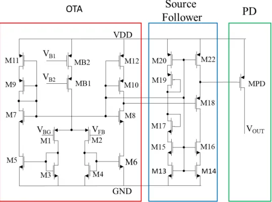
2 Circuit blocks
In this chapter we describe the design of each circuit block of the system shown in figure 10, as well as the results of the operation of each circuit, which are illustrated and analyzed. The technology that is chosen for designing the circuit blocks is the 0.35μm CMOS AMS. The process family that is used is the C35B3L3, because it provides low threshold voltage transistors. Low threshold voltage transistors have the advantage of low on-resistance and they are better for cascode configurations of the circuits in order to improve PSRR. The circuit blocks of the system are:
• Switches • Bias circuit • Comparators • Delay lines • LDO • Bandgap reference • Buffer
All circuits were simulated in typical conditions with the extracted parasitics of the physical design. Also, a corner analysis has been made for all the circuits. The corner analysis for analog design is four extreme conditions, which are the following:
• worst case speed (high temperature), where the operation of all parts is slower • worst case power (low temperature), where the operation of all parts is faster • worst case one, where PMOS transistors are slow and the NMOS are fast • worst case zero, where PMOS transistors are fast and the NMOS are slow
The high and low temperature are the limits of the range of temperatures that the application operates and they are 80oC and -20oC respectively.
2.1 Switches
The first circuit block that defines the whole architecture are the switches. Previously, it was mentioned that the S1, S2, S4, S5, S7, S8 switches are 5V low VT PMOS transistors and the rest are 5V low VT NMOS transistors.
Since, the SCs are either charged or discharged, the current that flows through the switching transistors is bi-directional, which implies that their source and their drain are swapping. Although this characteristic do not influence the layout of the design, it influences where the bulk of the switching transistor should be connected. Accordingly, there are used techniques for bulk regulation.
For the switches that include PMOS transistors it was significant to adjust their bulk voltage. Usually, the bulk of PMOS transistors is connected to the source of the transistor, which is not possible in this
15 structure. It was mandatory to find a structure for the PMOS switch that will regulate its bulk. Such a structure is introduced in [5] and is shown in figure 7. There is no possibility for bulk regulation for NMOS switches, since their bulk is connected to substrate, which has constant voltage.
The bulk regulation is achieved because the two PMOS transistors, which are connected to the bulk of the PMOS switch, are resistive transistors with long channel (W/L = 1/30). Hence, when a node is in higher voltage than the other, one of the two transistors will operate and regulate the bulk to the higher voltage.
Figure 7. Bulk regulation technique for PMOS switch.
Even though with the use of low threshold voltage transistors the on-resistance of the transistors is reduced, it is necessary to increase the width of the switching transistors and choosing their minimum channel length in order to decrease further their on-resistance. The sizes that are selected for the PMOS and NMOS switches are SP = (W/L)P = 60.000/0.5 and SN = (W/L)N = 24000/0.5 respectively. These sizes lead to an on-resistance of hundreds of mΩ in the linear region, which allows increasing the energy capacity of the SCs structure.
On the contrary, such large transistors define also the size of the chip area, with a total size of 360.000μm X 0.5μm for the PMOS switches and 62.000μm X 0.5μm for the NMOS ones. Another drawback is the increase of the gate capacitance CGS of the transistors. Such a large capacitance demands high current to be charged and discharged, which increases the power consumption during the transition.
2.2 Bias circuit
2.2.1 Bias circuit design
The bias circuit is a classic constant gm bias circuit, which is modified using cascode transistors. The cascode transistors create a stable current, which is independent from the supply voltage. This architecture is used to bias the comparators, the LDO and the buffer and it contributes to these circuits to achieve high PSRR. However, the bias circuit varies with temperature, which is not affecting significantly the biased circuits.
16
Figure 8. Bias circuit architecture.
The sizes of the transistors are shown in the table 1.
Table 1. Sizes of the elements of bias circuit.
Element Value M1 80/2 M2 120/2 M3 100/2 M4 100/2 M5 100/1 M6 100/1 M7 40/2 M8 40/2 R 10u/50u (6122 Ω)
2.2.2 Bias circuit simulation results
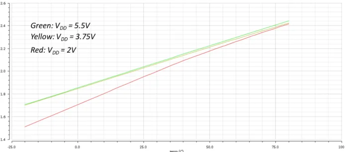
Figure 9 presents the current that is created from the bias circuit. For VDD = 5.5V and VDD = 3.75V the current has no visible difference in the full range of temperature. For around 2V supply voltage the current in low temperature deviates up to 200nA, which corresponds in a deviation of 12% of its nominal value. The currents vary from 1.5uA to 2.4uA in a temperature range of -20oC to 80oC.
17
Figure 9. Power consumption of bias circuit for different supply voltages and temperatures in typical condition.
In corner analysis the worst result appeared in worst speed case, where the deviation among the currents with different supply voltages in low temperature is 17%. Also, in this analysis there is smaller deviation in currents in high temperature.
Figure 10. Power consumption of the bias circuit for different supply voltages and temperatures in worst speed condition.
It is mandatory for the bias circuit to startup in the lowest possible supply voltage. Since the control unit must operate before the alternations in SCs configurations, the operation of the circuit for 2V supply voltage is adequate.
18
2.3 Comparators and delay lines
The control unit consists of two comparators and a delay line for each one. Each comparator must read the difference in their inputs and translate it into logic ‘1’and logic ‘0’. This logic ‘1’and logic ‘0’ is transferred through a delay line, where the signals A, B and their complementary are created.
2.3.1 Comparator design
The comparator (figure 15) is designed so that the output will drive the logic ‘1’ correctly independently of the supply voltage variations. The comparator consists of three stages and is biased from the bias circuit of figure 11.
The first stage is a classical differential amplifier, which is biased in such a way so that it will keep a stable voltage in the sources of the differential pair. The voltage reference in the differential pair is set to 400mV, which allows the desired voltage swings. The voltage difference is amplified without distortion and drives the inverter of the second stage.
The second stage consists of an inverter and an additional PMOS transistor connected between the supply voltage and the inverter. This PMOS transistor bias the inverter in the same way as the first stage. So, in the drain of this PMOS transistor the voltage is constant independent of the supply voltage and the second stage amplifies the signal and creates a first step of logic levels, where the logic ‘1’ corresponds to the value of this constant voltage. In order to restore logic signals voltages, a supplementary inverter is used.
19 In the third stage, between the transistors of the inverter a NMOS is placed, so that it prevents opposite currents, as it will be analyzed in the system. This transistor should be large so that the on-resistance will be low and will not affect the inverter.
Finally, when a change of configuration occurs, a voltage variation in reference node is transferred through the bandgap reference. This variation creates stability issues in the comparator. A compensation capacitor Cc was used to solve this problem.
The sizes of the transistors and the compensation capacitor are shown in the table 2.
Table 2. Sizes of the elements of the comparator.
Element Value M1 300/1 M2 300/1 M3 50/2 M4 50/2 MB1 100/1 MB2 60/2 M5 50/0.5 M6 1/0.5 MB3 40/2 M7 2/0.5 M8 4/0.5 M9 100/0.5 Cc 100u/165u (14.25pF)
2.3.2 Comparator simulation results
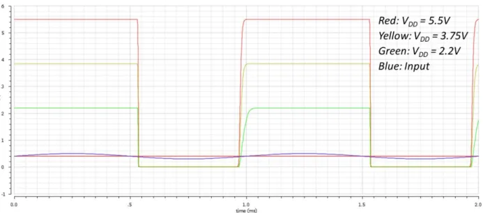
The comparator was tested using a signal of 1kHz frequency, 100mA amplitude, 400mV DC voltage with a load capacitance of 1nF.
In typical conditions and for different supply voltages the comparator is able to create the logic signals that are needed, as it is shown in figure 12.
20
Figure 12. Transient response of the comparator in the output in typical condition, when a sine at the input is applied.
Similar to bias circuit, the worst analysis was the worst speed at 80oC, illustrated in figure 13. Here the dc biasing of the circuit is changed and hence, the output cannot create the logic signals for very short periods properly. However, each change of configuration occurs only once during charging or discharging phase and eventually the logic signals will reach the desired levels.
Figure 13. Transient response of the comparator in the output in worst speed condition, when a sine at the input is applied.
2.3.3 Delay line
The delay lines that are used to lower the switching frequency are located at the output of each comparator, so that the circuits meet PSRR requirements. Also, it reduces instabilities in the system. The delay line consists of a cascade topology of three scaled inverters and four external capacitors, one at the output of the comparator and one at the output of each inverter respectively, as it shown in figure 14.
21
Figure 14. Delay line architecture.
2.4 LDO
A low dropout regulator is a circuit, which provides a constant voltage at its output, despite the load and supply voltage variations in a specific range. A typical architecture of LDO is depicted in figure 15. A LDO consists of a pass device (PD) (or pass element) and an error amplifier, which corrects any deviation in the desired output voltage. The error amplifier senses the difference of output voltage via a voltage divider and provides a feedback that regulates the pass element conductivity in order to keep the output voltage constant.
The size of the PD defines the maximum current (IOUT) that the load is capable to draw. Also, it configures the dropout voltage, which is the minimum difference between input voltage (VIN) and the output voltage (VOUT). PMOS transistors are the best option for a PD, since they are driven with low gate-to-source voltage therefore they do not need charge pump as in the case of NMOS pass elements.
Figure 15. Topology of a classic LDO.
Figure 16 shows the regions of the operation of LDO. When VIN is rising, the LDO is at off-region. After a specific level of input voltage, LDO starts operate and the output voltage increases and when the dropout input voltage is captured, the output of the LDO is stabilized at the desired output voltage. This dropout
22
voltage is the minimum input voltage which the LDO needs to operate properly. For higher voltages the LDO is in the regulation region, till a maximum input voltage.
Figure 16. Operation regions of LDO.
The efficiency of a LDO is derived from the following equation
𝑛 =𝑉𝑂𝑈𝑇𝐼𝑂𝑈𝑇 𝑉𝐼𝑁𝐼𝐼𝑁 =
𝑉𝑂𝑈𝑇𝐼𝑂𝑈𝑇
𝑉𝐼𝑁(𝐼𝑂𝑈𝑇 + 𝐼𝑄) (1)
where IQ is the quiescent current of the circuit.
If it is considered that IOUT is much higher than IQ then the efficiency depends on VOUT, VIN. However, VOUT and VIN are determined by the application and in order to achieve higher efficiency it is crucial to reduce IQ.
2.4.1 LDO design
A LDO is characterized by the following parameters: • The input voltage range that it operates. • The output voltage.
• The maximum load current. • The power that it consumes. • The PSSR.
• The line and load Regulation.
The design of the LDO is necessary to meet the specifications for the application that is opted to operate. In this application the output of the LDO is decided at 2.3V, with a maximum load current of 50mA. In the discharging phase of the SCs the supply voltage reaches 2.6V before each change of configuration, meaning that the minimum input voltage is at 2.6V. The maximum input voltage is at 5.5V, which is limited by the technology.
23 Since, the minimum input voltage is 2.6V and the output voltage is 2.3V the dropout region is 300mV. With a maximum current of 50mA, the size of the PD is chosen W/L = 10.000/0.5. The gate capacitance of the PD is 23pF.
There are many architectures for designing an error amplifier. The most common architecture is folded cascode amplifier, as in [6].An architecture independent from voltage supply with high PSRR is presented in [7], where for the first stage an OTA is used and for the second stage a compensation circuit, which also allows the large capacitance of the PD to discharge rapidly. This architecture manages to have a wide gain bandwidth and a high PSRR at the same time. The architecture also presents a quiescent current of 65μA, which represents high power consumption for a wireless autonomous system.
For the current system, the architecture that is selected uses the OTA of the first stage as in [7] and for the second stage a source follower that drives the PD. This option sacrifices the wide bandwidth of [7], increasing at the same time the PSRR and reducing substantially the quiescent current. The architecture is shown in figure 17.
The second stage is biased with the same technique that the first stage is biased, which offers the PSRR enhancement of the first stage.
Figure 17. Proposed architecture of the error amplifier of LDO with the pass device.
The reference voltage is selected at 1.22V provided by the bandgap reference circuit. In order the feedback node to meet the voltage reference the resistors in the voltage divider of the node are external and have values of 888kΩ and 1MΩ.
24
The LDO has at its output an external capacitance of 22μF that is used also for the stability of the system. This offers the option to change the capacitance depending on the maximum current that the load will draw. For example, if a load requires lower current in its active mode, then a smaller capacitance can be used at the output.
The sizes of the transistors and the pass device are shown in the table 3.
Table 3. Sizes of the elements of the LDO
Element Value Element Value
M1 20/1 M11 2/2 M2 20/1 M12 2/2 M3 2/2 M13 2/2 M4 2/2 M14 8/2 MB1 100/1 M15 2/2 MB2 60/3 M16 8/2 M5 2/2 M17 1/2 M6 2/2 M18 20/1 M7 50/2 M19 1/2 M8 50/2 M20 2/2 M9 2/2 M21 8/2 M10 2/2 MPD 10.000/0.5
2.4.2 LDO simulation results
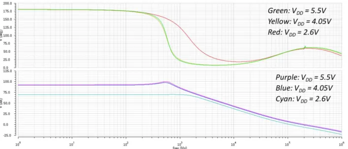
LDO is the circuit with the largest power consumption, which is almost the 50% of the consumption of the power management and the control units together. However, the power consumption is only the 30% of the power that consumes the design proposed in [7]. When VIN is minimum (2.6V) and with a quiescent current of 19.5μΑ the LDO efficiency reaches the 88.5%.
Furthermore, a higher PSRR is achieved as it reaches to -85dB in low frequencies and to -55dB in 10kHz. Also, it is achieved a low line regulation at 3.7mV/V and a low load regulation at 0.24mV/mA. The loop gain in medium-high supply voltages is 95dB and the BW is 45kHz and the PM in narrow range of frequencies drops to 15o.
In worst speed condition it is noticed that at low supply voltages the GBW is limited to 13kHz. There is a crucial point in worst zero condition (figure 22), where PM drops to 8o for and in the same range of frequencies as in typical condition. In worst one condition the circuit presents the worst PSRR and the worst line and load regulation. PSRR in low frequencies reaches the -67dB and in 10kHz the -51dB, as is shown in figure 20. The line and load regulation are high at 59.1mV/V and 3.56mV/mA respectively.
25
Table 4. Results of LDO in typical condition.
Typical Condition (27oC)
Symbol Value
Power Consumption IQ 19.5μA
Line Regulation ΔVREF/ΔVDD 3.7mV/V
Load Regulation ΔVREF/ΔIL 0.24mV/mA
Power Supply Ripple
Rejection PSRR
-85dB at 100Hz -55dB at 10kHz
Bandwidth BW 45kHz
Table 5. Results of LDO in worst power condition.
Table 6. Results of LDO in worst speed condition.
Worst Power (-20oC)
Symbol Value
Power Consumption IQ 22.5μA
Line Regulation ΔVREF/ΔVDD 0.5mV/V
Load Regulation ΔVREF/ΔIL 0.04mV/mA
Power Supply Ripple
Rejection PSRR -86dB at 100Hz -53dB at 10kHz Bandwidth BW 100kHz Worst Speed (80oC) Symbol Value
Power Consumption IQ 17μA
Line Regulation ΔVREF/ΔVDD 40.5mV/V
Load Regulation ΔVREF/ΔIL 2.4mV/mA
Power Supply Ripple
Rejection PSRR
-91dB at 100Hz -51dB at 10kHz
26
Table 7. Results of LDO in worst one condition.
Table 8. Results of LDO in worst zero condition.
Worst One (27oC)
Symbol Value
Power Consumption IQ 19.5μA
Line Regulation ΔVREF/ΔVDD 59.1mV/V
Load Regulation ΔVREF/ΔIL 3.56mV/mA
Power Supply Ripple
Rejection PSRR -67dB at 100Hz -51dB at 10kHz Bandwidth BW 100kHz Worst Zero (27oC) Symbol Value
Power Consumption IQ 21μA
Line Regulation ΔVREF/ΔVDD 3.7mV/V
Load Regulation ΔVREF/ΔIL 0.24mV/mA
Power Supply Ripple
Rejection PSRR
-84dB at 100Hz -51dB at 10kHz
27
Figure 18. Output of LDO, when supply voltage and temperature vary.
28
Figure 20. PSRR of LDO for different supply voltages in worst one condition
29
Figure 22. Gain Bandwidth and Phase Margin of LDO in worst zero.
In a LDO it is necessary to test the transient response of the circuit. Transient response shows if the output voltage converges to the desired levels, how fast this converging occurs and if there are huge fluctuations of the output voltage before the converging is about to occur.
Figure 23 presents the output voltage of the LDO in typical conditions, when changes in the load and voltage supply occur. Both supply voltage and the load current are changing level with a frequency of 100kHz. Supply voltage is changing from 2.6V to 5.5V with a period of 5ms and the load current is changing from 0 to 50mA with a period of 2.5ms. The maximum error in the output voltage is 0.25%.
In worst one condition (figure 24), when there is a change from both the load current from 0 to 50mA and the supply voltage from 5.5V to 2.6V, there is a high drop of the output voltage at 2.24V, which needs 500us to stabilize. The LDO operates with an output 60mV less than the desired output. However, the system is increasing the supply voltage, which leads eventually to the correct levels of voltage at the output.
30
Figure 23. Transient analysis of LDO when the input voltage VIN and load current ILOAD variations in typical condition.
31
2.5 Bandgap reference and Buffer
The specifications of the power management architecture and especially of the rapid voltage changes across the supercapacitors, when their configuration changes, limit the design options of the bandgap reference circuit. For this reason, it is necessary that it is selected a bandgap reference with a PSRR enhancement to eliminate the large and rapid variations in the supply voltage, caused by the reconfiguration of the SCs.
The architecture (figure 25) that is used, consists of a bandgap core circuit, an operational amplifier, a startup circuit and a PSR enhance circuit to improve the behavior of the bandgap when large variations in the supply voltage occur [8]. The unique feature of this architecture is the "PSR enhance" circuit, which drives the VG node of the bandgap core and the biasing of the operational amplifier.
It is known that the voltage reference of the bandgap reference circuit is derived by the equation
𝑉
𝑟𝑒𝑓= 𝑉
𝑏𝑒1+ 𝐼
𝑅1𝑅
2= 𝑉
𝑏𝑒1+
𝑅2
𝑅1
𝑉
𝑇ln(8)
(2)For a conventional bandgap reference the PSRR is given by the equation
𝑉
𝑟𝑒𝑓𝑉
𝑑𝑑≈ (
𝑟
𝑄1+ 𝑅
3𝑅
1)(
1 − 𝐴
𝐷𝐷𝐴
)
(3)where r
Q1is the on-resistance of the BJT and A=v
g/v
difand A
DD=v
g/v
ddthe gain and PSR of the
OpAmp respectively [8].
The PSRR can be improved by increasing the gain of the operational amplifier (OpAmp), which
causes stability issues. To avoid this case, there is another option to eliminate the second term
of the equation 3. In order to achieve this, A
DDshould be as close as possible to 1 (0dB), which
means that the output of the OpAmp follows the ripple in the power supply, and hence, the V
GS32
Figure 25. Architecture for the bandgap reference circuit proposed in [8].
2.5.1 Bandgap reference design
In the design, there are some specific points, which are mandatory to be implemented in a specific way to avoid stability issues and variations in the output and improve power consumption.
In bandgap core, it is important for M1, M2 transistors to have long channel, so that channel length modulation effect can be neglected and not affect the output of the circuit. Also, the resistors should have a high value resistance to reduce the currents. The main power consumption in this architecture is due to the bandgap core, because the transistors in OpAmp and PSR enhance blocks are working in sub-threshold region. Here, there is a tradeoff between area and power consumption, since the technology that is being used do not provide very high value resistors.
Avoiding to increase more the area, the resistors R4, R5, R6 and R7 depicted in figure 25 were not used for the design and they are replaced with a buffer and a voltage divider.
The OpAmp transistors of the differential pair should be large to improve GBW. Because of the limitations in biasing current, the GBW can be improved by increasing the transconductance of the differential pair, as the Cc has small value of 200fF. Also, there is the need to have a high gain in this block, so both the differential pair and the common source transistor M8 need to have large width.
The gain in the node VG
, A
DD is derived by the equation𝐴
𝐷𝐷=
𝑉
𝐺𝑉
𝐷𝐷=
𝑟
𝑑𝑠101/𝑔
𝑚11+ 𝑟
𝑑𝑠10 (4)33
The gain A
DDneeds to be equal to 1. So, the transistor M10 should be very resistive and M11
should have large width to increase its transconductance [8].
The final sizes of the elements of the bandgap reference that they were used for the design are
shown in table 9.
Table 9. Sizes of the elements of the bandgap reference circuit
Element Value Element Value
M1 500/2 M12 2/1 M2 500/2 M13 2/1 M3 200/1 M14 4/1 M4 200/1 M15 4/1 M5 3/3 M16 4/1 M6 3/3 Cc 16u/16u (225fF) M7 60/2 Rc 3u/135u (60kΩ) M8 50/2 C3 30u/40u (1pF) M9 60/2 R1 10u/95u (11.5kΩ) M10 1/100 R2 10u/996u (122kΩ) M11 15/1 R3 10u/996u (122kΩ)
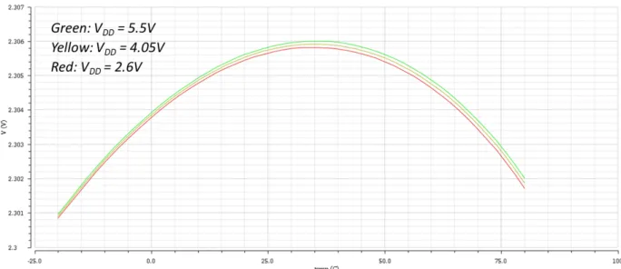
2.5.2 Bandgap reference simulation results
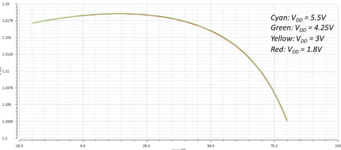
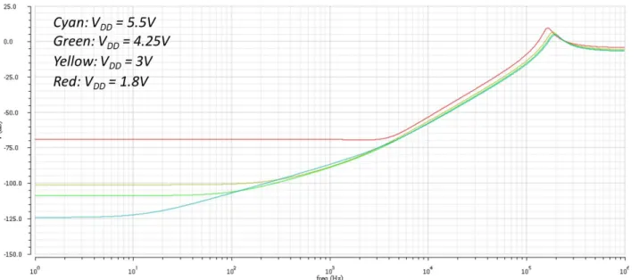
The results for the typical and for the four corners analyses are indicated in the tables 6-10. Generally, in typical conditions the power consumption of the bandgap is 10μA. An almost constant output voltage is succeeded at 1.2215V, which is changing 2.3μV/V and the temperature coefficient is 25.1ppm/oC, as is illustrated in figure 26. The PSRR in low frequencies and medium-high supply voltages is -105dB and in low supply voltages is -85dB. At 10kHz the PSRR drops to -65dB.
Power supply is not creating any differences in temperature coefficient and power consumption in all conditions.
The worst performance (figure 27) of the circuit is appeared in worst zero condition for temperature coefficient and line regulation, which are 160ppm/oC and 21.2μ/V respectively. In worst speed condition (figure 29) is noticed a drop in PSRR at low supply voltages and low frequencies, reaching of -70dB.
34
Table 10. Typical performance of the bandgap reference circuit
Typical Condition (27oC)
Symbol Value
Power Consumption IDD 10uA
Output Voltage VOUT 1.2215V
TC@(-20 ~ 80OC) ΔV
REF/ΔT 25.1ppm/oC
Line Regulation ΔVREF/ΔVDD 2.3μV/V
Power Supply Ripple
Rejection PSRR
-106dB 100Hz -63dB 10kHz
Table 11. Performance of the bandgap reference circuit in the worst power condition (low temperature)
Worst Power (-20oC)
Symbol Value
Power Consumption IDD 12.5uA
Output Voltage VOUT 1.227V
TC@(-30 ~ 90OC) ΔV
REF/ΔT 34.1ppm/oC
Line Regulation ΔVREF/ΔVDD 2.5μV/V
Power Supply Ripple
Rejection PSRR
-104dB 100Hz -66dB 10kHz
Table 12. Performance of the bandgap reference circuit in the worst speed condition (high temperature)
Worst Speed (80oC)
Symbol Value
Power Consumption IDD 8.5uA
Output Voltage VOUT 1.218V
TC@(-20 ~ 80OC) ΔV
REF/ΔT 25.8ppm/oC
Line Regulation ΔVREF/ΔVDD 17.9μV/V
Power Supply Ripple
Rejection PSRR
-107dB 100Hz -58dB 10kHz
35
Table 13. Performance of the bandgap reference circuit in the worst one condition
Table 14. Performance of the bandgap reference circuit in the worst case zero
Worst Zero (27oC)
Symbol Bandgap Reference
Power Consumption IDD 10uA
Output Voltage VOUT 1.2185V
TC@(-20 ~ 80OC) ΔV
REF/ΔT 160ppm/oC
Line Regulation ΔVREF/ΔVDD 21.2μV/V
Power Supply Ripple
Rejection PSRR
-106dB 100Hz -61.5dB 10kHz
Figure 26. Temperature dependence of the bandgap reference circuit in typical condition.
Worst One (27oC)
Symbol Value
Power Consumption IDD 10.2uA
Output Voltage VOUT 1.2185V
TC@(-20 ~ 80OC) ΔV
REF/ΔT 35.1ppm/oC
Line Regulation ΔVREF/ΔVDD 1.95μV/V
Power Supply Ripple
Rejection PSRR
-111dB 100Hz -62.5dB 10kHz
36
Figure 27. Temperature dependence of the bandgap reference circuit in worst zero condition.
37
Figure 29. PSRR result of the bandgap reference in worst speed condition.
2.5.3 Buffer design
A buffer is necessary for the system to replace the resistors that are removed from the bandgap core of the [8], which could set the voltage reference for the control unit at 400mV as it was mentioned above. Instead the voltage divider is implemented with small-size transistors and it will be analyzed in the system design.
The buffer isolates the bandgap reference circuit and the voltage divider. So, the output of the bandgap reference drives the buffer and the LDO and the buffer drives the two comparators of the control unit. The architecture of the bandgap is indicated in the figure 30.
38
Table 15. Sizes of the elements of buffer circuit
Element Value M1 50/1 M2 50/1 M3 16/2 M4 16/2 MB1 20/2 MB2 200/2
2.5.4 Buffer simulation results
The buffer like the bandgap reference has to present high PSRR, so that the output remains stable with the supply voltage variations. It is crucial for the reference in the control unit to not have significant variations and to stabilize rapidly, because otherwise it might cause stability issues in the system, while the control signals are created from the comparator.
In typical operation and low frequencies, the PSRR of the buffer is 100dB for medium-high supply voltages, and is 65dB for low supply voltages. In medium frequencies PSSR drops to 50dB, which is adequate for the system.
Figure 31. PSRR results of buffer in typical condition.
In worst one condition analysis PSSR drops to 55dB for low supply voltages, but with no significant differences.
39
40
3 System architecture and layout design
After the design of the circuit blocks the next step is to design the final system, which will meet the specification that there were set in chapter 2. The system have to be fully autonomous, generic, very low power and to operate properly in every condition. The low power consumption and the autonomy is satisfied via the design of the switches and the circuit blocks.
The system has to be also generic and to ensure its operation in every condition, which led to specific choices in the system design. A crucial part of the system is the design of the delay line, as it is responsible for the timing of the switching and the stability of the system.
Furthermore, different options were investigated for the implementation of the voltage divider that creates the threshold voltages in the comparators. Both internal and external elements were tested. The final system is illustrated in figure 33.
Figure 33. Final proposed architecture of the reconfigurable SCs system.
A physical design (layout) of the total system is implemented and it is simulated with the parasitics extracted from the layout in all conditions (post-layout simulations).
3.1 System architecture design.
The circuits described in chapter 3 are connected to form the whole system architecture depicted in figure 33. It should be noticed that each part of the system affects the operation of the whole system, since the supply voltage of each circuit is provided from the SCs bank.
41 For example, C1 is supplying all the circuits and is the input voltage of the LDO. As a consequence, each variation in the node will be transferred in all circuits. These variations are also transferred at the output of the bandgap reference, which in turn will be transferred in the control unit and power management unit. This implies that these variations must be eliminated in the control unit, as it could lead to short alternations between the logic levels. If the logic levels are not stable, stability issues would be caused in the total system, which would end up dysfunctional.
In the design the capacitors of the delay lines, the feedback and the output capacitor of LDO and the resistors that implement the voltage divider for threshold voltages are external elements. The reasons that are external will be explained with details. On the other hand, the voltage divider and a smoothing capacitor in the reference node of the comparators are internal elements in the total chip that was designed.
3.1.1 Delay capacitors
The delay capacitors are the capacitors that contribute in the configuration of the switching frequency and in the stability of the system.
First and foremost, a value has to be set for the four capacitors that are at the nodes, where the signals A, B and their complementary are created. These capacitors need to set the system in a frequency that the total system will operate correctly. This frequency is derived from two specifications:
• The maximum frequency that all the circuits can operate with a high PSRR.
• The minimum frequency that the switching will not cause unbalances and more power consumption in the system.
Generally, the high switching frequency decreases the power consumption because when changes among the configurations occur, very high currents that reaches one or two amperes are moving among the SCs to cover the large voltage difference that they preserved from the previous state. These currents are creating consumption in the switches and the faster switching frequency decreases this.
However, there is an upper limit of the frequency for the system to be possible to operate. This limit is set from the PSRR bandwidth of the circuits. For this reason the switching frequency is set to 10kHz. The frequency of 10kHz is a medium frequency, which requires external capacitors in the delay chain. Therefore, the third and fourth external capacitors of the chain are 30nF and together with the inverters set the correct frequency in the signals.
Stability issues.
The first capacitor in the delay chain is set to 22μF, which is a significantly large value compared to the other four capacitors. This value is derived from the response of the system while it is charging. The reason is that the logic signals at the output of the comparators have to delay till the comparators inputs are able to detect a difference, before they drive the signals to the switches.
42
This choice led to the additional NMOS transistor in the third stage of the comparators (figure 11), as the large capacitance preserve the voltage in the node for long time and when there is a transition between configurations, opposite currents were driven through the PMOS transistor of the inverter to the system. Analytically, it was mentioned above that the variation, when there is an alternation in configurations, causes to the voltage reference ripples, which leads the comparators to not be able to keep the logic signals. So, before an alternation happens, the comparators are gathering a difference in their input signals, that even the ripples are not able to affect the output logic signal.
Because, the first capacitance is huge, the second capacitance in the chain is set at 10nF.If it is more, then the delay becomes so long that the threshold voltages cannot be set properly for both charging and discharging.
3.1.2 Voltage divider for threshold voltages
The first attempt in the design of the voltage divider to configure the right thresholds for the comparators, considered that these dividers must be on-chip. For this attempt there were three choices:
• Resistors that are available in the technology.
• Transistors, like there are at the output of the buffer.
• Capacitors or transistors that will be used as capacitors to implement a voltage divider.
The resistors that exist in the technology are not having large sheet resistance values. They should either have a huge size or small resistance, which are both problematic in the design. The first option covers a huge area in the design of the chip and the second option draws a lot of current from the feedback node at the fourth SC and hence it reduces the energy efficiency and causes stability problems.
The second and third choices were impossible to be implemented, as the voltage varies from 0 to 5.5V, affecting the thresholds’ levels at the inputs of the comparators.
So, the other alternative is the use of external resistors. The external resistors can be from hundreds of kΩ to a few ΜΩ, decreasing the current drawn from the fourth capacitor. Also, this solution offers the ability of the system to be generic, as it gives flexibility to the system, when other load and other input charging voltage and current are used.
3.1.3 Reference node of comparators
On the contrary to the option that is used for voltage divider to produce the threshold voltages, for the reference node of the comparators are used internal resistors and a smoothing capacitor.
This ability came from the buffer because it produces a constant voltage output close to the output voltage of the bandgap, which is not affected from the current that flows at the output. So, with a constant voltage two normal PMOS transistors are used with specific sizes that are generating 400mV at the inputs of both comparators.
43 The smoothing capacitor is used to eliminate most of the variations that are transferred from the bandgap and the buffer due to voltage changes in their supplies. This smoothing capacitor and the capacitor at the output of each comparator ensure the stability of the system.
3.2 Physical design (layout)
The physical design of the chip is the last step of the chip design. Layout techniques are considered, where possible mismatches, noise and technology variations are reduced. Such techniques are the common centroid technique, the use of dummy devices, guard rings and others.
In the physical design, specific rules have to be followed that are derived from the documentation of the technology and finally the whole layout must be free of Design Rules Check (DRC) errors. Also, a Layer vs Schematic (LVS) confirmation is necessary that ensures that the connections in the schematic design, namely the architecture design that was implemented, are the same with the connections created in the physical design.
After that a post-layout simulation have to be done with the extracted parasitics of each structure and device. The parasitics are various capacitances that are created between two layers and resistance dependes on the resistivity that each layer has.
The total chip is depicted in figure 34, where at upper part the switches and their interconnections are located and in the lower part there are the control and power management unit.
44
3.2.1 Switch Interconnections
It is known that each layer is possible to withstand a specific density of current. If that density is surpassed, then the layer could be destroyed or degraded. This issue must be taken into account, since during the switching large currents for short period are flowing through the power transistors and eventually the metals that connect them. These large currents are reaching a peak of 2A for 200μs.
However, this significantly large currents are for a short period and they are not affecting the layer with the same weight as a DC current. For AC current it can be used the equation 5.
𝐽𝑝𝑒𝑎𝑘_𝑎𝑐 =2 × 10
6
√𝐷𝐶 (5)
In the equation 5, Jpeak_ac represents the peak density that the current has, and the DC represents the duty cycle of the period that the AC current has.
In this architecture, a change is occurring only once for each configuration for both charging and discharging. So, there is not a DC that it can be taken into account. For this reason, the DC is selected 0.1, which is a very low value that is close to the reality. So, the metals in the physical connections of the switches have to be at least 200um width.
The flavor of the technology the C35B3L3 offers a three metal option. So, metal 2 and metal 3 are used stacked with a size of 100um width. For metals with such large width, it is mandatory to create slots inside them, as it is shown in figure 35, where a huge part of metal 3 with slots is depicted.
Figure 35. Metal slots in metal 3 layer for a large metal width interconnection
3.2.2 Matching techniques.
The most common techniques to eliminate various problems in the chip or the construction of the wafer are presented in figure 36.
The first technique is common centroid, the second technique is matching and the third technique is the use of guard rings. There is also a technique similar to common centroid that is called interdigitated.
45
Figure 36. (a) Common centroid technique. (b) Symmetry. (c) Guard rings [9].
Common centroid
Most of the circuits have a differential amplifier with an active load, where the transistors must behave in the same way. When a wafer is constructed, there are variations in temperature, doping etc. from one side to the other. This variation might cause to transistors a slight difference in parameters, which can be translated to a slightly different operation of the transistors.
The solution to this problem is the common centroid technique, where the devices are split in two, four or more parallel parts and are placed in such a way, which will force the transistors to have the same variations. In figure 37 is shown a use of the common centroid technique in the physical design. The transistors belong to the differential pairs of the OTA amplifier of the LDO.
Figure 37. Implementation of differential pair using common centroid technique.
An example of interdigitated transistors is illustrated in figure 38, where the resistors A and B with the same size that implement the bandgap core, are split in 6 parts and they are placed one after another.
46
Figure 38. Integiditated technique for the symmetric resistance of bandgap core.
Dummy Devices
Matching techniques are also used in the physical design. Generally, the design must be as symmetric as possible to avoid huge variations. Another issue is that when a layer is constructed it must be designed in such a way that it will not have mismatches in the edges of the block. In figure 39 and 40 are notified the dummy devices in layer poly and layer poly 2 respectively. Transistors with fingers require dummy poly structures in both sides.
47
Guard Rings
Finally, guard rings are used for sensitive circuits in order to avoid electromagnetic interference from metals that flow large currents. Also, the noise from the substrate and leakage currents in the substrate are reduced. For example, bandgap core is a sensitive circuit and it needs protection from the large currents that flow through the switches and through the PD of the LDO (figure 40).
Guard rings are implemented connecting multiple vias with the substrate, which circles the sensitive circuit blocks that they must be protected.
Figure 40. Guard ring around the bandgap core, which is a sensitive circuit.
3.2.3 System simulation
The designed chip was simulated with the extracted parasitics, as it was mentioned previously. The post-layout simulation happened for 700μA minimum charging current and 15mA maximum charging current. For discharging the currents that were selected are 2μA and 50mA, minimum and maximum respectively. The power management and control unit demand together 45μA and when the supply voltage is 5.5V they consume 248μW. The average consumption in the switches, when the discharging current is maximum (50mA) is 480μW.
Charging
The system was simulated for 700μΑ and 15mA charging currents, which is the charging current range of the system. In both limits the system operates properly and it is compared with a fixed 400mF capacitor. In the case of 700μΑ current the system needs 2464s to charge to 5.5V (figure 41), on contrary to the fixed
48
capacitor, which needs 3337s to be fully charged. In the case of 15mA current the system requires 101s to charge, while the fixed capacitor needs 147s (figure 42).
Figure 41. The charging of the system for 700μΑ current compared with a fixed 400mF capacitor.
Figure 42. The charging of the system for 15mΑ current compared with a fixed 400mF capacitor.
In figure 43 is presented the worst speed condition analysis for charging current 700μΑ. Here the system needs 104s to charge and still manages to alter the configurations properly.
49
Figure 43. Worst speed condition analysis for charging current 700μΑ.
In figure 44 is presented the worst zero condition analysis for charging current 15mA. As it can be seen the system oscillates for a short period during the transition from SP to the AP configuration.
The oscillation occurs because the logic signals of the comparators are reversed, as there is a ripple in reference input of the comparators, as it is analyzed above.
![Figure 3. Charging phase of the SCs structured compared with fixed C/4 and fixed C*4 capacitors [2]](https://thumb-eu.123doks.com/thumbv2/123doknet/15036155.690245/11.918.266.659.263.515/figure-charging-phase-structured-compared-fixed-fixed-capacitors.webp)