HAL Id: hal-01139277
https://hal.archives-ouvertes.fr/hal-01139277
Submitted on 3 Apr 2015
HAL is a multi-disciplinary open access
archive for the deposit and dissemination of
sci-entific research documents, whether they are
pub-lished or not. The documents may come from
teaching and research institutions in France or
abroad, or from public or private research centers.
L’archive ouverte pluridisciplinaire HAL, est
destinée au dépôt et à la diffusion de documents
scientifiques de niveau recherche, publiés ou non,
émanant des établissements d’enseignement et de
recherche français ou étrangers, des laboratoires
publics ou privés.
New Si-based multilayers for solar cell applications
Ramesh Pratibha Nalini, Christian Dufour, Julien Cardin, Fabrice Gourbilleau
To cite this version:
Ramesh Pratibha Nalini, Christian Dufour, Julien Cardin, Fabrice Gourbilleau. New Si-based
mul-tilayers for solar cell applications. Nanoscale Research Letters, SpringerOpen, 2011, 6 (156), pp.1-5.
�10.1186/1556-276X-6-156�. �hal-01139277�
N A N O E X P R E S S
Open Access
New Si-based multilayers for solar cell applications
R. Pratibha Nalini, Christian Dufour, Julien Cardin, Fabrice Gourbilleau
*Abstract
In this article, we have fabricated and studied a new multilayer structure Si-SiO2/SiNxby reactive magnetron
sputtering. The comparison between SiO2 and SiNxhost matrices in the optical properties of the multilayers is
detailed. Structural analysis was made on the multilayer structures using Fourier transform infrared spectroscopy. The effect of specific annealing treatments on the optical properties is studied and we report a higher visible luminescence with a control over the thermal budget when SiO2is replaced by the SiNxmatrix. The latter seems
to be a potential candidate to replace the most sought SiO2 host matrix.
Introduction
The third generation of solar cells aims at reducing the cost and at improving the efficiency. Thin film solar cells based on silicon nanostructures is one of the most researched system to achieve such a target [1-3]. Ever since the discovery of the visible luminescence of the porous Si by Canham [4] various research groups have exploited the room temperature photoluminescent nat-ure of silicon by fabricating different kinds of Si-based nanostructures. The luminescence is attributed to the quantum confinement of carrier in Si-nanoclusters (Si-nc) [5-8]. Among the methods of obtaining the Si nanostructures we cite electrochemical etching [4,9], fabrication of silicon dots by plasma sputtering techni-que [10], and multilayer approach [8,11,12].
The important part of the ongoing research involves Si-nc embedded in an amorphous matrix such as SiO2,
SiNx, or amorphous silicon. Though Si-nc embedded in
SiO2is the most common structure, the problem of
car-rier injection in this matrix comes as a major drawback owing to the large band gap of SiO2. Hence the
replace-ment of SiO2 by other dielectric matrices with smaller
bandgap turns out to be a solution. SiNxmatrix meets up these requirements and hence Si-nc embedded in SiNx matrix has become a material of choice in the recent past. In this article, we develop a new multilayer composition silicon-rich silicon oxide (SRSO)/SiNx to overcome the insulating nature of SiO2 by taking
advan-tage of the reduced bandgap in SiNx. Using SiNx as the host matrix favors the electrical conductivity of carriers
while we still maintain the quantum confinement as done with the SiO2 matrix. This study aims at
fabricat-ing and comparfabricat-ing the light emission properties of three different kinds of multilayer compositions: (a) SRSO/ SiO2, (b) SRSO/SiNx, (c) SiNx/SiO2. Such a study is
important to understand the influence of host matrices on the Si-nc and consequently to achieve an optimized solar cell device in the future.
Experimental details
Three kinds of multilayer structures were fabricated on 2” Si wafer by reactive magnetron sputtering comprising 50 patterns of SRSO/SiO2, SRSO/SiNx, and SiNx/SiO2.
We define the gas flow rate asrg=fg/(fg +fAr) where fg
represents the N or H2gas flow and fAr represents the
Argon gas flow. The SiO2 sublayer was fabricated by
sputtering the SiO2 cathode under pure Ar plasma.
Reactive magnetron sputtering, an approach developed by our team, was used for the fabrication of SRSO sub-layers. It takes advantage of the oxygen reducing capa-city of hydrogen when introduced into the Ar plasma [8]. The hydrogen-rich plasma favors Si excess in the SiO2 sublayer. Besides this in order to facilitate a higher
incorporation of Si in the matrix, both SiO2and Si
cath-odes were used to fabricate the SRSO sublayer. The powers of SiO2 and Si were maintained as 7.4 and 2.2
W/cm2, respectively. The hydrogen rate rH was
main-tained at 50% while the total flow fg +fArwas fixed at
10 sccm. The pressure in the chamber was chosen as 3 mTorr. Thus the SRSO/SiO2 multilayer structure was
deposited by an alternative reactive sputtering under hydrogen-rich plasma for the SRSO layer and pure Ar plasma for the SiO2 sublayer. The SiNx layer was
* Correspondence: fabrice.gourbilleau@ensicaen.fr
CIMAP UMR CNRS/CEA/ENSICAEN/UCBN, 6 Bd. Maréchal Juin, 14050 Caen Cedex 4, France
© 2011 Nalini et al; licensee Springer. This is an Open Access article distributed under the terms of the Creative Commons Attribution License (http://creativecommons.org/licenses/by/2.0), which permits unrestricted use, distribution, and reproduction in any medium, provided the original work is properly cited.
fabricated by sputtering the Si cathode and simulta-neously introducing nitrogen into the Ar plasma. The nitrogen rate rN was kept at 10% while the total flow
rate was fixed at 10 sccm. The pressure in the chamber was chosen as 2 mTorr for SiNxlayers. The temperature
of deposition was maintained at 500°C for all the cases. The thickness of the SRSO sublayer was fixed to be 3.5 nm in order to be within the quantum confinement regime. In order to understand the influence of SiNx matrix, two different thicknesses of the SiNx sublayer
(3.5 and 5 nm) were chosen.
The FTIR spectra of these samples were recorded in absorption configuration using Nicolet Nexus spectro-meter at Brewster’s angle (65°). The photoluminescence (PL) spectra of the annealed samples were obtained in the visible range using Jobin Yvon monochromator in the wavelength range 550-1100 nm. The excitation wavelength of 488 nm (Ar laser) was used for measurements.
Results and discussions FTIR spectroscopy
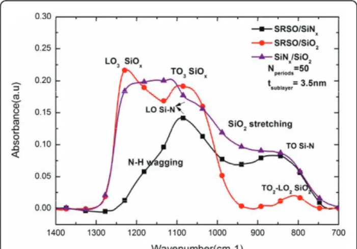
Figure 1 shows the FTIR spectra obtained for the non-annealed SRSO/SiO2, SiNx/SiO2, and SRSO/SiNx
multi-layers. The spectra were recorded at the Brewster angle of 65° that enables the detection of the LO3 mode of
silica at about 1250 cm-1in addition to the TO3 mode
located near 1080 cm-1.
In SRSO/SiO2 around 1225 and 1080 cm-1we notice
the LO3 and TO3 peak from the Si-O stretching, the
TO4-LO4 doublet between the 1100-1200 cm-1and the
TO2-LO2 asymmetric stretching of Si-O from SiO2 at
810 and 820 cm-1, respectively [13]. The presence of Si-nc is attested by the intensity of the LO3 peak which is
representative of the Si-O bond at the interface [14]
between silicon and silica while the TO3 vibration mode
at about 1080 cm-1is the signature of the volumic silica. The SiNx/SiO2film has a broad peak in the 1250-950
cm-1region which can be due to the contributions of both LO and TO modes from SiO2 and Si-N stretching
mode [15-17]. The absorption band located around 860 cm-1could be attributed to the Si-N asymmetric stretch-ing mode.
In the case of SRSO/SiNx films, the shoulder around 1190 cm-1may be due either to N-H bond [16,18] or to a contribution of the LO3 mode of Si-O-Si bonds at
180° [13]. Such a result is the signature of the Si nano-particles formation within either the SiNx [19] and/or
the SRSO sublayer [13]. Between 1050 and 1070 cm-1 lies the LO peak of a-SixNyHzfrom Si-N as it has been
observed in the SiNx/SiO2 spectrum adding the
contri-bution of the TO Si-O mode. PL spectra
The PL emission spectra of the annealed multilayer structures were measured using 488 nm excitation wavelength and the spectrum was recorded in the visible range. Two different annealing treatments were chosen for the study–1 min-1000°C (rapid thermal annealing– RTA) and 1 h-1100°C under N2 atmosphere, the latter
being the classical annealing treatment used for recover-ing defects in SiO2 matrix to favor luminescence from
Si-nc [3]. Figure 2 shows the effect of the annealing treatment on the PL intensity of the three kinds of mul-tilayer structures. All the curves are normalized to a total thickness of 100 nm. Since the number of periods and the sublayer thickness remains the same for each of these films, i.e., Nperiods(tsublayer1/tsublayer2) = 50(3.5/3.5
nm), it becomes possible to make a comparative analysis from the PL spectrum of these three different multilayer structures. The interference effect in PL intensity has been investigated by the method proposed by Holm et al. [19] for all the spectra presented in this article. This method gives us the PL intensity versus layer and sub-strate parameters (refractive indices, thicknesses). We assume and homogenous density of emitting centers, an average refractive index within the thickness of multi-layer. For measurements on Figure 2 no important change in PL has been found due to interference.
It can be noticed from the spectrum that when the multilayers are subjected to the classical annealing treat-ment of 1 h-1100°C, there is no emission from the SRSO/SiNx while the SRSO/SiO2 structure shows a
strong PL signal and has a wide range of emission spec-trum. At the same time, it is interesting to note a very weak PL signal in the case of SiNx/SiO2. The PL peaks
appear in a region usually related to the optical transi-tions in the SiO2 matrix due to the presence of defects
[3,17]. The lower part of Figure 2 shows the PL
Figure 1 FTIR spectra of the multilayer structures at Brewster’s angle.
Naliniet al. Nanoscale Research Letters 2011, 6:156 http://www.nanoscalereslett.com/content/6/1/156
spectrum recorded after annealing the multilayer struc-tures for 1 min at 1000°C (RTA). The response of the multilayers to this annealing treatment shows almost a reversed trend of what was observed in the case of clas-sical annealing treatment. It can be noted that the SRSO/SiNx has the highest intensity. No PL emission has been recorded from the SRSO/SiO2 system. We
may note from the figures that the luminescence peak arising from the SiNx/SiO2 structure around 1.9 eV is
the same whatever the annealing temperature. The fit-ting of the PL curve recorded from the SRSO/SiNxfilm evidences the presence of two emission bands centered at 1.65 and 1.37 eV. Though this result is interesting and shows the possibility of exploiting SRSO alternated with the SiNx sublayer to achieve a control over the
thermal budget, it also has to be mentioned that the PL intensity obtained is one order of magnitude lower than the emission of SRSO/SiO2subjected to classical
anneal-ing. Hence, two methods of fabrication were attempted with the aim of increasing the PL intensity: (i) increasing the SiNx sublayer thickness to 5 nm and (ii) doubling the number of periods, i.e., fabricating 100 periods of 3.5 nm SRSO alternated with 5 nm SiNx. Figure 3
shows the effect of the aforesaid fabrication methods on the PL spectrum of the SRSO/SiNxmultilayers. All the
spectra have been normalized to 100 nm thickness for comparison. The interference effect in PL intensity has been also investigated by the previously mentioned method PL intensity from both 50 periods multilayers should be decreased by about 15%, in order to take into account the enhancement effect due to maxima of inter-ference. The first method adopted reveals that the SiNx thickness has some significant contribution toward the luminescence. There is a slight change in the emission wavelength from 1.59 eV with 3.5 nm SiNx sublayer to 1.55 eV in the case of 5 nm SiNx sublayer. Irrespective
of the number of periods deposited, for a given sublayer thickness the wavelength of emission peak remained constant. It is interesting to note that the emission intensity increases with the SiNxthickness. This result
motivated toward trying out the second method men-tioned and it can be noticed that the PL signal increases 7.4 times when the number of (3.5 nm)SRSO/(5 nm) SiNx pattern is increased from 50 to 100. For that case one can notice is the presence of a small peak between 1.90 and 1.65 eV and another one around 1.5 eV. The inset in Figure 3 shows a comparison between the SRSO/SiO2 annealed at 1 h-1100°C and SRSO/SiNx
structure subjected to RTA. One can notice that the emission peak from the SRSO/SiNx system shifts in the visible region and this is one of the advantageous aspects for the solar cell application. It is very interest-ing to note that the SRSO/SiNx annealed for a very
short time of 1 min at 1000°C is 1.43 times more intense than the SRSO/SiO2 structure annealed for a
Figure 2 Effect of annealing treatment on the PL intensity of the multilayer structures.
Figure 3 Effect of sublayer thickness and total thickness of SiNxon the PL spectrum on RTA. (Inset: comparison between the SRSO/SiO2annealed at 1 h-1100°C and SRSO/SiNxstructure
long time of 1 h and at higher temperature. Accounting for the interference effect, we can infer that SRSO/SiNx
exhibits higher PL intensity than SRSO/SiO2. Thus, it
can be seen that a replacement of the SiO2 sublayer by
the SiNx sublayer and alternating it with the SRSO
sub-layer not only favors luminescence but paves way to achieve a control over the thermal budget.
Discussion
The PL spectra of the SRSO/SiNxsubjected to two dif-ferent annealing treatments show that the quenching of the PL signal after an RTA can be attributed to the non-radiative defects either at the interface of Si-nc and the SiO2 matrix or within the SiO2 matrix itself which
traps the photon arising from the recombination of the exciton within the Si-nc. On the contrary, it can be seen that the SiNx sublayer favors luminescence even if this
later could be attributed to the defects in the matrix. Noticing the shift in emission peak from 1.9 to 1.6 eV in the case of SiNx/SiO2 and SRSO/SiNx, respectively, it
can be said that the sandwiching of SRSO between SiNx instead of SiO2 sublayers not only favors luminescence
but also exhibits luminescence in a region attributed to the emission from Si-nc. This implies that though at this temperature SiNx shows a defect-related PL, when alternated with SRSO, the emission from Si-nc becomes dominant.
On the other hand, the quenching of PL in classically annealed SRSO/SiNx is quite surprising as several
authors have noticed an increase of the PL signal either from SRSO or SiNx after such annealing. It also should
be noted that the‘SRSO sublayer’ fabricated under the same conditions and alternated with SiO2 sublayer has a
high emission. Hence one can conclude that the pre-sence of the SiNxsublayer quenches the PL. This can be attributed either to the coalescence of Si clusters at such an annealing treatment thereby overcoming the quan-tum confinement regime or to the non-radiative defects at the interface between SRSO and SiNxor in SiNx. The increase of the PL emission when increasing the number of layer could be the result of H diffusion during the deposition process which favors the recovering of the defects and the Si nanoparticles formation. Such a hypothesis is supported by the presence of N-H bonds revealed by FTIR experiments in the non-annealed mul-tilayers and that can be attributed to the Si-nc formation [17]. Another explanation could be the increase of strain with the number of layer that favors the Si-np formation resulting in an increase of the Si-np density and hence in the PL emission. However, the comparison in the inset of Figure 3 of the two types of multilayers demon-strates the advantage to replace the SiO2sublayer by the
SiNx. HRTEM experiments are in progress to under-stand the optical behavior of these multilayers.
Conclusion
The multilayers were fabricated using the sputtering technique and the FTIR spectrum revealed its character-istic peaks. Although SiO2 is the most sought host
matrix, we evidenced the interest of replacing it with the SiNx matrix. A higher intensity of PL emission was
obtained for RTA when SiNxmatrix was used whereas
from the SiO2 matrix there was no considerable
inten-sity at such an annealing treatment. We have achieved comparable intensity of emission within one minute of annealing and at a lesser temperature, in comparison to the classical annealing treatment that is done for longer time and slightly higher temperature. We also observe an increase in the PL emission with increase in the number of periods. High-resolution electron microscopy experiments are in progress to understand the effect of the annealing process on the achieved optical properties. This set of above-mentioned results paves the way for the fabrication of novel structures for solar cell device applications similar to the one recently reported by Di et al. [20].
Abbreviations
PL: photoluminescence; RTA: rapid thermal annealing; Si-nc: Si-nanoclusters; SRSO: silicon-rich silicon oxide.
Acknowledgements
This study is supported by the DGA (Defense Procurement Agency) through the research program no. 2008.34.0031.
Authors’ contributions
RPN fabricated the multilayers under investigation and carried out the characterization studies.CD and JC made significant contribution to the optical properties and interference effect. FG conceived of the study and participated in the coordination and writing of the manuscript. All authors read and approved the final manuscript.
Competing interests
The authors declare that they have no competing interests. Received: 24 September 2010 Accepted: 18 February 2011 Published: 18 February 2011
References
1. Conibeer G, Green M, Corkish R, Cho Y, Cho EC, Jiang CW, Fangsuwannarak T, Pink E, Huang Y, Puzzer T, Trupke T, Richards B, Shalav A, Lin KL:“Silicon nanostructures for third generation photovoltaic solar cells”. Thin Solid Films 2006, 511-512:6542.
2. Conibeer G, Green M, Cho EC, Konig D, Cho D, Fangsuwannarak T, Scadera G, Pink E, Huang Y, Puzzer T, Huang S, Song D, Flynn C, Park S, Hao X, Mansfield D:“Silicon quantum dot nanostructures for tandem photovoltaic cells”. Thin Solid Films 2008, 516:6748.
3. Gourbilleau F, Ternon C, Maestre D, Palais O, Dufour C:“ Silicon-rich SiO2/
SiO2multilayers: A promising material for the third generation of solar
cell”. J Appl Phys 2009, 106:013501.
4. Canham LT:“ Silicon quantum wire array fabrication by
electrochemical and chemical dissolution of wafers”. Appl Phys Lett 1990, 57:1046-1048.
5. Wolkin MV, Jorne J, Fauchet PM, Allan G, Delerue C:“Electronic states and luminescence in porous silicon quantum dots: the role of oxygen”. Phys Rev Lett 1999, 82:197.
6. Puzder A, Williamson AJ, Grossman JC, Galli G:“Surface control of optical properties in silicon nanoclusters”. J Chem Phys 2002, 117:6721. Naliniet al. Nanoscale Research Letters 2011, 6:156
http://www.nanoscalereslett.com/content/6/1/156
7. Tan WK, Yu MB, Chen Q, Ye JD, Lo GQ, Kwong DL:“Red light emission from controlled multilayer stack comprising of thin amorphous silicon and silicon nitride layers”. Appl Phys Lett 2007, 90:221103.
8. Gourbilleau F, Portier X, Ternon C, Voivenel P, Madelon R, Rizk R:“Si rich/ SiO2nanostructured multilayers by reactive magnetron sputtering”. Appl
Phys Lett 2001, 78:3058.
9. Von Behren J, Van Buuren T, Zacharias M, Chimowitz EH, Fauchet PM: “Quantum confinement in nanoscale silicon: The correlation of size with bandgap and luminescence”. Solid State Commun 1998, 105:317. 10. Furukawa S, Miyasato T:“Quantum size effects on the optical bandgap of
microcrystalline Si:H”. Phys Rev B 1988, 38:5726.
11. Lockwood DJ, Lu ZH, Baribeau JM:“Quantum confined luminescence in Si/SiO2superlattices”. Phys Rev Lett 1996, 76:539.
12. Zacharias M, Heitmann J, Scholz R, Kahler U, Schmidt M, Bläsing J:“Size controlled highly luminescent silicon nanocrystals: A SiO/SiO2
superlattice approach”. Appl Phys Lett 2002, 80:661.
13. Ternon C, Gourbilleau F, Portier X, Voivenel P, Dufour C:“An original approach for the fabrication of Si/SiO2multilayers using reactive
magnetron sputrering”. Thin Solid Films 2002, 419:5.
14. Olsen JE, Shimura F:“Infra-red reflection sprectroscopy of the SiO2-silicon
interface”. J Appl Phys 1989, 66:1353.
15. Dupont G, Caquineau H, Despax B, Berjoan R, Dollet A:“Structural properties of N rich a-Si-N:H films with a low electron trapping rate”. J Phys D Appl Phys 1997, 30:1064.
16. Scardera G, Puzzer T, Conibeer G, Green MA:“fourier transform infrared spectroscopy of annealed silicon rich silicon nitride thin films”. J Appl Phys 2008, 104:104310.
17. Delachat F, Carrada M, Ferblantier G, Grob JJ, Slaoui A, Rinnert H:“The structural and optical properties of SiO2/Si rich SiNxSi-ncs”.
Nanotechnology 2009, 20:275608.
18. Bae S, Farber DG, Fonash SJ:“Characteristics of low temperature silicon nitride (SiNx:H) using electron cyclotron resonance plasma”. Solid State
Electron 2000, 44:1355.
19. Holm RT, McKnight SW, Palik ED:“Interference effects in luminescence studies of thin films”. Appl Opt 1982, 21:2512.
20. Di D, Perez-Wurfl I, Conibeer G, Green MA:“Formation and
photoluminescence of Si quantum dots in SiO2/Si3N4hybrid matrix for
all Si tandem solar cells”. Sol Energy Mater Sol Cells 2010, 94:2238.
doi:10.1186/1556-276X-6-156
Cite this article as: Nalini et al.: New Si-based multilayers for solar cell applications. Nanoscale Research Letters 2011 6:156.
Submit your manuscript to a
journal and benefi t from:
7 Convenient online submission 7 Rigorous peer review7 Immediate publication on acceptance 7 Open access: articles freely available online 7 High visibility within the fi eld
7 Retaining the copyright to your article