The Development of Components for Ultrafast
All-Optical Communication Networks
Elisabeth Marley Koontz
B.S., Electrical Engineering
Southern Methodist University (1994)
S.M., Electrical Engineering and Computer Science
Massachusetts Institute of Technology (1996)
Submitted to the
Department of Electrical Engineering and Computer Science
in partial fulfillment of the requirements for the degree of
Doctor of Philosophy in Electrical Engineering
at the
MASSACHUSETTS INSTITUTE OF TECHNOLOGY
June 2000
@ 2000 Massachusetts Institute of Technology
All Rights Reserved.
ENG
MASSACHUSETTS INSTITUTE OF TECHNOLOWJUN 2 2 20
LIBRARIES
Author
E abeth Marley Koontz
11 May 2000
Certified by
*1 Y'
Leslie A. Kolodziej ski
Professpr-
9f Electrical Engineering
T
Accepted by
hur C. Smith
Chair, Department Committee on Graduate Students
Department of Electrical Engineering and Computer Science
The Development of Components for Ultrafast All-Optical
Communication Networks
by
Elisabeth Marley Koontz
Submitted to the Department of Electrical Engineering and Computer Science on 11 May 2000, in partial fulfillment of the
requirement for the degree of
Doctor of Philosophy in Electrical Engineering
Abstract
The need for ultrafast (greater than 100 Gbps) all-optical communication networks is amplified as the amount of data-containing communication traffic continues to grow at an exorbitant rate. Multiplexing schemes are attractive, as they enable increased transmission over silica fiber already buried and in use. One of the key components enabling Wavelength Division Multiplexed (WDM) propagation is the distributed feedback (DFB) laser. A periodic index modulation, typically buried within the device structure (hence requiring an overgrowth step), is used to select the specific operating wavelength of the laser. As the WDM wavelength spacing continues to decrease, the increasing demands placed on the fabrication of the DFB lasers bring the fabrication issues to the forefront. Similar patterned surface overgrowth issues need to be addressed for realization of wavelength-selective filters, e.g. Bragg-resonant filters, for all-optical routing. Issues pertaining to the formation of buried index contrasts, for application to future WDM network components, are addressed.
Of importance to Time Division Multiplexed (TDM)-based propagation schemes is the
multiplexing and demultiplexing of the ultrafast data streams. All-optical switching as well as optical (de)multiplexing are very attractive alternatives to optoelectronic conversion. Many optical switching schemes require the use of a semiconductor optical amplifier (SOA) as the nonlinear medium, as well as optical clock sources with repetition rates on the order of GHz (for integration with electronic components). For TDM network propagation rates on the order of Tbps, lasers must be capable of producing pulses shorter than a picosecond. Mode-locking of laser cavities is an attractive method of ultrashort pulse generation. A semiconductor saturable absorber mirror is a monolithically integrated device utilized for passive mode-locking of a wide variety of lasers. The development of SOAs as well as semiconductor saturable absorber mirrors is discussed.
Thesis Supervisor: Leslie A. Kolodziejski Title: Professor of Electrical Engineering
Acknowledgements
The Massachusetts Institute of Technology is a unique institution. Time spent at MIT is generally conducted with one's head down, running full steam ahead, and looking up only occasionally to glimpse at the world outside. It is a place full of dichotomies; a place in which everyone is confident, yet everyone is intimidated. A place in which everyone is smart, yet never as smart as their colleague. A place in which everyone learns an enormous amount in very short period of time, yet it is not enough. The pursuit of a degree at MIT is also a dichotomy. The rewards are great upon leaving The Institution, however the arduous road to graduation will forever be ingrained in one's memory.
My time spent at MIT has been bittersweet at best. Were it not for the following individuals, my
experience would have been much more bitter than sweet.
To Prof. Leslie A. Kolodziejski, I am eternally grateful. Thank you for giving me the opportunity to pursue my Ph.D. in your laboratory; were it not for you, I would not have made it through this place. You are an amazing individual, a fabulous advisor and boss, and most of all a wonderful friend. Please know that all you have endured has made you an amazing mentor, one that I can only hope to duplicate. Thank you for sharing your wisdom and experiences with me; you have taught me more than I could ever have hoped for!
To Dr. Gale S. Petrich, I can not thank you enough. We have learned a great deal from one another, and persevered though times that have made us both better people. Thank you for all of the time you invested in me with regard to the laboratory; you are a very wise man in the world of engineering. Thank you for all of the time you spent writing the many Matlab scripts for x-ray data and miscibility gap graphing. Thank you also for being a sounding board for x-ray discussions, and for your assistance with the interpretation of those equation things.
To Erik R. Thoen, you are a GREAT pal. Thank you for being a wonderful colleague; it has been a pleasure to work with you. You have taught me a lot, even though you're a "young punk". Thanks also for being a sounding board -we're finally allowed off of this joyous roller coaster!
To my thesis committee: Prof. Erich P. Ippen, Dr. Katherine L. Hall, and Prof. Mark S. Goorsky. Thank you for sitting on my committee and for all of your time invested in our collaborative projects. You all have taught me a great deal -thank you.
To Kuo-Yi Lim, my officemate for a large part of my MIT experience; thank you for being a great friend and enduring my early MIT years.
To Dan Ripin, a great tutor and good friend. It was a pleasure to work with you on the SBR project. Best of luck in your remaining time at MIT.
To Sandra Brown, an "old, bitter grad student" cohort. You have finally escaped -run like the wind!
To Dr. Gary Evans, Dr. Zeynep
Qelik-Butler,
and Dr. Carlos Davila at SMU: thank you forencouraging me to pursue advanced degrees in Electrical Engineering. Were it not for you all, I would not have attended MIT.
To Juliet Gopinath and Aleksandra Markina; although our overlap was brief, it was a pleasure to work with you both. Find a good support network; someone with which to be bitter will become increasingly important.
Research performed on the semiconductor saturable absorber mirror effort was a strong collaboration between the laboratories of Prof. Kolodziejski and Prof. Ippen. For this reason, a number of individuals contributed to the work: E.R. Thoen, F.X. Kartner, P. Langlois, M. Joschko, T. Schibli, M.E. Grein, and
J.T. Gopinath. All ultrafast optical characterization, fiber laser implementation, and various aspects of the
structure design were performed in Prof. Ippen's laboratory. Theoretical analysis of the laser stability against Q-switched-mode-locking was accomplished in large part by F.X. Kartner, E.R. Thoen, and T. Schibli. Dynamic differential reflectivity measurements and saturation fluence measurements were performed by E.R. Thoen, P. Langlois, M. Joschko, and J.T. Gopinath. Application of the saturable absorber mirror structures to fiber lasers was carried out by E.R. Thoen and M.E. Grein.
Many thanks is extended to those at Lincoln Laboratory, past and present, that were of great assistance in various ways. Thanks to C.C. Cook for depositing dielectric coatings on the semiconductor saturable absorber mirrors. Thanks for J.P. Donnelly, K.L. Hall, and M. Kuznetov for semiconductor optical amplifier designs and discussions. Thanks to D. Calawa for triple axis x-ray diffraction measurements.
The gratings utilized for buried index contrast structures were provided by M.H. Lim in Prof. Henry I. Smith's laboratory at MIT. Thanks is also extended to M.H. Lim for many SEM images.
Many of the reciprocal space maps generated for this thesis were created in Prof. M.S. Goorsky's laboratory at UCLA. Many thanks to M.S. Goorsky, G.D. U'Ren, and K.M. Matney for obtaining the data. Thanks is also extended to J.L. House for preparation of the TEM samples, E.L. Shaw for operation of the sputtering Auger and AFM systems, and A. Garrett-Reed for TEM operation.
This document would not have been possible were it not for my family and friends who encouraged
me to pursue my education. To Jill, my progressing 'type A' buddy -everything you ever wanted to know
about optothermoelectronics, AND MORE, is finally published! To the Doughertys and Kolodziejskis
-our family away from home (complete with virtual children); thanks for being who you are. To Mike and
Steve - thanks for your love and encouragement; your geeky sister will finally get a "real" job. To Mom
and Dad -thank you for your enduring love and support. And to my husband, Carl -the best combination
Contents
1 Introduction
17
1.1 M otivation ... 17
1.2 Thesis Overview ... 19
2 Gas Source Molecular Beam Epitaxy of (In,Ga)(As,P) Materials
21
2.1 (In,Ga)(As,P) Materials ... 21
2.2 Gas Source Molecular Beam Epitaxy ... 23
3 GSMBE Deposition on Atomic Hydrogen-Cleaned Surfaces
47
3.1 Low Temperature Atomic Hydrogen-Assisted Oxide Removal ... 47
3.2 Regrowth of InP/InGaAs Heterostructures and Quantum Wells on GaAs-Terminated
Distributed Bragg Reflectors ... 48
3.3 Low Temperature Atomic Hydrogen-Assisted Oxide Removal from Rectangular-Patterned
Surfaces ... 53
4 Overgrowth of Submicron-Patterned Surfaces for Buried Index Contrast Devices
59
4.1 Overgrowth of Sawtooth-Patterned Surfaces: A Review ... 61
4.2 Overgrowth of Rectangular-Patterned Surfaces ... 66
4.3 Patterned Surface Overgrowth Models ... 89
5 Development of Semiconductor Saturable Absorber Mirrors for Mode-Locked
Lasers
95
5.1 Mode-Locking, Q-Switching, and Q-Switched-Mode-Locking: A Brief Overview. . 95 5.2 Passive Mode-Locking via Semiconductor Saturable Absorber Mirrors ... 97
6 Development of Semiconductor Optical Amplifiers for All-Optical Switching
Techniques
111
6.1 Semiconductor Optical Amplifiers for All-Optical Switching ...
112
6.2 The Ultrafast Nonlinear Interferometer ...
115
6.3 Semiconductor Optical Amplifier Designs for the UNI ...
116
7 Summary and Future Work
127
7.1 Accomplishments ...
127
7.2 Suggestions for Future Work ...
129
Appendix A Triple Axis X-ray Diffractometry and Reciprocal Space Mapping 131
A.1 Diffraction Theory ...
131
A.2 X-ray Diffractometry ...
134
A.3 Reciprocal Space Mapping ...
145
List of Figures
Figure 1.1 Graph of current and forecasted Internet-related traffic on the communications network in
North America. Figure from [1] ... 17
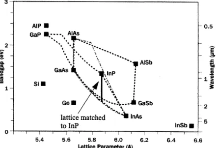
Figure 2.1 Diagram of semiconductor material bandgap versus lattice constant. The black line indicates
InGaAsP compositions lattice-matched to InP. . . . ... 22
Figure 2.2 (a) 3-D, or bulk, electron diffraction from a rough InP surface. (b) Electron diffraction from an ordered,yetrough, surface. (c) 2-D,orsurface, electrondiffractionfromasmoothInP surface along [0 11].
. . . .. . . .. . . . .. . . ... .. .. . ... . . .. . . . . .. . . . .. . . . .. . . .. . . . .. . . . 2 7
Figure 2.3 4-fold RHEED pattern from an InP surface along [011] . ... 28
Figure 2.4 Diagram of the integrated II-VI/III-V system. All samples are introduced into the system via
the Introduction Chamber ... 29
Figure 2.5 Diagram of the photoluminescence setup used for measurements presented in this thesis. The
highpass filter passes wavelengths greater than 550 nm . ... 33
Figure 2.6 (a) Nomarski microscopy image (200x magnification) of -2 pm InP (lightly Si-doped)
deposited on an InP substrate. Growth conditions: rate - 0.7 pm/br, Tsub - 480'C, chamber pressure
- 3x10⁻⁵ Torr, and V/III - 10. (b) Nomarski microscopy image (200x magnification) of -0.17 pm InP and
-0.07 pm InGaAs deposited on an InP substrate. Growth conditions for InP: rate -0.35 pnm/hr, Tsub
-470'C, chamber pressure -1.9x10⁻⁵ Torr, V/III - 13. The ramped nucleation procedure was utilized in (b)
only ... 35
Figure 2.7 Nomarski microscopy image (200x magnification) of -0.25 pm of InP (and 2 InGaAs quantum wells) deposited on a GaAs substrate. Growth conditions for InP: rate -0.35 pm/hr, Tsub -470'C, chamber
pressure -1.9x10⁻⁵ Torr, V/III - 13. Note: the surface is slightly rough, but not unexpected due to the large
lattice-m ism atch . ... 37
Figure 2.8 Nomarski microscopy image (200x magnification) a typical AlGaAs/GaAs surface grown by
GSMBE. 500 nm of Al(J.X)GaxAs (x - 0.85) deposited on GaAs. ... 38
Figure 2.9 Calculation of the miscibility gap for InGaAsP materials, using the regular solution approximation for the solid solution (after [40]). The area within each ring designates the miscibility gap for a given substrate temperature. The diagonal line represents the compositions of InGaAsP lattice-matched to InP [following Eq. (2.4)]. The filled-in circles are compositions that have been deposited in the GSMBE
system at MIT. 4700C is the approximate substrate temperature used for layers and structures presented in
this thesis . ... 41
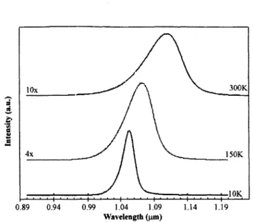
Figure 2.10 PL at various temperatures for -280 nm of In(JX)GaxAsyP(Jy) (x - 0.12, y - 0.3), slightly
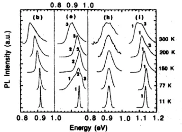
Figure 2.11 PL measurements at multiple temperatures illuminating the spectral dependence of
compositional modulation. Sample (b) is a compressive-strained InGaAsP (x-0.25, y-0.7) layer just inside
the calculated miscibility gap. Sample (e) is a lattice-matched InGaAsP (x-0.33, y-0.7) layer within the
calculated miscibility gap. Sample (h) is a tensile-strained InGaAsP (x-0.4, y-0.7) layer within the
miscibility gap. Sample (i) is a tensile-strained InGaAsP (x-0.25, y-0.37) layer just inside the calculated
miscibility gap. Figure from [13] . ... 43
Figure 2.12 PL at various temperatures for - 470 nm of Inj.-,GaxAs (x - 0.494), slightly tensile-strained.
Graphs are offset for clarity. Peaks labeled "G" correspond to GaAs-rich features, peaks labeled "N" correspond to the expected InGaAs features, and peaks labeled "I" correpond to InAs-rich features.... 43
Figure 2.13 PL at various temperatures for -200 nm of Inj..xGaxAs (x - 0.47), deposited on InP. Graphs
are offset for clarity. Peak labeled "N" is attributed to the average InGaAs composition ... 45
Figure 3.1 (a) -245 nm of InP, containing two InGaAs quantum wells centered -220 nm from the GaAs,
deposited on a GaAs/AlAs DBR. (b) -245 nm of InP, containing four quantum wells centered within the
InP layer, deposited on a GaAs/AlAs DBR . ... 49
Figure 3.2 Nomarski contrast microscopy image of - 250 nm of InP (containing two InGaAs quantum
wells) deposited on a GaAs-terminated DBR. Magnification is 200x... 50
Figure 3.3 300K PL spectrum of -250 nm of InP containing two InGaAs quantum wells (centered
- 220 nm from the GaAs-InP interface) deposited on GaAs . ... 51
Figure 3.4 HRDAXD scan of a -250 nm InP/InGaAs region deposited on a GaAs/AlAs DBR . ... 51
Figure 3.5 Auger Electron Spectroscopy scans of a patterned InP surface and the surface of an InP epi-ready wafer. The relative magnitude of elements on the surface of both samples is nearly identical. 54
Figure 3.6 (a) Scanning electron micrograph of an InP rectangular-patterned grating. (b) (400) reciprocal
space map of the grating shown in (a) . ... 54
Figure 3.7 {422} reciprocal space map of the corrugated InP surface shown in Figure 3.6(b) . ... 55
Figure 3.8 TAD (400) Ao scan for InGaAsP grown on a rectangular-patterned InP grating. The grey line
is data obtained from a sample exposed to a P2 flux prior to nucleation, whereas the black line is data
obtained from a sample exposed to an As2/P2 flux mixture... 56
Figure 3.9 (a) SEM of a thermally cleaned InP grating. (b) SEM of a low temperature atomic
hydrogen-cleaned InP grating. On both samples, the overlayer is InGaAs nominally lattice matched to InP ... 57
Figure 3.10 Sputtering Auger electron spectroscopy scan of an InGaAs/patterned-InP-surface interface.
The absence of both C and 0 suggests a very clean patterned InP surface prior to overgrowth. ... 58
Figure 3.11 Auger electron spectroscopy scan of the surface of an InP grating prior to any pre-epitaxy
cleaning. Surface concentrations of C and 0 are -58% and -12%, respectively... 58
Figure 4.1 Calculated power in the dropped channel for a Bragg-resonant channel-dropping filter. (a)
Calculated power for resonators with rectangular index modulations and (b) for resonators with sinusoidal
index modulations. Calculation by J.N. Damask, MIT . ... 61
Figure 4.2 (a) Diagram of a sawtooth-patterned corrugation with (h l1)A sidewalls. (b) Diagram of (a)
following mass-transport alteration of the grating profile . ... 61
Figure 4.3 Cross-sectional transmission electron microscopy image of (a) InGaAsP deposited via OMVPE
on a preserved sawtooth-patterned InP grating, and (b) a DFB laser structure deposited via OMVPE on a
Figure 4.4 Schematic illustration of the proposed overgrowth of InGaAs(P) on submicron period sawtooth-patterned (100) InP substrates containing (hl 1)A sidewalls. The starting grating pattern in InP is
outlined in black . ... 63
Figure 4.5 Schematic diagram of a generic overgrown structure on a rectangular-patterned surface. (w: tooth width at the tooth midpoint, d: tooth depth, F: grating width, A: grating period, t: overgrown layer
thickness) . ... 67
Figure 4.6 10K PL spectra of InP deposited on: untreated InGaAsP epilayer (black line), 30 sec. wet chemically etched InGaAsP epilayer (dark gray line), InGaAsP epilayer with -100 nm removed via RIE (gray line), and -100 nm-deep InGaAsP gratings (light gray line). Data is offset for clarity. ... 68 Figure 4.7 (a) SEM image of gratings fabricated in an InGaAsP epilayer. (b) (400) RSM of the gratings depicted in (a). (c) {422} glancing exit RSM of -1 pm of InP deposited on the InGaAsP gratings depicted in (a). Intensity scale for (b) and (c) is 1-1x10⁴ ... . . . 69
Figure 4.8 AFM images of -1 pm of InP deposited on the InGaAsP gratings shown in Figure 4.7(a). The white line in the image to the right is the profile of the gratings traced from Figure 4.7(a) . ... 70
Figure 4.9 (a) (400) RSM of -2 10 nm of InGaAsP deposited on a planar InP substrate. (b) (400) RSM of
-210 nm of InGaAsP deposited on rectangular-patterned InP gratings. Intensity scale is 1- 1x10⁴. .... 73
Figure 4.10 Aqx = 0 scans (6/26 scans) of the planar sample (from Figure 4.9(a), gray line) and of the grating overgrowth sample (from Figure 4.9(b), black line). Data is offset for clarity . ... 74
Figure 4.11 {422} RSM of -210 nm of InGaAsP deposited on rectangular-patterned InP gratings. The
white lines indicate diffraction envelope shifts. The intensity scale is 1 -lx . .... 75
Figure 4.12 Glancing incidence {422} RSM of -210 nm of InGaAsP deposited on an InP rectangular-patterned grating. The x-rays are incident parallel to the surface corrugation. The analyzer and monochrometer streaks are a function of the TAD measurement setup [57]. Both streaks are apparent due
to the dispersive arrangement of the TAD system during this measurement... 76
Figure 4.13 (a) HRDAXD of -200 nm of InGaAs deposited on a preserved rectangular-patterned InP grating (black curve). The gray curve is data obtained from the simultaneously grown planar monitor sample. A SEM of the sample is depicted in Figure 3.9(b). (b) HRDAXD data from -200 nm of InGaAs deposited on a slightly altered rectangular-patterned InP surface. A SEM of the sample is depicted in Figure 3.9(a). The gray curve is data obtained from the simultaneously grown planar monitor sample . ... 78 Figure 4.14 10K PL spectrum of -200 nm InGaAs deposited on a preserved InP rectangular-patterned
grating. See Figure 3.6(b) for a cross-sectional SEM of the sample. ... 79
Figure 4.15 Schematic illustration of the overgrowth process of InGaAs(P) on rectangular-patterned (100)
InP surfaces ... 79
Figure 4.16 300K PL spectra of -210 nm of InGaAsP deposited on a preserved InP grating (black line)
and the simultaneously grown monitor sample (gray line) . ... 82
Figure 4.17 (a) X-ray topography measurement of -210 nm of InGaAsP deposited on an InP rectangular-patterned grating. The absence of distinct features suggests material of good quality having a low defect density. (b) X-ray topography measurement of InGaAs deposited on an InP substrate. The distinctive lines
indicate the presence of misfit dislocations . ... 83
Figure 4.18 Scanning transmission electron microscopy measurement of the sample analyzed in Figure
4.9(a); -210 nm of InGaAsP deposited on an InP substrate ... 84
Figure 4.19 TAD-generated {311} glancing exit RSM of In(J.X)GaAs (.y) (x - 0.12, y - 0.3) overlayer
Figure 4.20 TAD-generated (400) RSM of Ing0_x)Ga AsYP jy) (x~0.12, y-0.3) overlayer on a
rectangular-patterned InP grating. RSM intensity scale is 1-1x10 ... 85
Figure 4.21 An extreme example of roughness in the grating trenches of -230 nm period InP gratings
fabricated via RIE ... ... 86
Figure 4.22 -230 nm period gratings fabricated in an InGaAsP epilayer; gratings have been wet chemically etched for entry into the GSMBE system. The roughness apparent in the grating trenches detrimentally
affects the quality of an InP overlayer . ... 86
Figure 4.23 (400) RSM of -275 nm InP deposited on the InGaAsP grating shown in Figure 4.22. Intensity scale is 1-1x 10 4... . . . 87 Figure 4.24 SEM image of the -230 nm period InP gratings discussed in Section 4.2.2. The gratings have
been degreased and wet chemically etched following RIE. Note the smoothness of the grating trenches. 88
Figure 4.25 Scanning electron micrograph of InGaAsP gratings with a thin layer of the Ti etch mask
remaining on the grating teeth . ... 88
Figure 4.26 Normarski interference contrast microscopy image of -3.5 ptm of InP deposited on InGaAsP
having a thin layer of the Ti etch mask on the InGaAsP surface (200x magnification). The rough edge
apparent in the photo is the edge of the Ti mask . ... 89
Figure 4.27 Schematic of deposition in rectangular trenches and on mesas as determined via the numerical model developed by Biasol and Kapon. Figure from [89]. The sl superscripts represent the self-limiting
widths; Ar = r, - rb - - - ---... 90
Figure 4.28 Calculation of the variation in the Ga diffusion length for different surface orientations. Figure
from [110]. ... 92
Figure 4.29 Schematic of GaAs deposition on a 0.5 ptm GaAs rectangular mesa as determined via the
numerical model developed by Ohtsuka. Figure from [110] . ... 92
Figure 5.1 Measured transmission spectrum of a 22-pair GaAs/AlAs DBR... 99
Figure 5.2 Saturable absorber design in which the absorbing quantum wells are located near the null of the
electric field (at ? - 1.54 pm) within the structure. The electric field is calculated as a function of position
from the GaAs substrate; in order to obtain the intensity within the structure the electric field should be multiplied by the refractive index. A dielectric antireflection coating is also present on this structure. 100
Figure 5.3 Saturable absorber design in which the absorbing quantum wells are located near the maximum
of the electric field (at X - 1.54 pm) within the structure. The electric field is calculated as a function of
position from the GaAs substrate; in order to obtain the intensity within the structure the electric field should be multiplied by the refractive index. A 5-layer dielectric resonant coating is also present on this structure.
. . . .. . . . .. . . . 10 1
Figure 5.4 Saturation fluence measurement of the structure shown in Figure 5.2. The inset depicts the pump-probe measurement at -80 pJ/cm2 .... . . .
102 Figure 5.5 Saturation fluence measurements of the structure depicted in Figure 5.3. Inset (i) is a
pump-probe measurement at -10 pJ/cm2; inset (ii) is a pump probe measurement at -200 pJ/cm2 . . .
102 Figure 5.6 Calculated stability contours for a fast saturable absorber locked laser. Q-switched
mode-locking is present in regions labeled "Unstable". The area within the dotted line is the unstable region with
TPA included in the model... 104
Figure 5.7 Diagram of the mode-locked fiber laser containing an Er/Yb codoped phosphate glass
Figure 5.8 Schematic of an actively harmonically mode-locked fiber laser stabilized with a TPA structure.
.. . . ... . . .. . . . .. . . . .. .. .. . .. .. .... . .. .. . ... .. . .. . . .. . . . .. . . . .. . . . .. . . 10 6
Figure 5.9 Simulation of the reflectivity spectrum of a 6-pair GaAs/Al.Oy DBR. The dark trace assumes
10% contraction of the AlxOY layer resulting from the oxidation process... 108
Figure 5.10 Nomarski interference contrast image (200x magnification) of the surface of the structure depicted in Figure 5.2. The slip lines and wire-like pieces are the result of oxidation of the AlAs layers in the DBR . ... 109
Figure 6.1 Depiction of the three regimes of operation for a SOA... 113
Figure 6.2 (a) Calculated phase response of a SOA a a continuous train of intense pulses. (b) Calculated phase response of a SOA to a variable train of intense pulses. Figures from [165] ... 114
Figure 6.3 Diagram of the ultrafast nonlinear interferometer (UNI). PSI is polarization-sensitive isolator, SOA is semiconductor optical amplifier, BRF is birefringent fiber, and PC is polarization controller. . 115 Figure 6.4 Diagram of strain effects on energy band arrangements in semiconductor materials. Diagram after [109]. ... 117
Figure 6.5 Schematic of the current SOA structure under development... 120
Figure 6.6 (a) 3-D mode solver solution for a TE mode supported in a 2.5 pm ridge SOA structure (structure depicted in Figure 6.5). Depicted is the electric field intensity. (b) Horizontal and (c) vertical cross-section of the TE mode intensity graphed along with the index profile of the structure. ... 121
Figure 6.7 (a) 3-D mode solver solution for a TM mode supported in a 2.5 pm ridge SOA structure (structure depicted in Figure 6.5). Depicted is the electric field intensity. (b) Horizontal and (c) vertical cross-section of the TM mode intensity graphed along with the index profile of the structure... 122
Figure 6.8 Diagrams of the simulated electric field amplitude for the TE mode and TM mode in the SOA structure of Figure 6.5 ... 123
Figure 6.9 Schematics of other double heterostructure SOA designs being considered ... 123
Figure A.1 Geometric representation of Bragg's Law. The path length difference between two layers is A B C . ... 132
Figure A.2 Geometrical representation of the Ewald sphere construction . ... 133
Figure A.3 The Ewald sphere constructed in reciprocal space. The (400) diffraction conditions are not satisfied in (a). The (400) diffraction conditions are satisfied in (b). Figure from [177] ... 134
Figure A.4 Diagram of available diffraction conditions for (100) Si. 134 Figure A.5 Geometrical depiction of diffraction of an incident source having a linewidth
P1/2
due to an angular deviation, c, from the Bragg condition. Figure from [31] ... 135Figure A.6 Basic diffraction geometries for symmetric and asymmetric arrangements ... 136
Figure A.7 Diagram of diffraction geometries . ... 137
Figure A.8 General high-resolution double axis x-ray diffraction arrangement ... 138
Figure A.9 Rocking curves depicting the increased beam conditioning obtained with an increase in the number of diffractions from a (220)-oriented Si crystal. Figure from [177] . ... 139 Figure A.10 Arrangement for a (400) 0/20 scan in reciprocal space. An example of a double axis 0/20
measurement of an InGaAsP (x - 0.4 2, y - 0.81) epilayer deposited on an InP substrate is shown to the right.
Figure A.11 An asymmetric {422} 0/20 scan depicted in reciprocal lattice space... 142
Figure A.12 Generic diagram of a triple axis x-ray diffractometry system. The conditioning crystals are typically configured in either a 2- or 4-bounce arrangement. Likewise, the analyzer crystal is typically configured in either a 2- or 4-bounce arrangement (or possibly a 3-bounce arrangement, depending on the
crystal m aterial) . ... 143
Figure A.13 Diagram of the Bede D3 diffractometer used at UCLA . ... 143
Figure A.14 Generic reciprocal space diagrams of reciprocal space map generation... 145
Figure A.15 Depiction of relaxation and curvature directions in asymmetric RSMs. Note, the figure on the
left is a glancing incidence arrangement and the figure on the right is glancing exit. ... 146
Figure A.16 (a) (400) RSM of a rectangular-patterned InP substrate measured on a Philips MRD at Lincoln
Laboratory. (b) (400) RSM of the same patterned substrate measured on the Bede D3 at MIT . ...
147
1
Introduction
1.1 Motivation
The need for ultrafast (greater than 100 Gbps) all-optical communication networks is amplified as the amount of data-containing communication traffic continues to grow at an exorbitant rate. Within North America, market research indicates that the volume of data traffic has surpassed that of voice traffic on the telecommunications network [1]. Shown in Figure 1.1 is the current and forecasted Internet-related data traffic. Current terrestrial communication networks combine the well-developed electronic components
Figure 1.1 Graph of current and forecasted Internet-related traffic on the
communications network in North America. Figure from [1].
(i.e. switching and routing) with the more recent optical propagation schemes. The method chosen to address the need to increase the aggregate data rate of the networks, in order to meet the demands driven in large part by the Internet, is to multiplex the data. Two standard (de)multiplexing schemes are geared towards terrestrial communication networks: wavelength division multiplexing (WDM) and time division
multiplexing (TDM). Multiplexing schemes are attractive, as they enable increased transmission over
silica fiber already buried and in use.
Although WDM systems are in the process of being implemented, aggregate data rates may be limited
by electronic signal processing speeds at the originating and terminating ends of the fiber transmission
lines. The upper limit for operating speeds of electronic components is not yet established, however it is
currently lower than achievable optical transmission speeds. The ability to move away from electronic
processing and towards all-optical processing of the network-level data is attractive due to the simplicity of
integration and the possible elimination of optoelectronic conversion.
In order to eliminate electronic processing on the network level, all-optical processing components
must transfer, store, and rate-convert all data to and from the data rate of the source (i.e. a computer or a
router) to the network data transmission rate. Thus, components such as passive wavelength-selective
routers and all-optical switching mechanisms need to be implemented. Additionally, ultrafast
(femtosecond) optical sources providing high bit data and clock rates are required for network transmission
rates greater than 1 Thps.
The multiplexing of a data segment, or word, onto multiple wavelengths allows an N times increase in
the network transmission rate, where N is the number of wavelengths. Current systems (i.e. the WaveStar
400G manufactured by Lucent Technologies [2]) support 80 wavelengths in which the data carried by each
wavelength has a base data rate of 2.5 Gbps (OC-48), making the effective transmission rate 200 Gbps.
The WaveStar can also support OC-192 transmission rates (10 Gbps), and will multiplex 40 channels for
an aggregate data rate of 400 Gbps. Although the severity is not yet clear, a future limitation of WDM is
the minimum achievable spacing between the wavelength channels. In order to more closely space the
channels, issues such as the linewidth of the optical source and the ability to maintain signal-to-noise ratios
must be addressed. Furthermore, the selectivity of all-optical devices within the network must match that
of the channel spacing. Thus, both material quality and fabrication techniques of the network components
affect the ultimate network performance.
One of the key components enabling WDM propagation is the distributed feedback (DFB) laser. A
periodic index modulation, typically buried within the device structure (hence requiring an overgrowth
step), is used to select the specific operating wavelength of the laser. Although DFB lasers have been
commercially available for more than 10 years, fabrication of these devices is still problematic.
Furthermore, as the WDM wavelength spacing continues to decrease, the increasing demands placed on
the fabrication of the DFB lasers bring the fabrication issues to the forefront. Similar patterned surface
overgrowth issues need to be addressed for realization of wavelength-selective filters, e.g. Bragg-resonant
filters, for all-optical routing. For closely spaced wavelength channels, the selectivity of the filters must
likewise increase. Thus, issues pertaining to the corrugation definition (via lithography) as well as to the
overgrowth (in regards to profile alteration) must be addressed for realization of future WDM network
components.
Time division multiplexing of data streams has similar bandwidth requirements as does the WDM
scheme. TDM propagation schemes, like WDM, can consist of multiple data streams propagating at lower
data rates. The multiplexing in this instance is performed in the time domain, i.e. bit interleaving or slot allocation. Various TDM-based network geometries have been developed in recent years, such as the helical local area network (HLAN) [3] and an all-optical packet routing architecture [4]. Of importance to TDM-based propagation schemes is the multiplexing and demultiplexing of the ultrafast data streams. In existing systems, for propagation rates on the order of Tbps, the data must be optically demultiplexed to data rates that the electronic components can process. Optoelectronic conversion must be performed not only at the edges of the network (i.e. for interfacing with a computer) but also along the network for switching and routing functions. All-optical switching as well as optical (de)multiplexing are very attractive alternatives to optoelectronic conversion. Optical switching and demultiplexing of TDM data has recently been demonstrated via various interferometric techniques (i.e. ultrafast nonlinear interferometers, semiconductor laser amplifiers in a loop mirror, etc.). Many optical switching schemes require the use of a semiconductor optical amplifier (SOA) as the nonlinear medium, as well as optical clock sources with repetition rates on the order of GHz (for integration with electronic components).
For TDM network propagation rates on the order of Tbps, lasers must be capable of producing pulses shorter than a picosecond. One method of ultrashort pulse generation in laser cavities is mode-locking. Mode-locking forces the temporal modes in a cavity to propagate in phase, and can be instigated either actively or passively. Passive mode-locking is typically preferred primarily due to ease of implementation and lack of external control. A semiconductor saturable absorber mirror is a monolithically integrated device utilized for passive mode-locking of a wide variety of lasers. The monolithic integration of an absorber with a mirror enables the replacement of a high reflector in a laser cavity with the absorber mirror, effectively leaving the number of components in the laser cavity unchanged.
Entrenched in the requirements for the realization of all-optical communication networks is the need for a highly nonlinear medium suitable for ultrafast switching. In order to implement all-optical networking schemes, the current switching, storage, clock recovery, etc. accomplished by electronic components must be performed in the optical domain. In recent years, various all-optical switching techniques utilizing semiconductor optical amplifiers (SOAs) have been demonstrated at reported data rates up to 1.5 Tbps [i.e. 5,6,7,8]. More recently, monolithic integration of all-optical switching schemes has been accomplished in InP-based materials [i.e. 9]. Requirements placed on the SOAs include the need for polarization insensitivity and as well as large intensity induced nonlinearities in the shortest possible device lengths.
1.2 Thesis Overview
This thesis addresses many aspects of the development of semiconductor components for all-optical communication networks. The ability to master the use of gas source molecular beam epitaxy (GSMBE) to realize devices based in InP and GaAs materials systems is a large part of this thesis, and will be discussed in detail in Chapter 2. The use of a low temperature atomic hydrogen-assisted oxide removal technique for both regrowth on GaAs/AlAs structures as well as overgrowth of surface corrugations in In(Ga,As)P
materials is addressed in Chapter 3. The realization of buried index contrasts, in which the modulation is unaltered from the fabricated profile, has been accomplished via the use of a low temperature atomic hydrogen-assisted oxide removal process and GSMBE. Preservation of the fabricated profile affords increased flexibility in device design as well as an anticipated decrease in compositional modulation in the deposited overlayer. Analysis of the resulting structures containing buried-index contrasts is addressed in Chapter 4. The design of semiconductor saturable absorber mirrors for implementation in fiber-based laser
cavities is presented in Chapter 5. Preliminary development of SOAs for implementation in an ultrafast
nonlinear interferometer has also been investigated; associated preliminary designs and simulations are presented in Chapter 6. Finally, Chapter 7 encompasses a summary as well as suggestions for extensions of
2
Gas Source Molecular Beam Epitaxy of
(In,Ga)(As,P) Materials
The use of Gas Source Molecular Beam Epitaxy (GSMBE) for the realization of high speed communication components, both optical and optoelectronic, is the backbone of this thesis. Specifically, the ability to utilize GSMBE for deposition of (In,Ga)(As,P) materials on both InP and GaAs substrates, either planar or patterned, is addressed. Both the growth technique and the subsequent analysis (both
in-situ and ex-situ) of the resulting material and/or structures will be discussed. Thus far, specific issues
being addressed in regard to materials growth include the effect of the oxide desorption technique and V/ III ratio on the generation of defects.
2.1 (In,Ga)(As,P) Materials
The ability to deposit high quality InP-based materials for the fabrication of optical devices is an important aspect of the development of all-optical communication network components. The central
material of interest is In ixGaxAsyPI-y; these quaternary materials are quite attractive due to the wide range
of achievable bandgaps with lattice constants matching that of an InP substrate (0.75eV of InGaAs to 1.35eV of InP). Depicted in Figure 2.1 is the bandgap versus lattice parameter space for a wide range of materials. The solid line indicates the range of InGaAsP materials with the same lattice constant as InP. With the current state of the communications market, the demand for InP-based emitters and detectors exceeds that able to be supplied [10]. Additionally, performance specifications for both optical and electrical devices are placing ever more stringent requirements on the materials growth and fabrication processes used to realize the devices [11]. Unlike GaAs, which has been investigated in detail for material
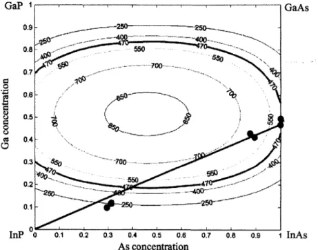
properties as well as device implementation, deposition of InGaAsP is still plagued with issues as basic as substrate quality (many manufacturing lines still use 2"-diameter InP wafers whereas GaAs manufacturing lines are moving to 6"-diameter wafers). Furthermore, deposition of InGaAsP is inherently more difficult strictly due to the need to precisely control the deposition rate and relative ratio of four elements, two of which are group V elements; in comparison, materials typically deposited on GaAs contain only a single group V element. InGaAsP is also susceptible to spinodal-like decomposition; given the correct (or incorrect) growth parameters, an epilayer can experience lateral compositional modulation with the result being GaP- and InAs-rich regions throughout the layer [12,13]. Although growth parameter dependent, InGaAsP having X-1.1-1.3 pgm is often quoted as being the most difficult quaternary to deposit [14].
However, reports have also been published in regards to difficulty in depositing InGaAsP with X near 1.55
im, especially if the quaternary is tensile-strained [13]. Even though much is known about the deposition of InGaAsP materials, much is yet to be determined in order to fabricate new devices to meet the demands of the communication-based industry.
3. AIP E 0.5 GaP E - - AlAs 2--"" C** AISb GaAs C Sim Ge - GaSb 2
lattice matched InAs 5
to InP InSb N
0
5.4 5.6 5.8 6.0 6.2 6.4 6.6
Lattice Parameter (A)
Figure 2.1 Diagram of semiconductor material bandgap versus lattice
constant. The black line indicates InGaAsP compositions lattice-matched to
InP.
2.1.1 Molar Composition Determination
As can be seen from Figure 2.1, the range of bandgaps for which InGaAsP is lattice-matched to InP is determined by the relative concentration of the four elements. In addition to being concerned about the bandgap, the lattice constant must also be taken into consideration. The ratio of both the group III elements and the group V elements must be set in order to obtain the desired bandgap and lattice constant.
For the derivation of various material properties of ternaries and quaternaries, a linear interpolation, dependent on the binary compounds that compose the material, is generally a reasonable approximation when experimentally determined expressions are not available. The equations for ternary and quaternary compounds of AxB._xC and AxB _xCyDy are:
P(AXBI
_XC) = xPAc +(1 -x)PBcEq.
(2.1)P(AXB1 _CDI _) = XYPA C + x(1 -Y)PAD +
y(
-x)PBc +(
-x)( -Y)BD Eq. (2.2)where P is any material property that can be interpolated. These equations may be used in general for calculating material properties such as lattice constant, refractive index, elastic stiffness constants, etc. The linear variation in lattice constant with respect to composition is known as Vegard's Law [15], and for In j,GaxAsyP., is
a(x,y) = 0.1896y-0.4175x+0.0124xy+ 5.8687 Eq. (2.3)
Rewriting Eq. (2.3) for InGaAsP lattice-matched to InP, the mole fractions, x and y, can be approximated by
x ~ 0.47y Eq. (2.4)
The bandgap equations for ternaries and quaternaries are derived from semiconductor band theory and experimental measurement techniques, such as photoluminescence, ellipsometry, etc. The experimentally obtained InGaAsP direct energy gap equation [11] is
Eg(x, y) = 1.35 + 0.668x - 1.068y + 0.758x2 + 0.078y2 - 0.069xy - 0.322x2y + 0.03xy2 Eq. (2.5)
2.2 Gas Source Molecular Beam Epitaxy
Molecular Beam Epitaxy (MBE) is a semiconductor material deposition technique developed in the late 1960s that is performed in an UtraHigh Vacuum (UHV) environment. The source material is supplied in a pure, solid elemental form and a heated semiconductor substrate acts as the template for deposition of crystalline material. The deposited semiconductor material crystallizes as the incident atoms migrate along the surface of the sample, and find a lowest energy location (i.e. preferred incorporation site) at which the atomic bonds are satisfied. The elemental source material is located in heated ovens that generate atomic or molecular beams of material via vaporization; the beams are controlled (blocked or not blocked from the
path to the substrate) via metallic shutters. In an UHV environment (i.e. 10~8 to 10-10 Torr) the generated atomic or molecular beams have a line-of-sight path to the semiconductor substrate. The molar composition of the elements within the deposited crystal is a function of the ratio of the elements incident on the semiconductor substrate. Doping of the semiconductor is a function of the relative arrival rate of the elements and dopant atoms at the sample surface. Typical growth rates for semiconductor materials via MBE are -1 ptm/hr.
The use of Gas Source Molecular Beam Epitaxy (GSMBE) for semiconductor materials growth has been in existence since the late 1970s [16]. The technique, based on MBE, is a marriage of solid sources and gaseous sources. By the mid- to late 1970s, MBE produced the most abrupt interfaces, the most accurate compositional changes, and the most controlled doping profiles. Initial attempts to deposit InGaAsP on InP via MBE were relatively unsuccessful due to the lack of a high quality source for
generation of a stable P2 flux. The early methods of using solid phosphorus involved vaporizing red
phosphorus, P4, directly. This method has multiple inherent difficulties, including: (1) P4 is composed of
various allotropic forms in which each form has a different vapor pressure, (2) P4 has an extremely short
lifetime on the sample surface and without an excessive flux during growth, In-rich material will be
deposited, and (3) due to the excessive amounts of P4 needed, a build-up of elemental (white) phosphorus,
P, occurs in the growth chamber deteriorating the UHV environment necessary for MBE growth. The other common growth methods at the time, i.e. Liquid Phase Epitaxy (LPE) and Metal Organic Chemical Vapor Deposition (MOCVD), were likewise plagued by a set of inherent problems, such as interface grading and lack of control over the doping profile [16]. Thus, the need for a growth method that would combine the qualities of MBE and a constant phosphorus flux (without a by-product of white phosphorus) prompted the development of GSMBE [16].
GSMBE is essentially conventional MBE with group V elements supplied in the form of hydrides.
Under typical MBE growth conditions, the rate of material deposition is essentially controlled via the supply rate of the group III element(s), whether the group V elements are supplied in solid or gaseous form. Thus, GSMBE takes advantage of the precise control of layer thickness (and associated deposition rate) achievable with the MBE technique. Although the low pressure and atmospheric pressure growth methods, such as MOCVD, tend to be preferred in manufacturing settings (e.g. due to less down time for routine maintenance, and less material build-up on the walls of the reactor) the UHV environment of MBE produces purer material with well-defined surfaces and interfaces [17]. Additionally, within the MBE growth environment, deposition of individual monolayers can be achieved (e.g. Migration-Enhanced Epitaxy (MEE) [18] or Atomic Layer Epitaxy (ALE) [31]).
The atomic beams of group III elements (i.e. In, Ga, Al) are generated in both MBE and GSMBE by heating of an effusion cell. An effusion cell is an oven comprised of a ceramic Pyrolytic Boron Nitride (PBN) crucible surrounded by a heating coil, in which the solid elemental material is placed within the
crucible. The effusion cells are heated to temperatures ranging between 750'C and 12000C (material
dependant), at which point a molecular beam (or flux of material) is generated via vaporization [16]. The vaporized material in the effusion cells is blocked from the semiconductor substrate surface by a molybdenum or tantalum shutter. For growth, the shutter is opened for an interval of time corresponding to the desired thickness of the material being deposited, with a simultaneous provision of a group V flux.
A disadvantage of the effusion cell is the nonuniform flux generated as a result of the system geometry
and the cosinusoidal distribution of molecules leaving the cell. However, this nonuniformity is rather adequately negated by rotating the semiconductor substrate, resulting in a more uniform distribution of atoms across the entire semiconductor surface. Additionally, the development of crucibles with narrower openings (i.e. the Sumo Cell manufactured by EPI [19]) and conical-shaped crucibles further enhance the flux uniformity.
The group V elements in GSMBE are generated from the hydrides phosphine, PH3, and arsine, AsH3
-An advantage of using gaseous group V elements is the near instantaneous flux changes achievable as
compared to the solid source alternative. The decomposition of the hydrides from MH3 to M2 and H2 is
accomplished by passing the pure (99.999%) hydride through a high-temperature-low-pressure gas cell. This gas cell is also known as a "cracker" since it thermally decomposes (or cracks) the hydrides at
temperatures between 9000C and 11000C. The internal arrangement of the cracking cell is such that the
hydride is passed through a pyrolytic boron nitride (PBN) tube followed by a high temperature zone containing high purity PBN chips. The thermal cracking takes place in the high temperature zone when the hydride is in contact with the PBN chips [20]. The use of a mass flow controller (MFC) further enhances the attractiveness of gaseous group V sources as the MFCs accurately control the rate at which the hydrides
enter the cracker. Since the cracking efficiency of AsH3 and PH3 is nearly 100% for cracker temperatures
between 900-11000C [20], the flux impinging on the semiconductor surface is likewise well controlled. In
addition to precise flux control, MFCs offer more accurate and timely changes in hydride flow rates. The MBE environment is typically cleaner than other growth environments, in many regards due to the
ultralow pressure environment. In either atmospheric or low pressure (- 76 Torr) MOCVD, the gases are
introduced into the susceptor as hydrides and organometallics, and the cracking of the hydrogen and carbon molecules is performed in a 'boundary layer' [21]. The boundary layer is located at the surface of the semiconductor sample. If the temperature of the sample is such that the carbon and hydrogen molecules are separated from the group III atoms, the elements will then be able to incorporate into the
semiconductor crystal structure. Although GSMBE also utilizes hydrides for the group V sources, the hydrogen is separated from the group V atoms upon entry into the UHV environment, generating H2 and
group V dimers. The H2 by-product is not harmful to semiconductor growth, and most likely does not
affect the growing crystal because of the excessive temperatures required to break a H-H bond. For
example, the cracking efficiency for H2 passed through a PBN tube containing a tungsten filament held at
-21 000C is only -3% [22]. Although the H2 generated via cracking of the hydrides does not directly affect
the growing crystal, the overpressure due to the H2 in the GSMBE reactor may limit the maximum
achievable group V flux (pumping system dependent).
An additional advantage of GSMBE being an extension of conventional MBE is that the well developed in-situ surface analysis technique, Reflection High Energy Electron Diffraction (RHEED), may be utilized. The electrons diffracted from the surface of the semiconductor substrate are directed to a
phosphorus-coated screen for observation. These electrons typically have energies between 5 and 50 KeV.
(GS)MBE is particularly suited for RHEED not only because of the effective line-of-sight in a UHV
environment, but also because the internal arrangement of MBE-type machines are such that the electrons are incident on the semiconductor sample at a slight angle (1-3 degrees), and do not interfere with the placement of the molecular sources. A small incidence angle is desired in order to limit the depth in which the electron penetrates the semiconductor material. By limiting the penetration depth, the electron beam is sensitive to changes on the surface of the semiconductor. Thus, the surface can be monitored during deposition, and the status of the growth can be determined by monitoring the resulting RHEED pattern. In order to diffract from the semiconductor surface, the wavelength of the electron must be on the order of, or
smaller than, the lattice constant; for high energy electrons (5-50 KeV) the deBroglie wavelength range is
0.17-0.06
A.
A RHEED pattern is generated by the interference of the diffracted electrons. Analogous to multiple
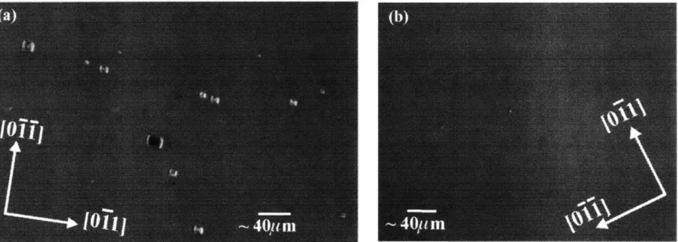
slit optical diffraction, diffraction from a crystal lattice produces the Fourier Transform of the periodic lattice. Thus, each lattice arrangement will have a characteristic RHEED pattern. Since RHEED is sensitive to the surface of the semiconductor, the diffracted pattern will be altered if there is any type of surface structure, e.g. steps or islands. Typically, a rough surface, or a randomly oriented three-dimensional surface, results in a spotty "bulk" RHEED pattern, as shown in Figure 2.2(a), since the diffracted electrons penetrate the sample and diffract from the 3-D features on the surface. A bulk RHEED pattern is typical of a semiconductor substrate prior to material deposition. An epitaxial layer of thickness that has surpassed the critical thickness (the thickness to which the deposited layer can maintain any lattice-mismatch-induced strain before relaxation begins) is also inherently rough due to strain relaxation mechanisms. However, the roughness is typically somewhat periodic. The resulting RHEED pattern from an epilayer
(a) 3-D Diffraction
(b) Ordered 3-D Diffraction
(c) 2-D Diffraction
Figure 2.2 (a) 3-D, or bulk, electron diffraction from a rough InP surface.
(b) Electron diffraction from an ordered, yet rough, surface. (c) 2-D, or
surface, electron diffraction from a smooth InP surface along [011].
that has recently surpassed the critical thickness is shown in Figure 2.2(b). A smooth surface, or a two-dimensional surface, results in a streaky surface RHEED pattern, as shown in Figure 2.2(c) since the electrons are coherently diffracted from the surface layers. Additionally, the surface RHEED pattern of a zincblende II-V (100)-oriented semiconductor surface usually differs between [011] and [011], and is dependent on the arrangement of the bonds between surface atoms, e.g. the surface reconstruction. The RHEED pattern will further differ depending on the type of atoms present on the semiconductor surface
(i.e. group III or V). Typical atomic configurations for a P-stabilized InP surface, at 4800C, are a four-fold
periodicity along [O11 and a two-fold periodicity along [011]. For an electron beam incident along [011], the resulting RHEED pattern will represent the four-fold periodicity and appear similar to see Figure 2.3. Likewise, an electron beam incident along [011] will be sensitive to the two-fold periodicity [see Figure 2.2(c)].
RHEED patterns are observed not only to monitor the quality of each layer, but also to observe surface transitions such as oxide desorption. As a native surface oxide is inherently amorphous, exposure of the crystalline substrate following oxide desorption is easily observed via RHEED. RHEED patterns are also
Figure 2.3 4-fold RHEED pattern from an InP surface along [011].
monitored in order to non-destructively determine the growth rate of deposited materials. Oscillations in time of the diffracted intensity during epitaxy correspond to the deposition of monolayers of material. The intensity is related to the changes in step edge density and the ordering of the atoms on the surface. The portions of higher intensity correspond to a smoother surface (i.e. a completed monolayer), whereas those of lower intensity represent a rough surface (i.e. partial monolayer completion). The combination of one period of high and low intensity is representative of the deposition of a single monolayer of material. RHEED oscillations are only observable within the first few minutes of layer deposition until the surface roughness reaches a steady state condition. Hence, RHEED oscillations are only apparent when there is a distinct change in the surface roughness, as in the case for growth on atomically smooth surfaces (as opposed to growth on rough 3-D surfaces).
Additional in-situ monitoring techniques that have been applied to MBE include reflectometry (for layer thickness determination), pyrometry (for sample temperature determination), and ellipsometry (for layer thickness and composition determination). Development of in-situ control of epilayer composition and thickness using an 88-wavelength ellipsometer is currently under development on the GSMBE system at MIT. Development of this technique is being performed by Dr. G.S. Petrich and S. Warnick in Prof. Leslie A. Kolodziejski's laboratory.
In the last few years, the use of GSMBE has been slowly declining. With the development of high quality solid phosphorus crackers [23,24,25], a number of GSMBE machines have been converted to solid source MBE because of safety considerations.
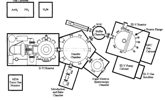
The GSMBE system used for deposition of all structures presented in this thesis is a Instruments SA Riber 32P machine. It is part of an integrated II-VI/III-V epitaxy system, as shown in Figure 2.4. All systems, both II-VI and III-V reactors, an Auger electron spectroscopy (AES) system, a sample bake-out
chamber, and an introduction chamber are connected in-situ by a transfer chamber; the base pressure of all systems is 5x10⁻⁹ Torr or lower. The solid group III sources available are Al, Ga, and two In sources. The group V materials are supplied via arsine and phosphine, and the dopant sources are solid Si and Be. The majority of the effusion cells are Riber single filament, straight-walled effusion cells with 35cc crucibles (one of the two In effusion cells is a Riber dual filament, straight-walled cell). Ceramic inserts, with an eight degree taper, have been added at the lip of each crucible in order to increase surface uniformity of the deposited material. The pumping systems on the Riber GSMBE system are a Pfieffer 2200 1/s turbomolecular pump (with an Edwards mechanical backing pump) and a CTI cryopump (as a back-up). The turbo pump is used in most cases, and always during growth, due to the higher chamber pressures
(-10-5 Torr) that result from cracking the hydrides. This system also contains an EPI hydrogen cracking
cell, for generation of atomic hydrogen for low temperature oxide removal techniques.
Gas Cabinets
AsH3 PH
11I-V Reactor
Buffer Source Flange
Chambber
C
Gas Tr .a . sferCabine
Chamber
11-VI Reactor 0Cbinet
III-V Gas
MA auger Electron Scrubber
Toxic Gas Spectroscopy
Monitor Chamber
Introduction
and Bake Chamber
Figure 2.4 Diagram of the integrated II-VI/III-V system. All samples are introduced
into the system via the Introduction Chamber.
Although the quality and rate of the GSME material deposition can be monitored in-situ via RHEED, extensive analysis of the materials and heterostructures must be accomplished ex-situ. External analysis techniques include photoluminescence (both low temperature (10K) and room temperature) for determination of material bandgap, and high resolution x-ray diffractometry for determination of the material lattice constants. In the case of InGaAsP material characterization, both photoluminescence and
x-ray diffraction measurements are analyzed in order to uniquely determine the mole fraction of all four
elements.
2.2.2 Post-Growth Material Characterization: A Brief Overview
Post-growth characterization techniques are used to determine more precisely the compositions of the
grown quaternary, and to complete a rather accurate feedback loop. The techniques utilized for layer
growth include Auger electron spectroscopy (AES), high resolution double axis x-ray diffractometry
(HRDAXD), and photoluminescence (PL). In order to accurately determine a composition, it is necessary
to use a combination of HRDAXD and a luminescence technique. As will be described in more detail in
the following sections, HRDAXD will illuminate strain in the crystal structure, whereas a luminescence
method will reveal the bandgap of the material.
Auger Electron Spectroscopy
Auger electron spectroscopy (AES) is a technique for analyzing surfaces based on the Auger process.
A surface atom, ionized via an impinging electron, may decay to a lower energy state (a doubly ionized
state) via an electronic rearrangement. The energy difference between the steady state of the atom and the
lower energy state of the doubly ionized atom is transferred to the ejected Auger electron, which will
contain a kinetic energy characteristic of the atom from which it was ejected. If this process occurs within
a few angstroms from the surface, the ejected Auger electron can be expelled without a loss of energy. This
Auger electron then generates peaks in the secondary electron energy distribution function, from which the
composition of the surface can be rather accurately identified [48].
An AES system is an UHV system consisting of an electron gun and an energy analyzer. The Auger
peaks are more accurately identified by differentiating the secondary electron energy distribution, therefore
the typical Auger spectrum is the function dN(E). The peak-to-peak amplitude of an Auger peak is related
to the atomic concentration. When not using a calibration piece (e.g. silver), the surface concentration of
some element x,
Cx,
can be approximated by
C = dI d I Eq. (2.6)