HAL Id: tel-01977195
https://tel.archives-ouvertes.fr/tel-01977195
Submitted on 10 Jan 2019HAL is a multi-disciplinary open access archive for the deposit and dissemination of sci-entific research documents, whether they are pub-lished or not. The documents may come from teaching and research institutions in France or abroad, or from public or private research centers.
L’archive ouverte pluridisciplinaire HAL, est destinée au dépôt et à la diffusion de documents scientifiques de niveau recherche, publiés ou non, émanant des établissements d’enseignement et de recherche français ou étrangers, des laboratoires publics ou privés.
GaN/AlGaN nanowires for quantum devices
Akhil Ajay
To cite this version:
Akhil Ajay. GaN/AlGaN nanowires for quantum devices. Materials Science [cond-mat.mtrl-sci]. Université Grenoble Alpes, 2018. English. �NNT : 2018GREAY030�. �tel-01977195�
THÈSE
Pour obtenir le grade de
DOCTEUR DE LA COMMUNAUTE UNIVERSITE
GRENOBLE ALPES
Spécialité : NANOPHYSIQUE Arrêté ministériel : 25 mai 2016
Présentée par
Akhil AJAY
Thèse dirigée par Eva MONROY et codirgée par Martien DEN HERTOG
préparée au sein du Laboratoire PHotonique, ELectronique et
Ingéniérie QuantiqueS (PHELIQS)
dans l'École Doctorale Physique
Nanofils de GaN/AlGaN pour les
composants quantiques
GaN/AlGaN nanowires for quantum
devices
Thèse soutenue publiquement le 25 septembre 2018 devant le jury composé de :
M Philippe BOUCAUD
Rapporteur
Mme Maria TCHERNYCHEVA
Rapporteur M Regis ANDRE President M Jordi ARBIOL Membre M Gregor KOBLMÜLLER Membre
Acknowledgements
This manuscript is a result of my research in the group of “Nanophysique et Semiconducteurs (NPSC)” at the “Institut Nanosciences et Cryogénie (INAC)” at “Commissariat à l’énergie atomique et aux énergies alternatives (CEA)” in Grenoble, France. Starting from my master internships in the same group, for almost five years, I had the opportunity to live and work here in Grenoble and be with many amazing people.
First, I would like to express, from the bottom of my heart, deep appreciations and gratitude towards my supervisor, Eva Monroy. You were a constant source of guidance and support. I would like to thank you for guiding me right from my master internship days and finally leading to the thesis. Throughout my stay in the lab, you have been both a source of limitless inspiration and energy. I have learned many valuable lessions to be a good scientist and to be a good human being from you.
I would also like to thank Martien den Hertog, my cosupervisor. You have been a source of unparallel support, cheerfulness and guidance. Your curious questions during our discussions have helped me a lot to improve my understanding and knowledge and that would surely be missed.
For me, the quote “If I have seen further, it is by standing on the shoulders of giants”, refers mostly to these two amazing supervisors I had. I hope we cross paths again and again in the future. It was a great honor to have worked with you two and to have contributed to our multidisciplanry research.
I would like to thank Henri Mariette (former director of NPSC), Régis André and Bruno Gayral (directors of NPSC), and Jean-Michel Gerard (director of PHELIQS) for welcoming me into the group. My research was possible thanks to the European project TeraGaN (ERC-StG #278428) and French national research agency via GANEX program 11-LABX-0014) and ANR-COSMOS (ANR-12-JS10-0002). I would also like to thank the other administrative staff, Carmelo Castagna and Céline Conche for all their help in navigating the administration of CEA. I would like to extend my thanks to all the members of the jury for their time and effort to evaluate and for coming all this way to attend the thesis defense in Grenoble. Heartfull thanks to Philippe Boucaud and Maria Tchernycheva, the reporters for this manuscript, for their valuable comments and discussions. Also thanks to Regis Andre, Jordi Arbiol, Gregor Koblmüller and Jonas Lähnemann for their interesting questions and discussion regarding the research. Also, I would like to thank Bruno Gayral, Catherine Bougerol and Joël Bleuse use for their help in making my presentation the best it could possibly be.
I would like to thank our fruitful collaborators from the University of Giessen, namely Jörg Schörmann, Pascal Hille and Martin Eickhoff for their valuable contributions in studying Ge doping. Special thanks to our collaborators and short term colleagues from the University of Alcala, in particular Rodrigo Blasco, Marco Jiménez Rodriguez and Sirona Valdueza-Felip. It
was a great plesure to work with you. I would also like thank our collaborators from Lisbon, Katharina Lorentz and Lorentz Alves for their ongoing support in studing Ge doping in AlGaN. I am very thankful for all my colleagues here at CEA: Yoann Curé, Yann Genuist, Jean Dussaud, and Didier Boilot for their help in always making sure that our MBEs and necessary equipements are functioning and taking care of logistics, Edith Bellet-Amalric for her help with the XRD machines, Catherine Bougerol for her beautiful TEM images, Joël Bleuse for the TRPL training and discussion, Lucien Notin for the AFM training, and Nicolas Mollard for the SEM training.
I am extremely thankful to my collegues Caroline Lim, Maria Spies, Jonas Lähnemann, David Browne, Luca Redaelli, Mark Beeler, Sirona Valdueza-Felip. The research is a fruit of the combined effort of each and everyone of you. Your support to my life in the lab and in Grenoble is immeasurable. I wish you all the best in your endevours and hope we meet again! The lab also housed many wonderful souls who made Grenoble a real home for me and made many sweet memories. I was so lucky to have these people around. Thank you Madalina, Marion, Mathieu, Nathaniel, Saptarshi, Romain, Lynda, Buk, Martin, Akanksha, Farsane, Guilherme, Daria, Anna, Amine, Tobias, Thibault, Matthias, Zhihua, Agnès, Joanna, Saransh, Balakumar, Saranath and Alexandre.
Special thanks to my friends Jennifer, Nimisha, Shanti, Safeer, Meera, Anas, Shivani, Cindy, Elisa, Fadoua, Thauana, Ahlem, Dani, Kautar, Aurélien, Deba, Max, Dhruv, Rahul, Titiksha, Amit, Morgane, Sinara, Krishna, Bichu, Namanu, Nicolas, Manon, Aparna, Hamza for their constant support and adventures that we shared.
A big thanks to my family for being there always
Résumé
Ce manuscrit étant complètement écrit en anglais, ces quelques pages résument en français les problématiques et les expériences menées ainsi que leurs résultats.
Les nouvelles propriétés des nanofils semi-conducteurs ont conduit à son émergence en tant qu’éléments prometteurs pour les composants avancés. Ce travail porte sur l’ingénierie inter-sous-bande (ISB) des nanofils de GaN où nous insérons des hétérostructures GaN/(Al,Ga)N pour les rendre optiquement actives dans la région spectrale infrarouge (IR). Les transitions ISB sont des transitions d'énergie entre les niveaux confinés quantiques dans la bande de conduction des nanostructures. Toutes les structures analysées dans cette thèse ont été synthétisées par épitaxie par jets moléculaires assisté par plasma.
Le chapitre 1 décrit la motivation et les objectifs, ainsi que l'organisation du manuscrit. L’objectif de ce travail était d'explorer la possibilité de développer une technologie inter-sous-bande basée sur des nanofils de GaN. Dans ce but, d'une part, nous étudions des dopants alternatifs pour un meilleur contrôle de la morphologie des fils et de la distribution des porteurs, et d'autre part, nous essayons de décaler l'absorption inter-sous-bande des nanofils vers des longueurs d'ondes plus longues. Nous comparons systématiquement les structures à base de nanofils avec des structures planaires bien établies. Nous explorons également la fabrication de nanofils en utilisant une approche « top-down », c'est-à-dire par gravure.
Le chapitre 2 commence par un bref résumé des propriétés générales des semi-conducteurs à base de nitrure III, décrivant leur structure cristalline et leurs caractéristiques électroniques, mécaniques et optiques les plus pertinentes. Nous présentons ensuite diverses nanostructures de semi-conducteurs et leur structure de bande. Enfin, nous passons en revue la physique des transitions inter-sous-bandes et soulignons les règles de sélection qui régissent ces transitions et les effets à plusieurs corps à prendre en compte.
Le chapitre 3 contient une description des méthodes expérimentales et des outils utilisés dans ce travail. Une attention particulière est accordée à la description de l'épitaxie par jets moléculaires assisté par plasma (PAMBE), la méthode de croissance utilisée pour synthétiser tous les échantillons décrits dans cette thèse.
Un contrôle précis des niveaux élevés de dopage est crucial pour les composants inter-sous-bande. Par conséquent, au chapitre 4, nous présentons une étude du Ge en tant que dopant alternatif de type N, à la place de Si, pour les films minces de GaN et d’AlGaN développés par PAMBE. Le silicium, le dopant de type n préféré pour GaN, contribue à générer des dislocations de type bord et à une augmentation de la contrainte. Le dopage avec Si à des niveaux supérieurs à 1019 cm–3 est connu pour provoquer une rugosité importante de la surface et éventuellement une propagation des fissures. Le germanium, comme le silicium,
est un donneur peu profond dans GaN, avec une énergie d'activation théorique de 31,1 meV. Le rayon ionique d'un atome de Ge est similaire à celui du Ga et la longueur de la liaison métal-azote ne diminue que de 1,4% avec le Ge, contre 5,5% avec le Si. Par conséquent, Ge peut occuper le site du réseau Ga causant beaucoup moins de distorsion du réseau que les autres dopants. Tout comme Si, l'état DX de Ge est instable et n'affecte pas l'efficacité du dopage. Compte tenu des perspectives fondamentales et appliquées, il est important de mener des études approfondies sur le Ge en tant que dopant dans le GaN. Dans ce travail, nous montrons que l’utilisation de Ge comme dopant dans GaN pendant la croissance de PAMBE n’affecte pas la cinétique de croissance de GaN. Des couches minces de GaN dopées au Ge ont été développées avec des concentrations maximales de porteurs allant jusqu'à 6,7 × 1020 cm–3 à 300 K, bien au-dessus de la densité de Mott. La concentration de Ge et la densité de porteurs libres varient linéairement avec le flux de Ge dans la gamme étudiée. Toutes les couches de GaN dopées au Ge ont une morphologie de surface lisse avec des terrasses atomiques, sans aucune preuve de fissuration, et la mosaïque des échantillons ne dépend pas de manière significative de la concentration de Ge. La variation de la bande interdite de GaN dopée au Ge avec la concentration de porteurs est compatible avec les calculs théoriques de la renormalisation de la bande interdite dus à l'interaction électron-électron-électron et à l'effet Burstein-Moss. Ces résultats valident l'utilisation de Ge dans GaN pour des applications nécessitant des niveaux de dopage élevés.
Il y a aussi un intérêt à étudier Ge en tant que dopant dans l'AlGaN. Il y a des prédictions théoriques que le début de la transition DX pour Ge dans AlGaN à une teneur en Al de 52%. Cependant, pour le Si, les mesures de conductivité suggèrent une conductivité réduite à une teneur en Al aussi basse que 50%. In this work, nous avons réussi à développer des films minces AlxGa1-xN dopés au Ge avec x 0,66. Nous avons montré que Ge n'induit aucune dégradation structurelle ou optique dans les échantillons d'AlGaN avec x < 0,4. Pour des compositions plus élevées en Al, des clusters riches en Ge ont été observés. En maintenant la concentration de constante de Ge à 1×1021 cm3, les mesures à effet Hall à température ambiante ont montré une diminution progressive de la concentration de porteurs lors de l'augmentation de la fraction molaire Al, la diminution étant déjà visible dans x = 0,24. Les échantillons avec x = 0,64-0,66 restent conducteurs ( = 0,8-0,3 cm1), mais la concentration des porteurs chute à 1×1018 cm3, ce qui implique une activation du donneur de 0,1%. Du point de vue optique, la photoluminescence (PL) à basse température était dominée par des transitions bande à bande. En augmentant la concentration de dopage, la PL se déplace à une énergie plus élevée en raison du remplissage de la bande de conduction. De plus, à partir de l'évolution de la position du pic de PL avec la température, on observe l’écrantage de la localisation induite par les fluctuations de la composition de l'alliage.
Dans la gamme des concentrations d'Al que nous avons abordées, le comportement du dopant Ge ne représente pas une amélioration drastique par rapport au Si dans les propriétés de transport. Cependant, nous devons garder à l'esprit que nous présentons le premier rapport sur l'AlGaN dopé au Ge, à notre connaissance, et qu'il existe une grande dispersion dans les données sur l'AlGaN dopé au Si. Les valeurs de conductivité varient considérablement
d'un rapport à l'autre, ce qui suggère une dépendance aux conditions de croissance. Par conséquent, il est difficile de comparer nos données sur l'AlGaN dopé au Ge avec la littérature sur l'AlGaN dopé au Si, mais notre observation de la conductivité jusqu'à 66% de la teneur en Al est extrêmement prometteuse.
Le chapitre 5 décrit le développement des nanofils de GaN par PAMBE. L'insertion d'une couche tampon en AlN est nécessaire pour améliorer l'alignement vertical des fils. Cependant, la présence d’AlN se traduit par une énorme croissance bidimensionnelle. Pour résoudre ce problème, nous avons développé un procédé de croissance d’AlN à basse température. Nous avons également effectué une analyse de l'impact du flux de gallium et de la température du substrat sur la coalescence et le taux de croissance des nanofils.
Le chapitre 6 présente une étude des hétérostructures GaN / AlN conçues pour absorber la gamme spectrale de l‘infrarouge à courte longueur d’onde (SWIR). Nous évaluons à la fois l'effet de la nature du dopant de type n, soit Ge ou Si, ainsi que la concentration en dopants sur les propriétés optiques. Nous comparons les nanofils auto-assemblés et les couches planaires, et nous introduisons également une approche de fabrication « top-down ».
Bien que des composants ISB à base de GaN aient été démontrés, ils reposent principalement sur une géométrie plane et utilisent Si comme dopant. Sur la base des progrès du dopage Ge dans les couches minces de GaN, il est devenu intéressant d’évaluer les performances des structures ISB en fonction de la nature du dopant, soit Ge ou Si. Pour évaluer le potentiel d'utilisation de Ge en tant que dopant dans des composants ISB, nous avons réalisé une étude comparative d'hétérostructures GaN/AlN planes dopées Si et absorbant dans le SWIR. Les études de diffraction des rayons X ont montré que dans ces hétérostructures, avec un fort désaccord de maille, les échantillons fortement dopés au Si présentent un élargissement des diffractogrammes de rayons x (balayage en ) plus important par rapport aux échantillons dopés au Ge, ce qui indique une meilleure qualité structurelle des échantillons dopés au Ge. Les échantillons dopés au Ge et au Si ont tous présenté une absorption ISB dans la plage de 1,45 à 1,75 μm. L’élargissement de la transition est plus important dans le cas des échantillons dopés au Si, ce qui indique une rugosité de l’hétérointerface plus élevée dans ce cas. À notre connaissance, ces résultats constituent la première étude systématique des transitions ISB dans des structures à base de GaN planaires dopées au Ge.
D'autre part, la première étude systématique de l'absorption d'ISB dans des nanofils avec des puits quantiques dopés utilisait Ge comme dopant de type n. Dans ce cas, les hétérostructures GaN/AlN (4–8 nm / 4 nm) dopées au Ge sur des nanofils de GaN présentaient une absorption ISB dans le domaine SWIR, dans la plage 1,3-1,95 µm avec des transitions larges (FWHM ≈ 400 meV). Au début de ce travail de thèse, il n'y avait aucun information sur l'absorption d'ISB dans les nanofils contenant des hétérostructures GaN/AlN avec des puits quantiques GaN dopés au Si. Nous avons donc réalisé une étude comparative des hétérostructures GaN/AlN à nanofils dopés au Si et au Ge absorbant dans le SWIR. Dans le cadre de ces travaux, nous avons publié la première observation de l’absorption ISB dans des
hétérostructures de nanofils GaN/AlN dopées au Si avec des niveaux de dopage différents, avec des performances comparables à celles de leurs homologues dopés au Ge. Sur la base de cette étude, nous concluons que les nanofils dopés au Si et au Ge conviennent potentiellement à la fabrication d’hétérostructures de nanofils GaN/AlN pour l’optoélectronique ISB. Dans les deux cas, nous avons obtenu une largeur de raie amélioré de 200 meV pour l'absorption ISB à 1,55 μm, par rapport aux rapports précédents. Cependant, la largeur de raie de l’absorption ISB reste nettement supérieure à celle observée dans les structures planaires, en raison des inhomogénéités associées au processus de croissance auto-assemblé. Cela signifie que l'homogénéité entre les nanofils individuels à travers la tranche d'échantillons est le facteur limitant plutôt que le dopant.
Une autre approche pour surmonter les inhomogénéités dans les dimensions des puits quantiques dans les fils consiste à effectuer une gravure des hétérostructures planaires afin de créer des réseaux tridimensionnelles de micro- ou nano-piliers. Dans le cas des hétérostructures III-As, les réseaux de nano- et micro-piliers pour l'émission de THz ont été démontrés par une méthode « top-down » définie par lithographie. Un tel processus utilisant des hétérostructures GaN/AlN n'avait pas été tenté au début de ce travail de thèse. Nous avons présenté une analyse systématique de l'absorption ISB dans les micro- et nano-piliers contenant des hétérostructures GaN / AlN absorbant dans le domaine SWIR. Nous montrons que lorsque l'espacement du réseau de piliers est comparable aux longueurs d'ondes sondées, les résonances à cristaux photoniques dominent les spectres d'absorption. Cependant, lorsque ces résonances sont à des longueurs d'onde beaucoup plus courtes que l'absorption ISB, l'absorption est clairement observée, sans aucune dégradation de leur amplitude ou de leur largeur de raie.
Le chapitre 7 décrit les hétérostructures GaN/(Al,Ga)N dans des nanofils de GaN structurellement conçus pour absorber dans la région infrarouge de moyenne longueur d'onde (MWIR). Au début de mon travail de thèse, les transitions ISB dans les nanofils de GaN/AlN n'avaient été observées que dans la gamme 1,3-1,95 µm, malgré l'utilisation de puits GaN aussi grands que 8 nm. Cela a été expliqué par la dispersion introduite par des irrégularités dans l'épaisseur et le diamètre du puits le long de l'axe de croissance. Ainsi, l'absorption s'élargit, ce qui réduit son intensité maximale. Dans une telle situation, des niveaux de dopage plus élevés sont nécessaires pour identifier l'absorption de l'ISB, ce qui entraîne un décalage de la transition dû aux effets à plusieurs corps. Il est donc important de s'efforcer d'améliorer l'homogénéité du nanofil dans le sens de la croissance en termes de diamètre. L'uniformité d'un nanofil à un autre le long du substrat est également importante. Cela garantirait des pics d'absorption plus nets et un contrôle des dimensions de l'hétérostructure. Ensuite, la transition ISB peut être déplacée vers des longueurs d’ondes plus longues, soit en utilisant des puits quantiques plus grands, soit en utilisant des alliages ternaires AlGaN comme barrières de puits quantiques, réduisant ainsi le champ électrique interne dans les puits. À cette fin, nous avons synthétisé des hétérostructures de nanofils auto-assemblées GaN/AlN et GaN/Al0.4Ga0.6N. Dans le cas des hétérostructures GaN/AlN dans les nanofils de GaN, nous avons fait varier la largeur des puits GaN de 1,5 à 5,7 nm. Les
hétérostructures avec des puits de 1,5 à 4 nm présentent des interfaces GaN/AlN nettes. Cependant, dans les puits plus grands (5,7 nm), l’un des hétérointerfaces GaN / AlN était plutôt un alliage gradué, qui s’étend d’environ 1,5 à 2 nm et a une forte influence sur les fonctions d’onde électronique dans le puits. En augmentant la largeur du puits GaN dans les hétérostructures, on observe un décalage vers le rouge de l’absorption ISB de 1,4 à 3,4 µm à température ambiante. Les résultats correspondent bien aux modèles théoriques, en tenant compte des caractéristiques structurelles (y compris la netteté ou le mélange des interfaces) et des effets à plusieurs corps associés au niveau de dopage. Pour les hétérostructures GaN/Al0.4Ga0.6N, l’alliage ternaire représente une réduction de la polarisation, ce qui conduit au décalage vers le bleu des transitions bande à bande et au décalage vers le rouge des transitions ISB. En conséquence, nous avons obtenu une absorption ISB dans les longueurs d'onde de 4,5 à 6,4 µm.
Dans le chapitre 8, nous évaluons la possibilité d'observer les transitions ISB dans la gamme de fréquences 1,5–9 THz dans les puits quantiques GaN/AlGaN non-polaires déposées sur le plan m. Nous étudions l'effet de la variation de la concentration en dopage de Si et nous explorons l'utilisation de Ge en tant que dopant. Pour étendre la technologie ISB basée sur GaN à l’infrarouge lointain (FIR), nous avons conçu une série de puits quantiques GaN/AlGaN plan m dont on fait varier les dimensions et les compositions Al pour séparer les deux niveaux électroniques confinés de 20–33 meV (correspondant à 4,8-8 THz), et découpler les transitions des puits voisins. Ces puits quantiques à faible composition d’Al (composition en Al dans l’alliage AlGaN inférieure à 10% et concentration moyenne en Al dans l’hétérostructure inférieure à 6%) présentent des couches plates et régulières dans les deux directions perpendiculaires a et c, et une très bonne qualité cristalline. Ces structures ont montré une absorption ISB à basse température dans la gamme de 6,3 à 37,4 meV (1,5 à 9 THz), fournissant une démonstration expérimentale de la possibilité pour GaN de couvrir une grande partie de la bande 7-10 THz interdite aux technologies à base de GaAs. Cependant, l'absorption ISB démontrée est spectralement large, avec une largeur de bande normalisée proche de 1, qui est attribuée à la densité élevée de dopage de Si (ns = 3×1012 cm-2). Sur la base de ce résultat, nous étudions plus avant l’effet de la densité de dopage sur ces structures FIR. Sur la base de ce résultat, nous avons étudié l’effet de la densité de dopage sur de telles structures FIR. L'augmentation du niveau de dopage entraîne une augmentation et un décalage vers le bleu du pic d'absorption, ainsi qu'une augmentation de la largeur de raie. Pour des niveaux de dopage élevés, il y a une amélioration systématique en utilisant Ge comme dopant, qui se manifeste dans des bandes d'absorption plus étroites.
Au chapitre 9, nous présentons le premier photo-détecteur ISB dans un nanofil unique (NW-QWIP), utilisant des hétérostructures GaN/AlN présentant des transitions ISB autour de 1,55 µm. L'observation de l'absorption de l'ISB dans des ensembles de nanofils nous a motivé pour le développement de QWIPs à base de nanofils. La première démonstration d'un tel dispositif est présentée dans ce manuscrit. En utilisant les dimensions extraites des mesures microscopie électronique en transmission, des simulations tridimensionnelles ont été effectuées pour expliquer l’absorption observée. Contrairement au photo-courant bande à
bande (dans le ultraviolet), le photo-courant infrarouge évolue linéairement avec la puissance d'éclairage incidente. Cette linéarité confirme que les photo-courants ultraviolet et infrarouge sont générés par différents mécanismes, les derniers étant moins sensibles aux phénomènes liés à la surface, comme prévu pour les transitions ISB dans une hétérostructure à nanofils. En conclusion, ce travail est une étude de preuve de principe des photo-détecteurs à nanofils ISB. D'autre part, nous avons fabriqué des photo-détecteurs UV à nanofil unique constitués d'un nanofil de GaN avec une hétérostructure AlN/GaN/AlN intégrée. L'influence de l'hétérostructure est confirmée par le comportement asymétrique des caractéristiques courant-tension dans l'obscurité et sur illumination. En polarisation inverse (tension négative sur le segment supérieur du fil), les détecteurs se comportent linéairement avec la puissance optique incidente lorsque le diamètre du nanofil reste inférieur à un certain seuil (autour de 80 nm). Ceci s'explique par la linéarité du processus de photo-génération, la séparation des porteurs photo-générés induite par le champ électrique axial et le fait que l'illumination n'a pas d'effet significatif sur le champ électrique radial dans un nanofil déplété de porteurs de charge. Dans le cas de nanofils qui ne sont pas complètement déplétés (diamètre > 80 nm), le changement du niveau de Fermi au niveau des parois induit par la lumière entraîne une variation du diamètre du canal conducteur central dans le fils, ce qui conduit à une photo-réponse non linéaire.
Le chapitre 10 résume le travail accompli et les principales réalisations et présente certaines perspectives de ce travail.
La technologie ISB des nanofils à base de GaN en est à ses débuts. Avec la démonstration de la détection ISB dans un nanofil unique, nous avons défini une orientation pour les dispositifs à nanofil unique en général. L’avenir devrait voir de nombreuses applications des nanofils dans l’électronique flexible, les dispositifs optoélectroniques à haut rendement, les dispositifs implantables, etc. La reproductibilité, le contrôle et le traitement des nanofils se sont considérablement développés au cours de la dernière décennie. Cependant, il est encore loin de la production industrielle de masse nécessaire à la majorité des applications. Des techniques de manipulation avancées pour des nano-objets uniques sont en cours de développement, ce qui contribuera au traitement et à la création de nouveaux périphériques plus performants.
Contents
1. Context and motivation ... 1
1.1 A brief history of infrared technology ... 1
1.2 III-Nitride semiconductors ... 2
1.3 Semiconducting nanowires ... 3
1.4 Motivation and targets ... 4
1.5 Organization of the manuscript ... 6
2. Introduction ... 9
2.1 Introduction to III-nitrides ... 9
2.1.1 Crystal structure ... 9
2.1.2 Band structure ... 11
2.1.3 Elastic properties ... 12
2.1.4 Polarization effects in III-nitrides ... 14
2.2 Introduction to semiconductor nanostructures ... 15
2.3 ISB transitions ... 18
2.3.1 Review of the physics of ISB transitions in a QW ... 18
2.3.2 Doping and many-body effects ... 20
3. Methods ... 23
3.1 Simulations ... 23
3.2 Epitaxial growth ... 25
3.2.2 Plasma-assisted molecular beam epitaxy ... 26
3.2.3 Reflection high-energy electron diffraction... 28
3.2.4 Growth of polar GaN, AlN and AlGaN ... 30
3.2.5 Growth of nanowires ... 33
3.2.6 Substrates ... 34
3.3 Characterization ... 35
3.3.1 Atomic force microscopy ... 36
3.3.2 X-ray diffraction ... 37
3.3.3 Photoluminescence ... 39
3.3.4 Fourier transform IR spectroscopy ... 41
3.3.6 Scanning electron microscopy ... 44
3.3.7 Scanning transmission electron microscopy ... 45
4. Ge doping of III-nitrides ... 47
4.1 Ge doping of GaN ... 47
4.1.1 Effect of Ge on the growth kinetics of GaN ... 48
4.1.2 Effect on the structural quality ... 50
4.1.3 Determination of Ge incorporation and carrier concentration ... 51
4.1.4 Effect on optical properties ... 55
4.2 Ge doping of AlGaN ... 58
4.2.1 Structural properties and Al content ... 58
4.2.2 Electrical properties ... 61
4.2.3 Optical properties ... 63
4.3 Conclusion ... 65
5. Growth of GaN nanowire by MBE ... 67
5.1 Substrate preparation and buffer layer ... 67
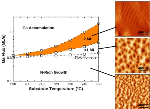
5.2 Influence of growth temperature and Ga flux ... 70
5.3 Conclusion ... 74
6. GaN/AlN heterostructures for the short-wavelength IR range ... 75
6.1 Ge vs Si doping in planar GaN/AlN heterostructures ... 75
6.1.1 Sample structure ... 75
6.1.2 Optical properties ... 77
6.1.3 Conclusion for Ge vs Si doping in planar GaN/AlN heterostructures ... 81
6.2 Ge vs Si doping in GaN/AlN nanowire heterostructures ... 81
6.2.1 Sample structure ... 82
6.2.2 Optical properties ... 85
6.2.3 Conclusion for Ge vs Si doping in nanowire GaN/AlN heterostructures ... 89
6.3 Top-down heterostructures ... 89
6.3.1 Sample structure ... 90
6.3.2 Optical properties ... 92
6.3.3 Conclusion for top-down heterostructures ... 95
6.5 General conclusions ... 95
7.2 Structural properties ... 98
7.3 Optical properties ... 101
7.4 Conclusion ... 106
8. Nonpolar heterostructures for the far-IR range ... 107
8.1 Sample design and growth ... 108
8.2 Structural characterization ... 110
8.3 Optical characterization ... 114
8.4 Conclusions ... 120
9. Single nanowire photodetectors ... 123
9.1 Quantum well infrared photodetector ... 123
9.1.1 Nanowire growth and device fabrication ... 124
9.1.2 Characterization and modeling ... 125
9.1.3 Device characterization ... 128
9.2 Single nanowire photodetectors for ultraviolet ... 133
9.2.1 Nanowire design, growth and device fabrication ... 134
9.2.3 Ultaviolet photoresponse ... 136
9.2.2 Simulations and discussions... 140
9.3 Conclusion ... 142
10. Conclusions and perspectives ... 145
10.1 Conclusions ... 145
10.1.1 Conclusions for the study of Ge as n-type dopant ... 145
10.1.2 Extension of ISB transition in GaN nanowires towards longer wavelengths ... 147
10.1.3 Top-down nanowires ... 147
10.1.4 Non-polar orientations to attain the FIR spectral region ... 147
10.1.5 Single nanowire photodetectors ... 148
10.2 Perspectives ... 149
References ... 151
Publications and conference contributions ... 171
1. Context and motivation
1.1 A brief history of infrared technology
The study of the distribution of radiant heat “across and outside” the visible solar spectrum with a set of thermometers by William Herschel almost 200 years ago resulted in the realization that there are rays invisible to the naked eye [1]. Since these rays were positioned outside the red part of the visible spectrum they were named infrared (IR) rays. The discovery of IR thermal emission at room temperature fueled the first applications as thermal imagers for the military. Night vision sensors, tank sight systems, heat seeking missiles were the immediate application of IR technology. At present, IR technology is widely used in many civil fields, such as remote temperature sensing, remote control, or short-range wireless communication. IR satellite images can now solve natural and economic problems. They can be used to understand the location of mineral deposits or the contents of forest or the state of a crop. IR imaging in medical diagnostics have also gained popularity recently.
Particularly interesting IR regions from the application viewpoint include the 1.3-1.55 µm wavelength window which is used for fiber optic communications [2], and the two atmospheric windows at 3-5 µm, for sensing hot objects (e.g. a flame or a jet engine), and at 8-14 µm, for high-performance thermal imaging around ambient temperature. There is an interest in even longer wavelengths for space applications [3]. The Terahertz range which roughly corresponds to the spectral region from 30 to 1000 µm (0.3 THz to 10 THz) is a non-ionizing radiation that appears as a harmless alternative to x-rays in medical, biological and security screening, and finds additional applications in high-speed wireless communication, industrial quality control, and spectroscopic imaging. There are various divisions for the IR spectrum depending upon applications. One of the most common is presented in Table 1.1.
Classification Wavelength range
Near IR 0.75 µm – 1.4 µm
Short-wavelength IR 1.4 µm - 3 µm
Mid-wavelength IR 3 µm - 8 µm
Long-wavelength IR 8 µm -15 µm
Far IR 15 µm – 1000 µm
Table. 1.1: Classification of IR wavelength spectrum
The most widely used IR device is the IR detector [4]. There are two classes of IR detectors, namely thermal detectors and photon detectors. In a thermal detector the incident radiation changes the temperature of the system, which results in a change in some measurable physical property. Examples of such detectors include the bolometer and the pyrometer. They have modest sensitivity and slow response. They are commercially successful because they are relatively cheap [3].
The second class of detectors, namely photon detectors, is largely related to the progress in the semiconductor industry. They rely normally on band-to-band transitions in semiconducting materials. Narrow bandgap materials like InSb, PbTe and PbS were initially used to make IR detectors. Later ternary alloys like III−V (InAs1–xSbx), IV−VI (Pb1–xSnxTe), and II−VI (Hg1–xCdxTe) were also introduced with the purpose of tuning the bandgap to improve the spectral response [4]. The Hg1–xCdxTe (HgCdTe) alloys might be the most successful materials for commercial IR photon detectors. The technology of HgCdTe has matured and produced a wide variety of detectors in different ranges over fifty years since the early sixties [5]. Later InGaAs alloys were attempted, like the In0.53Ga0.47As (Eg = 0.73 eV), lattice-matched
to InP, is an excellent detector material for the near−IR (1.0–1.7−μm) spectral range. However, the performance of InGaAs devices decreases rapidly if the alloy composition is varied due to lattice-mismatch-induced defects [4].
The introduction of quantum systems like quantum wells, quantum dots and nanowires provided an alternative solution to these problems. Esaki and Sakaki suggested that quantum confinement in GaAs/AlxGa1-xAs quantum wells (QWs) can be tuned to obtain intersubband (ISB) transitions [6]. The first experimental evidence of ISB absorption in a multi-QW (MQW) system was reported in 1985 by West and Eglash [7] followed by the fabrication of the first quantum well infrared photodetector (QWIP) in 1987 by Levine et al. [8]. In a QWIP, the quantum barrier height and quantum well width are crucial factors that decide the detectable wavelength band. In the last decade, QWIP cameras have undergone rapid development thanks to the standard manufacturing technology of GaAs, and they challenge HgCdTe alloy in the commercial scenario. QWIPs are characterized by fast response time and low power consumption. Current challenges in the QWIP technology include bringing up the operating temperature and extending their operation to shorter wavelength (less than 3 µm), which has been limited by material transparency and the available conduction band offset [2].
1.2 III-Nitride semiconductors
III-Nitride semiconductors (GaN, AlN, InN) are key materials for the development of optoelectronics and electronic devices in the 21st century thanks to their direct bandgap and doping capabilities. They are now extensively used in light emitting diodes (LEDs), which have revolutionized solid-state lightning. Nitride-based light emitters have also found applications in data storage, traffic lights, indoor agriculture etc. On the other hand, their high breakdown field and high electron mobility, combined with their mechanical and thermal robustness, makes them suitable candidates for high power electronics. AlGaN-based UV emitters for disinfection and water purification, and InGaN-based solar cells are currently under development.
III-Nitrides have also become interesting materials for infrared optoelectronics using intersubband transitions. In the late 90s, Suzuki et al. studied about the feasibility of the application of GaN based ISB technology for the telecommunication spectral range [9]. But
laboratories only in 1999 [10], where she demonstrated ISB transitions in the wavelength range 1.75 µm to 4.5 µm. She also made estimates of the ultrafast excited electron lifetime of GaN/AlN QWs [11]. It was not until 2003 that the first ISB photodetector based on III-nitrides was developed. Hofstetter et al. had fabricated a QWIP using GaN/AlN wells and they were able to measure the emission from a 1.55 µm superluminescent LED [12]. However, such a photoconductive QWIP displayed large dark current, originating from structural defects in the highly-mismatched GaN/AlN structures. The device was only able to operate up to 170 K.
An alternative to circumvent the leakage problem was found exploiting the device photovoltaic response, associated to the intrinsic asymmetry of the potential profile in polar GaN wells. The photovoltaic operation of GaN/AlN QWIPs at telecommunication wavelengths and at room temperature was first studied in detail by Hofstetter et al. [13–17]. These photovoltaic ISB detectors were based on resonant optical rectification processes [15,18]. In a GaN/AlN superlattice, due to the asymmetry of the potential in the QWs, the excitation of an electron into the upper quantized level is accompanied by a charge displacement in the growth direction, so that an electrical dipole moment is created. For a high electron density and a large number of QWs, these microscopic dipole moments can be detected as an external photovoltage. A strong enhancement of the responsivity has been achieved by using quantum dots (QDs) instead of QWs in the active region [19].
Another approach to reduce leakage is the quantum cascade detector (QCD), which consists of several periods of an active QW coupled to a short-period superlattice, which serves as extractor [20,21]. In contrast to QWIPs, they operate at zero bias. Under illumination, electrons from the ground state of the active QW, e1, are excited to the upper state, e2, and then transferred to the extractor region where they experience multiple relaxations towards the next active QW. Operated as photovoltaic detectors, their dark current is extremely low and the capacitance can be reduced by increasing the number of periods, which enables high frequency response.
The polarization induced electric fields of III-nitrides were put to use to develop efficient GaN/AlGaN QCDs in the near-IR region. For example, Vardi et al. in 2008 [22] demonstrated devices that operated in the near IR spectral range with a room temperature zero-bias responsivity of 10 mA/W at 1.7 µm. More recently, in 2013, Sakr et al. demonstrated a GaN/AlGaN waveguide QCD at λ = 1.55 µm with 40 GHz frequency bandwidth for 10×10 µm2 devices. They could obtain a peak response of 9.5±2 mA/W [23].
1.3 Semiconducting nanowires
In the last two decades, semiconducting nanowires have been widely studied due to the novel properties stemming from their low dimensionality. The first nanowire laser was demonstrated using ZnO [24] in 2001 and since then we have optically pumped coherent laser emission in nanowires who act as both waveguides for optical cavities and gain media for light amplification. Combining direct-gap III-V and II-VI nanowires with silicon nanowires and planar
silicon structures have produced multicolor electrically driven nanophotonic and integrated nanoelectronic-photonic systems [25]. Similar results were achieved using multi-quantum well (MQW) nanowire heterostructures, consisting of a GaN nanowire core that functions as the primary part of the optical cavity, and epitaxial InGaN/ GaN MQW shells that serve as the composition tunable gain medium [26].
In terms of photodetectors, the low electrical cross-section of nanowires implies low electrical capacitance, thus a larger operation bandwidth than planar devices. Owing to antenna effects, this comes without degradation of light absorption. Indeed, nanowire arrays can exhibit higher absorption than a thin film of the equivalent thickness [27]. The large surface-to-volume ratio allows misfit strain to be elastically released, which expands the possibilities for the active region design in terms of both size and composition. Also, the three-dimensional (3D) confinement of carriers in nanowire heterostructures might open new possibilities to control the carrier relaxation time [28,29].
The feasibility of electron transport via quantized levels in the conduction band of GaN/AlN heterostructured nanowires has been demonstrated by the fabrication of resonant tunneling diodes [30,31]. However, the field of nanowire ISB transitions is still in the nascent phase. Tanaka et al. [32] reported ISB absorption centered at 1.77 µm (= 0.7 eV) with a full width at half maximum (FWHM) of about 230 meV in a GaN/AlN (1 nm/2.7 nm) periodic heterostructure in GaN nanowires with the AlN barriers doped with Si at 2×1019 cm–3. In this configuration, it is assumed that the electrons from the donor levels in the AlN barriers should be transferred to the GaN nanodisks. Studies in GaN/AlN planar heterostructures indicate an improvement of the ISB absorption linewidth if the doping is performed directly in the GaN wells [33]. However, at the beginning of this PhD work, there was no report on ISB absorption in GaN/AlN nanowire heterostructures with Si-doped GaN nanodisks. Difficulties were attributed to the fact that Si dopants tend to degrade nanowire morphology and migrate towards the nanowire sidewalls, resulting in inefficient doping [34]. Replacing Si by Ge, Beeler
et al. [35] observed ISB absorption in GaN:Ge/AlN (4-8 nm /4 nm) heterostructures on GaN
nanowires, in the short-wavelength infrared region. The transitions were broad though, with a FWHM of 400 meV.
1.4 Motivation and targets
Using nanowires instead of planar heterostructures in ISB devices can lead to better performance due to lower electrical cross-sections. Also nanowires have generally diameters smaller than the wavelengths associated to their ISB transitions, and exhibit a large dielectric mismatch with the environment. The target of this work was to explore the possibilities of intersubband engineering GaN nanowires. With this purpose, on the one hand, we study
alternative dopants for better control of the morphology and carrier distribution, and on the
other hand, we try to extend this technology towards longer wavelengths. We systematically compare well-established planar designs with nanowire structures. We also explore the
alternative top-down approach for nanowire fabrication. The following is a summary of our
motivation for the various topics that are presented in this manuscript.
a) Alternative dopants
Silicon, the preferred n-type dopant for wurtzite GaN, contributes to edge type dislocation climb, leading to an increase in tensile stress [36–38]. Doping with Si in excess of 1019 cm–3 is reported to cause surface roughening and eventually crack propagation [37]. Ge, like Si, is a shallow donor in GaN, with a theoretical activation energy of 31.1 meV [39]. The ionic radius of a Ge atom is similar to that of Ga and the metal-nitrogen bond length changes by only 1.4% with Ge, compared to 5.5% with Si [40]. Hence Ge can occupy the Ga lattice site causing far less lattice distortion than other dopants. Also like Si, the DX- state of Ge is unstable and does not affect doping efficiency [40]. From both perspectives, fundamental and applied, it is important to perform extensive studies on Ge as a dopant in GaN.
There is also an interest to study Ge as a dopant in AlGaN. Gordon et al. [41] predicted that the onset of DX transition for Ge in AlGaN is at an Al content of 52%. They theoretically predicted that the DX configuration of Ge is more stable than that of Si (≈ 1 eV deeper into the bandgap), which is predicted to occur at 94% of Al content. However for Si, conductivity measurements suggest decreased conductivity at an Al content as low as 50% [42], which was attributed to shallow hydrogen like donor states. Experimental data was non-existent to verify theoretical predictions for Ge doped AlGaN.
To assess the interest of using Ge as a dopant in GaN intersubband devices, it is important to compare its performance in GaN/AlN heterostructures, both in the planar and in the nanowire geometry. While GaN based ISB devices have been demonstrated, they are primarily based on a planar geometry and utilize Si as a dopant. So based on the advancements in Ge doping in GaN thin films, it has become interesting to assess the performance of ISB structures as a function of the nature of the dopant, either Ge or Si. On the other hand, the first systematic study of ISB absorption in nanowires with doped quantum wells used Ge as n-type dopant in the already mentioned study by Beeler et al [35]. In that case, Ge-doped GaN/AlN (4–8 nm / 4 nm) heterostructures on GaN nanowires displayed ISB absorption in the short-wavelength infrared (SWIR) domain in the 1.3-1.95 µm range with broad transitions (FWHM of ≈ 400 meV). At the start of my PhD, there was no report on ISB absorption in GaN/AlN nanowire heterostructures with Si-doped GaN quantum wells.
b) Extension of the ISB transition in GaN/AlN nanowires towards longer wavelengths
At the beginning of my thesis work, ISB transitions in GaN/AlN nanowires had only been observed in the 1.3-1.95 µm range, in spite of using GaN wells as large as 8 nm [35]. This is explained by the dispersion introduced by irregularities in the well thickness and diameter along the growth axis. Thus, the absorption broadens, which reduces its peak intensity. In such a situation, higher doping levels are required to identify the ISB absorption, which leads to a blueshift of the transition due to many-body effects. It is therefore important to make an effort to improve the homogeneity of the nanowire along the growth direction in terms of diameter. Also important is uniformity from one nanowire to another along the substrate. This would ensure sharper absorption peaks and control of the heterostructure dimensions. Then,
the ISB transition can be shifted to longer wavelengths either by using larger quantum wells or by using AlGaN ternary alloys as quantum well barriers, thus reducing the internal electric field in the wells.
c) Top-down nanowires
Another approach to overcome inhomogeneities in the heterostructure dimensions consists in carefully performing top-down etching on planar heterostructures to create 3D arrays of micro/nano pillars. With III-As heterostructures, nano- and micropillar arrays for THz emission were demonstrated by lithographically defined top-down etching [43–45]. Such a process using GaN/AlN heterostructures had not been attempted at the beginning of this work.
d) Nonpolar orientations for far-infrared
The extension of the study of ISB transitions in nanowires towards the far-IR (FIR) was not possible due to time constraints. However, I have participated in the evaluation of nonpolar crystallographic orientations, particularly the m-plane, as an alternative to obtain GaN/AlGaN QWs without internal electric field [46–48]. We have shown that such structures can cover most of the 7–10 THz band inaccessible to GaAs based technologies.
e) Single nanowire photodetectors
The observation of ISB absorption in nanowire ensembles motivated us for the development of nanowire-based QWIPs. The first demonstration of such a device is presented in this manuscript.
1.5 Organization of the manuscript
Following these introductory pages, Chapter 2 starts with a brief summary of the general properties of III-nitride semiconductors, describing their crystal structure and their most relevant electronic, mechanical and optical features. Then, we present various semiconductor nanostructures and the appearance of subbands. Finally, we review the physics of ISB transitions and highlight the selection rules that govern these transitions and many-body effects that are to be considered.
Chapter 3 contains a description of the experimental methods and tools used in this work. Particular attention is paid to the description of plasma-assisted molecular beam epitaxy (PAMBE), the growth method used to synthesize all the samples described in this thesis.
In chapter 4, we present a study of Ge as an alternate n-type dopant, in place of Si, for wurtzite GaN and AlGaN thin films grown by PAMBE. We first prove that Ge does not introduce any perturbation in the GaN growth. We then analyze the effect of doping on the structural quality and estimate the Ge incorporation. We systematically assess the effect of Ge in electrical properties complemented by observing optical properties for various Ge doping concentrations and Al content in AlGaN.
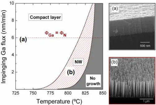
Chapter 5 describes the development of GaN nanowires grown by PAMBE. The insertion of a thin AlN buffer layer is necessary to improve the vertical alignment of the wires. However, the presence of AlN results in huge two-dimensional (2D) undergrowth. To solve this problem, we develop a low-temperature AlN growth process. We then make an analysis of the impact of the gallium flux and substrate temperature on the coalescence and growth rate of the nanowires.
In chapter 6, we present a study of GaN/AlN heterostructures designed to absorb in the SWIR spectral range. We assess both the effect of the nature of the n-type dopant, either Ge or Si, as well as the dopant concentration on the optical properties. We compare self-assembled nanowires and planar layers, and we also introduce heterostructures contained in top-down nano/micropillar arrays, and we study the effect of patterning on their ISB absorption.
Chapter 7 describes the GaN/(Al,Ga)N heterostructures in GaN nanowires structurally designed to absorb in the mid-wavelength infrared (MWIR) region. To shift the absorption to longer wavelengths, we follow two approaches, the first one increasing the GaN well width in GaN/AlN heterostructures from 1.5 to 5.7 nm, which leads to a redshift of the intersubband absorption from 1.4 to 3.4 µm. Through the second approach, we demonstrate intersubband absorption in GaN/Al0.4Ga0.6N heterostructures, thereby reducing the effects of polarization, which redshifts the intersubband transitions to cover the spectral range from 4.5 to 6.4 µm.
In chapter 8, we assess the possibility to observe ISB transitions in the 1.5–9 THz frequency range in nonpolar m-plane GaN/AlGaN MQWs, covering most of the 7–10 THz band inaccessible to GaAs based technologies. Such nonpolar structures present inhomogeneities of the Al composition in the barriers along the growth axis, however we did not identify any extended structural defects introduced by the epitaxial process. We study the effect of varying the Si doping concentration and we explore the use of Ge as a dopant.
In chapter 9, we present the first single-nanowire ISB photodetector (NW-QWIP), using GaN/AlN nanowire heterostructures that exhibit ISB transitions around 1.55 µm. In parallel, using band-to-band transitions, we report a single-nanowire UV photodetector incorporating an AlN/GaN/AlN heterostructure. Such a device presents a UV response that is linear with the optical power when the nanowire diameter is small enough to ensure a complete depletion of the wire.
Chapter 10 summarizes the accomplished work and main achievements, and considers its relevance and impact for future developments.
2. Introduction
2.1 Introduction to III-nitrides
2.1.1 Crystal structure
III-Nitride semiconductors like AlN, InN and GaN can appear in three crystalline configurations, namely wurtzite (α-phase), zinc blende (β-phase) and rock salt (-phase) structures. The wurtzite structure shows hexagonal symmetry with two hexagonal sublattices of metal (Al, Ga, In) and nitrogen (N) atoms which are shifted with respect to each other ideally by 3/8 [0001] (figure 2.1 (a)). The zinc-blende structure, also called sphalerite, shows a cubic symmetry, consisting of two interpenetrating face-centered cubic sublattices. One sublattice is shifted with respect to the other by ¼ [111] (figure 3.1 (b)). The rock salt structure, with a cubic symmetry where the two atom types form two interpenetrating face-centered cubic lattices, is the rarest configuration, appearing when crystals are synthesized under high pressure.
Figure 2.1: Schematic representation of (a) the wurtzite and (b) zinc-blende structures. The pink and violet spheres indicate metal and N atoms, respectively.
In this work, we focus on III-nitrides with wurtzite structure, which is the thermodynamically more stable configuration. I have used GaN as a reference for the discussion, unless described otherwise. Figure 2.1 (a) shows the a and c parameters of the hexagonal crystal structure of III-nitrides, and the anion-cation bond length u along the [0001] axis. A four index (h k i l) notation is used to refer to crystallographic planes or axis, which are described as a function of three base vectors a1, a2, a3 and the out-of-plane vector c, as presented in Figure 2.2. Note that i = -h-k, since the three base vectors are separated by an angle of 120°.
The family of basal planes is termed as {0001} c-plane. The c-plane orientation is the most commonly used in opto- and microelectronics. There are two other families of planes which are of high importance, namely the {1-100} m-plane and {11-20} a-plane, both perpendicular to the c-plane and containing an equal number of Ga and N atoms. These main crystal plane orientations in GaN are illustrated in figure 2.2.
Figure 2.2: Hexagonal structure of GaN with representations of the base vectors and main crystallographic planes.
Since the hexagonal lattice is not centrosymmetric, the [0001] and [000-1] directions are not equal. In the GaN bond perpendicular to the {0001} plane, the vector pointing from Ga to N is identified arbitrarily as the [0001] direction. If the material is grown along this direction then it is called Ga-polar if it is grown in the opposite direction then it is called N-polar.
In an ideal wurtzite crystal, the c/a and u/c ratios are 1.633 and 0.375, respectively. However, due to the difference in metal ions, the bond lengths and the resultant c/a ratios of AlN, GaN, and InN are different. Table 2.1 describes the lattice parameters of wurtzite III-nitrides at 300 K.
InN GaN AlN
c (Å) 5.703 5.185 4.982 a (Å) 3.545 3.189 3.112 c/a 1.608 1.626 1.6 u/c 0.377 0.377 0.382 References [49] [49,50] [49,50]
Table 2.1: Lattice parameters of bulk InN, GaN and AlN.
The knowledge of heteroepitaxy along the c-plane is well established. However, the growth in m- and a-plane orientations was not considered until recently due to the unavailability of suitable substrates. During the last decade, the realization of the importance of non-polar III-nitrides have first led to the fabrication of non-polar films/templates on foreign substrates. Few examples include a-plane GaN on r-plane sapphire substrates [51], or
m-plane GaN on m-plane SiC [52]. However, the heteroepitaxial growth on a and m-plane
layers is prone to high defect densities. More recently, halide vapor phase epitaxy (HVPE) has developed to the point of producing relatively thick (< 1 µm) GaN crystals along the [0001] direction [53], which can be diced into high-quality a- and m- plane platelets for epitaxy of nonpolar structures. The main drawback of this method, as of now, is the high cost involved and the limited surface area available for growth.
2.1.2 Band structure
The band structure of a semiconductor emerges as a solution of the Schrödinger equation of non-interacting electrons in the periodic lattice. Visualization of the bandgap requires a plot of energy vs. wavevector k = (kx, ky, kz). It is common to plot band structures as
curves of En(k) for values of k along straight lines connecting symmetry points in the k-space.
These points of symmetry occur in the first Brillouin zone and are labelled as Γ, Δ, Λ, Σ. The bandgap is described as the energy difference between the bottom of the conduction band and the top of the valence band. If the bottom of the conduction band and top of the valence band occur at the same symmetry point, then the material is said to have a direct bandgap. In the case of wurtzite III-nitrides, the bandgap is direct, with the conduction band minimum and the valence band maximum located at the Γ point. Due to the asymmetric nature of the wurtzite structure the valence band degeneracy is lifted. Thus the heavy hole (HH), light hole (LH) and spin-orbit, crystal field splitting (CH) subbands are separated as shown in the figure 2.3. The top of HH and LH subbands are higher than CH subband in energy for GaN. However, in the case of AlN the top of the CH subband is at higher energy than the HH or LH subbands.
Figure 2.3: Electronic structure of the valance band of (a) GaN and (b) AlN near the Brillouin zone centre point Γ for unstrained wurtzite material. For simplicity, zero energy is assigned to the top of the valence band.
The values of the bandgap of GaN, AlN and InN are summarized in table 2.2. An effective mass approximation can be utilized to describe the band structure at Γ(k=0) by assuming a parabolic band structure at this point. This means that the electron or hole behavior can be modelled as a free particle with an effective mass m* experiencing a fixed potential. Typical values of the effective masses for electrons and holes in III-nitrides are recorded in table 2.2. For ternary compounds like AlGaN or InGaN the bandgap is approximated by a quadratic equation:
𝐸𝑔(𝐴𝐵) = 𝑥𝐸𝑔(𝐴) + (1 − 𝑥)𝐸𝑔(𝐵) − 𝑥(1 − 𝑥)𝑏 (equation 2.1) where b is the bowing parameter, which accounts for the deviation from a linear interpolation between the two binaries A and B. The bowing parameter has a value of 0.8-1.3 eV in the case
of AlGaN [54]. By changing the Al or In content in GaN it is hence possible to obtain alloys with desirable bandgap. GaN AlN Eg (T = 0 K) (eV) 3.507 [55] 6.23 [55] αV (meV/K) 0.909 [55] 1.999 [55] βD (K) 830 [55] 1429 [55] m* e 0.2 m0 [56] (0.32-0.40) m0 [55,57] m* h 1.25 m0 [58] 1.44 m0 [59]
Table 2.2: Band parameters of GaN and AlN: bandgap energy at T = 0 K; Varshni parameters; electron and hole effective masses (m0 being the nominal mass in vacuum).
The bandgap of these materials is temperature dependent due to electron-lattice interactions and temperature dependence of the lattice parameters [60,61]. The temperature variation of the bandgap can be estimated by using the Varshni equation:
Eg(T) = Eg(T = 0 K) −αVT2
βD+T (equation 2.2) where αV and βD are the Varshni and Debye coefficients respectively, whose values for GaN
and AlN are listed in Table 2.2.
2.1.3 Elastic properties
Strain is introduced during the epitaxial growth because of the mismatch of lattice constants and thermal expansion coefficients with the substrate. Strain affects the optical, electrical and bandgap properties of the III-nitrides.
In the framework of linear elasticity, Hooke’s law describes the relation between the stress (σij) applied to a material and the strain (kl):
σij = ∑Cijkl kl (equation 2.3) where (Cijkl) is the fourth-order elastic tensor. For simplification, we introduce the indices {1,2,3,4,5,6}, which replace the pairs of indices {xx,yy,zz,yz,zx,xy}:
1 = xx ; 2 = yy ; 3 = zz 4 = yz , zy ; 5 = zx , xz ; 6 = xy , yx
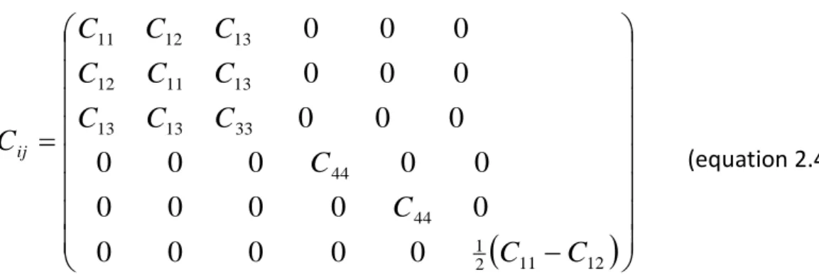
The elastic module can be represented by a matrix (a second-order tensor). For a crystal of hexagonal symmetry, this matrix contains six elastic modules, of which five are independent, as given in equation (2.4):
12 11 2 1 44 44 33 13 13 13 11 12 13 12 110
0
0
0
0
0
0
0
0
0
0
0
0
0
0
0
0
0
0
0
0
0
0
0
C
C
C
C
C
C
C
C
C
C
C
C
C
C
ij (equation 2.4)Calculated and experimental values of the parameters Cij for InN, GaN and AlN are summarized in table 2.3. C11 C12 C13 C33 C44 References InN 271 124 94 200 46 [62] theory 223 115 92 224 48 [63] theory GaN 374 106 70 379 101 [64] exp. 390 145 106 398 105 [65] exp. 365 135 114 381 109 [66] exp. 370 145 110 390 90 [67] exp. 396 144 100 392 91 [62] theory 367 135 103 405 95 [63] theory AlN 411 149 99 389 125 [68] exp. 410 140 100 390 120 [67] exp. 398 140 127 382 96 [62] theory 396 137 108 373 116 [63] theory
Table 2.3: Experimental and theoretical stiffness constants of InN, GaN and AlN in GPa.
During heteroepitaxy of thin films of III-nitrides on the (0001) plane, the in-plane stress is uniform (σ11 = σ22 = σ) and there is no stress along the c axis or shear stress (biaxial stress configuration). In this case, the Hooke law is simplified as in equation (2.5).
3 2 1 33 13 13 13 11 12 13 12 11 0 C C C C C C C C C (equation 2.5)
Therefore, in such a situation, the strain components 1 and 2 are equal and their value is given by:
ε1 = ε2 = εxx = - (aepi - asub)/asub (equation 2.6)
where aepi and asub are the lattice constants of the epilayer and the substrate, respectively.
The biaxial strain induces a strain ε3 of opposite sign along the [0001] axis perpendicular to the surface given by:
ε3 = εzz
=
-2(C13/C33) εxx (equation 2.7)2.1.4 Polarization effects in III-nitrides
A prominent feature among III-nitrides is the presence of strong polarization in the crystal. Since nitrogen atoms are more electronegative than metal atoms, the cation-N bonds can be considered as an electrostatic dipole. Due to the lack of symmetry of the wurtzite structure, this charge distribution is not fully compensated along the [0001] direction, which leads to spontaneous polarization Psp.. The values of spontaneous polarization for III-nitride
materials are described in table 2.4.
GaN AlN InN Ref.
Psp (C/m2) -0.029 -0.081 -0.032 [69]
Psp (C/m2) -0.032 -0.100 -0.041 [70]
Table 2.4: Calculated spontaneous polarization for wurtzite type GaN, AlN and InN.
If stress is applied to the III-nitride lattice, the lattice parameters c and a of the crystal structure will be changed to accommodate the stress. Thus, the polarization strength will be changed. This additional polarization in strained crystals is called piezoelectric polarization. The piezoelectric polarization in wurtzite III-nitrides can be calculated with the following equation: xy xz yz zz yy xx e e e e e 0 0 0 0 0 0 0 0 0 0 0 0 0 P 33 31 31 15 15 PZ (equation 2.8)
where eij are the piezoelectric coefficient of the material and j is the stress tensor. The piezoelectric polarization constants for InN, GaN and AlN are indicated in table 2.5.
e33 (C/m2) e31 (C/m2) e15 (C/m2)
InN 0.97 -0.57 -
GaN 0.73 -0.49 -0.30
AlN 1.46 -0.60 -0.48
Ref. [69] [69] [71]
2.2 Introduction to semiconductor nanostructures
The advancement in epitaxial deposition techniques allowed the fabrication of heterostructures. Figure 2.4 shows the three possibilities of alignment of bandgap minima along the growth direction depending on the band offsets, known as type I, II and III. The idea can be taken further to produce heterostructures like QWs (figure 2.5), where quantified electron levels appear as a result of the quantum confinement.
Figure 2.4: Description of the band edge profile at heterojunctions.
Figure 2.5: Simplified model of quantization of energy levels of a particle in a QW with finite barriers (modified from ref. [72]).
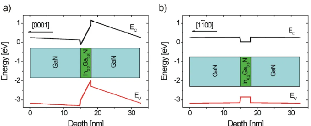
In III-nitrides, heterostructures are always type I. The conduction band offset in the GaN/AlN system is around 1.8 eV [73]. The discontinuity of the polarization vector at a heterointerface results in a fixed charge sheet at the interface, which can induce accumulation or depletion of free carriers. This fixed charge sheet generates an internal electric field in nanostructures, which is maximum for growth along the <0001> axis, where it can reach several MV/cm. In (0001)-oriented QWs, the internal electric field generates a band bending as seen in figure 2.6 (a). This leads to a spatial separation of electron and hole wave functions along the growth axis, which results in the so-called quantum confined Stark effect (QCSE). This means that the band-to-band transition is shifted to lower energy and the radiative lifetime increases due to the reduced electron-hole wave function overlap.
Figure 2.6: Band edge profile for an InGaN QW with GaN barrier interface in (a) c-plane growth (b) m-plane growth.
In the case of heterostructures grown on the m-plane or on the a-plane, the polarization dipoles are perpendicular to the direction of growth. Therefore, there is no polarization discontinuity at the heterostructure interfaces along the growth direction. Hence these are called non-polar orientations or non-polar directions [74]. The band structure of a QW presents a square profile, as described in figure 2.6 (b).
Various nanostructures like QWs, nanowires, or QDs have been widely studied. These are basically differentiated based on the number of dimensions in the volume of the object with nanoscale size. A detailed description of the calculation of their band structure can be found in ref. [75]. A simple description of the results is mentioned here to guide the reader to the difference between QW structures and nanowire-based QWs, which are essentially quantum dots if the nanowire radius is small enough to provide 3D confinement. Nevertheless, exact calculation of states needs the contribution of all 3 degrees of confinement even at large radius (typically 40-80 nm in our case).
The energy of an electron in a QW with confinement in x-direction can be written as
𝐸2𝐷 = 𝐸𝑛𝑥+ 𝑝𝑦2+𝑝𝑧2
2𝑚∗ (equation 2.9) where 𝐸𝑛𝑥 is the energy of the nth level of quantized motion in the x-direction. The electrons in such nth state can have total energy 𝐸
𝑛 ≤ 𝐸 < ∞. This set of quantum states for the given n is usually called the subband of dimensional quantization.
In the case of the nanowire grown along the z-direction, with confinement in x- and y- direction, the energy of the electron can be written similarly as,
𝐸1𝐷= 𝐸𝑛𝑥,𝑛𝑦+ 𝑝𝑧2
2𝑚∗ (equation 2.10) The nanowires also form similar subband quantization. The momentum dependence on the total energy of the electron is described in figure 2.7 (a, b) for 2D and 1D confinement.
In the case of a cubic quantum dot with confinement in x-, y- and z- directions, the total energy is a constant depending on the quantum numbers nx, ny and nz.