HAL Id: tel-03103308
https://tel.archives-ouvertes.fr/tel-03103308
Submitted on 8 Jan 2021
HAL is a multi-disciplinary open access archive for the deposit and dissemination of sci-entific research documents, whether they are pub-lished or not. The documents may come from teaching and research institutions in France or abroad, or from public or private research centers.
L’archive ouverte pluridisciplinaire HAL, est destinée au dépôt et à la diffusion de documents scientifiques de niveau recherche, publiés ou non, émanant des établissements d’enseignement et de recherche français ou étrangers, des laboratoires publics ou privés.
Investigation of resistive memories for Storage Class
Memory applications
Diego Alfaro Robayo
To cite this version:
Diego Alfaro Robayo. Investigation of resistive memories for Storage Class Memory applications. Micro and nanotechnologies/Microelectronics. Université Grenoble Alpes [2020-..], 2020. English. �NNT : 2020GRALT036�. �tel-03103308�
THÈSE
Pour obtenir le grade de
DOCTEUR DE L’UNIVERSITÉ GRENOBLE ALPES
Spécialité : NANO ELECTRONIQUE ET NANO TECHNOLOGIES Arrêté ministériel : 25 mai 2016
Présentée par
Diego ALFARO ROBAYO
Thèse dirigée par Gerard GHIBAUDO, Directeur de Recherche, Université Grenoble Alpes
et codirigée par Gabriel MOLAS, CEA
préparée au sein du Laboratoire CEA/LETI
dans l'École Doctorale Electronique, Electrotechnique, Automatique, Traitement du Signal (EEATS)
Mémoires resistives pour applications
Storage Class Memory (SCM)
Investigation of resistive memories for
Storage Class Memory applications
Thèse soutenue publiquement le 22 septembre 2020, devant le jury composé de :
Monsieur AHMAD BSIESY
PROFESSEUR DES UNIVERSITES, UNIVERSITE GRENOBLE ALPES, Président
Monsieur QUENTIN RAFHAY
MAITRE DE CONFERENCES HDR, GRENOBLE INP, Examinateur
Madame MARIE-PAULE BESLAND
DIRECTRICE DE RECHERCHE, CNRS DELEGATION BRETAGNE PAYS DE LOIRE, Rapportrice
Monsieur PAOLO PAVAN
PROFESSEUR , UNIV. DE MODENE (REGGIO EMILIE) - ITALIE, Rapporteur
Monsieur DAMIEN DELERUYELLE
Abstract
Investigation of Resistive Memories (ReRAM) for
Storage Class Memory applications (SCM)
In classical von-Neumann architectures, processing and memory blocks are separated. Latency times for the latter are much more slower. To boost performances, memory hier-archy has been introduced to combine small, fast, but expensive technologies with large, slower, and cheaper ones. In such hierarchy, a notorious latency and storage gap can be distinguished between the lowest memory level and the highest storage one: DRAM and Flash blocks, respectively. Emerging non-volatile technologies are called to fill such gap through the so-called Storage Class Memories (SCM). Among them, Resistive Random-Access Memories (ReRAM), represent an interesting candidate to improve flash perfor-mances due to their good scalability, low-power consumption, Back-End of Line compati-bility, fast writing and erasing process, and good endurance. However, several roadblocks hinder their implementation at large industrial scale, notably high variability, and low non-linearity, which avoids large crossbar arrays implementation. This thesis work ex-plores such aspects to increase attractiveness of ReRAM technologies for SCM applica-tions. For the former, endurance variability is addressed at the array level through various measurements over diverse stacks configurations. Results allow to study the impact of programming conditions on failure mechanisms dispersions, leading to the development of a stochastic model based on defects generation inside the resistive layer. As for the non-linearity issue, successful co-integration between best-in-class HfO2 and GeSeSbN
Ovonic Threshold Selector (OTS) in 1S1R structures, is demonstrated. Hence, leakage currents compatible with 100Mb-1Gb bank size are obtained. For the first time, to our knowledge, key parameters of OTS+ReRAM systems for high-density crossbar arrays are identified and studied at the statistical level, allowing proposition of further optimizations and opening the way to a whole field of studies which include new materials and circuits to improve 1S1R performances.
Keywords: Resistive Random Access Memories (ReRAM); OxRAM; CBRAM; Ovonic
Résumé
Mémoires résistives pour applications
Storage Class Memory (SCM)
Dans les architectures classiques dites de Von-Neumann pour des systèmes d’information, les blocs de mémoire et de traitement sont séparés. Pour le premier, les temps d’accès sont beaucoup plus importants. Afin d’optimiser les performances, une hiérarchie de mémoire a été mise en place. Elle combine des technologies coûteuses, de petite taille, mais très performantes en termes de vitesse; avec d’autres plus larges, à bas coûts per bit, mais plus lentes. Dans une telle hiérarchie, un gap important existe en termes de temps d’accès et capacité de stockage entre les blocs de mémoire les plus bas et ceux de stockage les plus hauts (briques DRAM et FLASH, respectivement). Des technologies émergentes non-volatiles, appelées Storage Class Memories (SCM) sont candidates à rem-plir tel gap. Entre elles, les mémoires résistives vives, ReRAM, de l’abbreviation anglaise pour Resistive Random Access Memories; représentent une alternative très intéressante grâce à leur bonne scalabilité, basse consommation, compatibilité avec la Back-End-Of-Line (BEOL), leurs temps d’écriture et lecture rapides, ainsi qu’une bonne endurance. Cependant, plusieurs obstacles empêchent leur implémentation à l’échelle industriel, no-tamment la haute variabilité des états résistifs et la non-linéarité réduite entre eux, ce qui limite l’implémentation des matrices mémoires larges. Ces deux aspects sont étudiés dans ces travaux de thèse. Pour la variabilité, il se trouve que l’endurance, caractéristique fon-damentale vis-à-vis des applications SCM, est aussi dispersée. Ce manuscrit présente des caractérisations électriques en endurance au niveau statistique sur des matrices ReRAM de 4Kb. Plusieurs empilements mémoires furent étudiés, ainsi qu’une grande variété des conditions de programmation pour le cyclage. Il a été observé comment la valeur médi-ane et la déviation standard du claquage des mémoires sont principalement affectées par le RESET. Les résultats expérimentaux ont été utilisés dans la proposition d’un modèle stochastique basé sur la génération de défauts dans la couche résistive. Concernant l’autre grand axe de cette thèse, une co-intégration réussie entre une mémoire HfO2 (1R) et un
sélecteur (1S) de type Ovonic Threshold Switch (OTS), a été demontrée. Les courants de fuite, obtenus grâce à l’addition de l’OTS, sont compatibles avec des matrices entre 100Mb et 1Gb. Pour la première fois, à notre connaissance, des paramètres influant sur les performances des structures 1S1R ont été étudiés au niveau statistique pour des matrices crossbar à haute densité, ainsi permettant la proposition d’optimisations futures et des nouvelles études incluant des nouveaux matériaux et circuits, pour continuer à améliorer les performances des dispositifs 1S1R.
Mots clés: Mémoires vives résistives (ReRAM); OxRAM; CBRAM; sélecteurs OTS;
Acknowledgments
"This is the end, beautiful friend. This is the end, my only friend. The end...", we hear that piece of "The End" by The Doors, while a military helicopter crosses the screen with a tropical forest burning in the background. This scene, appearing in the Francis Ford Coppola film, Apocalypse Now; is part of one of the most enjoyable sequences in cinema history. At least for me, it remains as a vivid memory and just now, while I am writing this acknowledgments section, it is playing in my head. I am not sure why. Maybe because they mark the final stage of this writing journey that has been the PhD manuscript. Even if it comes as the very last step, I consider saying thank you one of the most important aspects in life, so here we go.
First, I would like to thank Gérard Ghibaudo for being my thesis director and for enlightening the path with his immense knowledge during the darkest hours. Thanks to Quentin Rafhay for his enormous help and his guidance in key moments of this thesis. His ideas were always important to keep the pace for the progress of the subject.
Thank you Gabriel Molas. I am glad with life for finding not only a supervisor but also a person with great human quality. He was able to motivate me to give my best, while being patient and he cheered me up when things got complicated. All our discussions were very fruitful and I learned from his professionalism in countless aspects.
Being the young padawan of Cécile Nail and Gilbert Sassine was an easy job. Thanks to them for the time they dedicated to teach me their best skills in the lab and for letting me help them with their research when I was just and apprentice in the advanced electronics memories field. Anthonin Verdy was also my mentor for the Ovonic Threshold Selector part. I thank him for his advice and help with such devices and with the chalcogenide materials in general. In addition, I want to mention Joel Minguet, who became an amazing partner for the OTS+RRAM studies. Thank you for your help and knowledge Joellio.
Obtaining the most remarkable results of this thesis work would not had been possible without the help of incredible researchers, whom I met during these three years at CEA-Leti: Laurent Grenouillet, Gabriele Navarro, Elisa Vianello, Jean-François Nodin, Eti-enne Nowak, Cathy Carabasse, Niccolo Castellani, Carlo Cagli, Jacques Cluzel, Lorenzo Ciampolini, and Bastien Giraud. Thanks to Damien Deleruyelle from the INL Lyon for his outstanding help with the modeling sections.
As Sean Bean would say: "One does not simply fight bureaucracy". I would add that without help and righteous orientation, you are lost. This is why I am deeply grateful to Sabine Revol and Brigitte Gaillard. Their good energy and mood always gives you a reason to smile.
of interns, PhD students and Post-Docs in our lab. Thanks to all of them for sharing valuable moments and experiences with me.
I do not want to finish without thanking the latino gang in Grenoble. They are mi family here in France and those one understanding most of my silly jokes during countless meetings. Special mention goes to: Diana, Leo, Javi, Tomas, Gus, Andre, Carolina, Jorge, Javi, Odens, and Mi Reay. Aguante!!.
Furthermore, thanks to my family for all their support. They gave me strength and a lot of love during this thesis. All the experiences and moments lived, as well as the people I met during all these years in France are thanks to them. Last but not least, thanks a lot to Kathy who accompanied me for most of the thesis, and especially during the anxiogenic experience that was the coronavirus lockdown, when most of the writing took place. She will never forgive me for not knowing who Jose Barros was, paila, bu that is life.
I think now I understand why that scene of Apocalypse Now was playing in my head. If you have watched the film, you will know it is part of the opening sequence. Legend goes that Francis Ford Coppola was drinking and his brain was racking as he was searching a prologue for the movie, and at some point, the answer became clear: best openings begin with an ending. I am sure the conclusion of these thesis work will be the starting point for many more interesting and exciting things to come. Thank you all.
"... So it’s yerba and nails. What do you want the nails for?" "I’m not sure yet," Oliveira said, confused. "Actually, I took down the can of nails and found they were all twisted. I started to straighten them out, but with all this cold, you see... It’s my idea that as long as I have straight nails I’ll know what to use them for." -Hopscotch, Julio Cortazar, Chapter 41. Translation by Gregory Rabasssa and Paul Blackburn.
Contents
Abstract ii Acknowledgments v Outline xvi 1 Introduction 1 1.1 Memory Context: . . . 31.2 Storage Class Memories: a new paradigm . . . 5
1.3 Non-volatile Memories: emerging technologies for SCM applications . . . . 6
1.3.1 MRAM . . . 7
1.3.2 FeRAM . . . 8
1.3.3 PCRAM . . . 9
1.3.4 Mott-Insulators based memories . . . 11
1.3.5 Resistive Random Access Memories . . . 11
1.3.5.a ReRAM classification . . . 12
1.3.5.b Conduction models and working mechanisms of ReRAM technologies . . . 15
1.4 SCM: a new memory market . . . 19
1.5 3D Architectures . . . 21
1.5.1 Sneak path current in 3D Architectures . . . 22
1.6 Selector devices for crosspoint three-dimensional systems . . . 24
1.6.1 Si based . . . 25
1.6.2 Oxide tunnel barrier . . . 26
1.6.3 Mixed Ionic Electronic Conduction (MIEC) . . . 26
1.6.5 Threshold switching . . . 31
1.7 Emerging memory technologies and selector devices: benchmark . . . 34
1.7.1 SCM device candidates: comparison . . . 35
1.7.2 ReRAM for SCM applications . . . 36
1.7.3 Resistive memories for low-power applications and non-von-Neumann architectures . . . 37
1.7.4 Selectors benchmark . . . 39
1.7.5 OTS devices for crossbar arrays . . . 40
References . . . 41
2 Studied Devices and Measurement Methods 55 2.1 Studied Devices . . . 56
2.1.1 ReRAM devices . . . 56
2.1.2 OTS devices . . . 57
2.1.3 OTS+OxRAM structures . . . 58
2.2 Stacks architectures and structures . . . 58
2.2.1 IRMA mask . . . 59
2.2.1.a VIA structure . . . 59
2.2.1.b MESA structure . . . 60
2.2.2 Memory Advanced Demonstrator (MAD) test vehicle . . . 60
2.2.2.a Matrix Arrays . . . 61
2.3 Experimental methodology . . . 63
2.3.1 Measurement types . . . 63
2.3.1.a Quasi-static programming . . . 63
2.3.1.b Pulsed programming . . . 64
2.3.1.c Staircase programming . . . 65
2.3.2 Testbenches setup . . . 65
2.3.2.a Single devices . . . 65
2.3.2.b Matrix arrays . . . 66
2.4 Main metrics of the devices under test . . . 67
References . . . 70
3.1 A general overview of ReRAM variability and failure mechanisms produced
by programming cycling . . . 75
3.1.1 ReRAM variability . . . 75
3.1.2 Endurance failure mechanisms of ReRAM . . . 79
3.2 Technological details . . . 80
3.3 Experimental Results . . . 81
3.3.1 Maximum Endurance Statistics and Hard Breakdown Evidence . . 82
3.3.2 Ncmax statistics as a function of the applied programming conditions 85 3.3.3 Gradual Degradation Phenomenon . . . 88
3.4 Numerical Model . . . 89
3.4.1 Geometrical considerations: constriction size and shape . . . 91
3.4.2 Probability law considerations . . . 92
3.4.3 Fitting of experimental results . . . 94
3.5 Conclusions and Perspectives . . . 96
References . . . 98
4 Co-Integration of OTS+OxRAM memory for crosspoint arrays 103 4.1 OTS: general considerations and working principle . . . 105
4.1.1 Physical working mechanism of OTS selectors . . . 106
4.2 OTS devices for 3D crosspoint arrays . . . 110
4.3 OTS optimization . . . 113
4.3.1 Se-rich Ge-Se based OTS devices: doping effects . . . 114
4.3.2 GSSN thickness: influence over electrical performances . . . 115
4.3.3 OTS: thermal considerations . . . 116
4.4 ReRAM+OTS co-integration . . . 117
4.4.1 Technological details . . . 117
4.4.2 ReRAM+OTS switching . . . 118
4.4.3 Reading scheme . . . 119
4.4.4 Reading margin evolution with thickness and influence over OxRAM resistive states . . . 122
4.4.5 Pulsed mode operation of 1S1R devices . . . 123
4.4.6 Temperature Stability . . . 126
4.5.1 Bias Schemes . . . 128
4.5.2 Size estimations based on sensing limit features of periphery circuits 129 4.5.3 Size estimations limited by IR drop and periphery circuits . . . 130
4.6 Conclusions and Perspectives . . . 134
References . . . 135
5 OTS+OxRAM Variability and Reliability Studies 141 5.1 Technological Details . . . 142
5.2 1S1R working mechanism and switching characteristics: short recall . . . . 143
5.3 ON state characteristics of 1S1R systems . . . 144
5.4 Device performances and reliability studies . . . 146
5.4.1 Current Margin at VRead . . . 148
5.4.2 Selectivity . . . 148
5.4.3 Voltage Reading Margin (RM) . . . 149
5.5 Simulations and Discussion . . . 153
5.5.1 Influence of OxRAM variability over 1S1R performances and device optimizations . . . 153
5.5.2 Semi-analytical statistical analysis of 1S1R threshold switching based on Metastable Nucleation Filament Model (MNFM) theory (1) . . . 157
5.5.2.a Model results . . . 161
5.6 Conclusions and Perspectives . . . 164
References . . . 166
6 General Conclusions and Perspectives 170 6.1 Conclusions . . . 170
6.2 Perspectives . . . 171
7 List of Publications 173
(1)This model is a collaboration with Prof. Damien Deleruyelle from the Nanotechnologies Institute
List of Figures
1.1 Annual size evolution of Internet data. . . 2 1.2 Typical memory hierarchy in a Von Neumann architecture. . . 4 1.3 Approximative market shares in 2016 for Stand-Alone and embedded applications. 5 1.4 Memory hierarchy in terms of storage capacity and latency speed. . . 6 1.5 MRAM device example and resistive electrical behavior. . . 8 1.6 FeRAM basic structure and polarization behavior as a function of the applied
electric field . . . 9 1.7 Basic structure of PCM memories and typical IV curve showing the contrast
between the crystalline (high conductive) and amorphous (low conductivity) states. 10 1.8 Basic structure of a ReRAM cell as well as the IV curve for unipolar and bipolar
behaviors. . . 13 1.9 SET and RESET processes for CBRAM devices. . . 15 1.10 Schematic process of the switching mechanism in oxide-based RAM (OxRAM)
devices . . . 16 1.11 Types of conduction mechanisms taking place inside dielectric films which include
ReRAM memories. . . 18 1.12 Possible conduction mechanisms taking place inside resistive memories . . . 18 1.13 Switching behavior of ReRAM devices and RON resistance dependence on the
programming current. . . 20 1.14 Schematics of a 3D crosspoint and vertical ReRAM(ReRAM) . . . 22 1.15 3D X-Point (read crosspoint) technology presented by Intel/Micron in 2015. . . . 23 1.16 Cross-section and electrical behavior of a typical NPN configuration used as access
devices . . . 27 1.17 Band diagram for a single layer tunnel barrier made of SiNx . . . 28
1.18 Example of IV characteristic for a multilayer (T a2O5/T aOx/T iO2) oxide-based
access device . . . 28 1.19 Mixed Ionic Electronic Conduction (MIEC) selectors. Schematic and IV
1.20 Schematic view and IV characteristic for a tpypical Complementary Resistive
Switch configuration (CRS) . . . 31
1.21 IV characteristic of a Metal Insulator Transition (MIT) selector device. . . 32
1.22 IV characteristic of a Field Assisted Superlinear Threshold (FAST) for various layer thicknesses. . . 34
1.23 Example of IV behavior for an Ovonic Threshold Switching (OTS) selector . . . 35
1.24 Resistive Random Access Memories (ReRAM), maturity curve . . . 38
2.1 ReRAM stacks studied in this work. . . 57
2.2 OTS stack studied in this thesis. . . 57
2.3 OTS+ReRAM stack . . . 58
2.4 Contact Scheme of the CEA-Leti’s IRMA test vehicle for a tested device. . . 59
2.5 Schematic view of VIA and MESA structures used to integrated the tested devices over the IRMA test vehicle. . . 60
2.6 Schematic cross-section of the Memory Advanced Demonstrator (MAD) test vehicle 61 2.7 Matrix arrays on MAD test vehicle and pads structure. . . 62
2.8 Quasi-static programming regime. Example of IV characteristic and reading methodology for a ReRAM device. . . 64
2.9 Pulsed programming schematics. . . 65
2.10 Single devices testbench . . . 66
2.11 Testbench for Matrix Array characterization . . . 67
2.12 Endurance example for a ReRAM stack . . . 68
2.13 Retention test example for a ReRAM stack with failure time extraction. . . 69
3.1 Summary of main industrial demonstrators for PCM, STT-RAM and ReRAM technologies. . . 74
3.2 Forming voltage dispersions as a function of the device size for HfOx 5 and 10 nm thick. . . 76
3.3 HRS and LRS cumulative distributions for diverse compliance currents for a typ-ical OxRAM stack. . . 77
3.4 Standard deviation (σR) as a function of the median value (µR). . . 78
3.5 Endurance failure mechanisms. . . 80
3.6 (a). TEM cross sections and schematics for the studied stacks (CBRAM Al2O3/CuT ex, OxRAM HfO2/T i). (b). Schematic of the 1T1R structure used in this work. . . 81
3.7 Typical endurance curves for CBRAM and OxRAM stacks used for this work. . . 83
3.8 Extracted distribution of the maximum number of cycles for the endurance mea-surement from Figure 3.7 . . . 84
3.9 Measured maximum endurance distributions for CBRAM and OxRAM stacks for
diverse programming conditions and oxide thicknesses. . . 84
3.10 SET voltage influence over Ncmax distributions. . . 86
3.11 RESET voltage influence over Ncmax distributions. . . 87
3.12 Window Margin (WM) and maximum endurance dependence for various SET and RESET conditions . . . 88
3.13 Median values of the switching voltage and Rof f evolution during endurance using a RVS method to extract the Vswitch for a CBRAM stack. Gradual degradation in the dielectric is showed. It means that generation of the filament is easier with cycling. . . 89
3.14 Correlation between Rof f and Vswitch. . . 90
3.15 Schematics of Ncmax stochasti model. . . 91
3.16 Filament geometry and shape influence on the Ncmax dispersions using the nu-merical model. . . 93
3.17 Probability law comparisons. . . 94
3.18 Experimental and simulated Ncmax distributions for Al2O3/CuT ex CBRAM for two different programming conditions. . . 95
4.1 Typical current voltage characteristics for an OTS selector. . . 106
4.2 Metavalent bonding model. Density of States (DOS) and amorphous structure results. . . 108
4.3 Metavalent bonding model. Pair distribution functions (PDF)for GS and GSSN alloys before, during and after electrical stimulus . . . 109
4.5 1S1R main integration steps . . . 112
4.8 Sb content influence over GSSN electrical performances . . . 115
4.9 OTS thickness influence over GSSN electrical performances . . . 116
4.10 SEM. TEM EDX and HAADF cross sections for the 1S1R devices . . . 117
4.11 Superposed IV curve OTS and ReRAM devices . . . 118
4.12 Typical IV characteristics of the co-integrated 1S1R device. . . 119
4.13 1S1R reading strategies . . . 120
4.14 ∆Vth reading strategy with its main metrics specified. . . 122
4.15 Main 1S1R key metrics distributions. . . 123
4.16 Impact of GSSN thickness over the threshold switching voltages of the 1S1R devices.124 4.17 Window margin for a HfO2 stack and IV characteristic example . . . 124
4.18 Pulsed mode operation of 1S1R devices: SET and RESET pulses . . . 125
4.20 Temperature stability of OTS+ReRAM systems . . . 127
4.22 Array size estimation based on Ileakage measurements. . . 130
4.23 Physical schematic of a crosspoint array with dimensions used for IR drop esti-mations. . . 131
4.24 Bank size estimations based on IR drop and periphery circuitry considerations . 133 5.1 SEM, EDX and TEM cross sections for the 1S1R devices. . . 143
5.2 IV characteristics for 1S1R devices for a 15nm GSSN thickness and a 10nm HfO2 OxRAM . . . 144
5.3 Impact of the programming current on the ON state resistance for OTS, OxRAM and OxRAM+OTS structures. . . 146
5.4 ON state resistance evolution of OTS and OxRAM devices, prior to stabilization. 146 5.5 Representation of the three key features identified over 1S1R structures, and based on electrical behaviors, aiming to have highly reliable crosspoint arrays. . . 147
5.6 Current margin measurements for both 15 and 25nm GSSN thicknesses . . . 148
5.7 Selectivity measurements for both 15 and 25nm GSSN thicknesses . . . 149
5.8 Endurance tests over 1S1R structures with 15nm GSSN . . . 150
5.9 Cycle to cycle evolution of Vth1 and Vth2 for 1S1R devices. . . 151
5.10 Vth1 and Vth2 distributions using staircases pulses. . . 152
5.11 Vth1 distributions comparison for both 15 and 25nm GSSN as well as cycle to cycle and device to device dispersions for the 25nm GSSN. . . 152
5.12 Poole-frenkel conduction model to determine OxRAM resistive states over 1S1R performances. . . 154
5.13 Voltage drop dispersion using HRS distribution and a Poole-Frenkel regime . . . 155
5.14 Estimation of Vth1 dispersion using HRS typical distribution and Poole-Frenkel conduction regimes for the IV characteristic of the OxRAM values. Several ReRAM technologies are studied. . . 156
5.15 Measured Vth1 and Vth2 with various GSSN thicknesses with HRS estimations using V th2, median vales for every thickness. . . 156
5.17 Nucleation of a crystal nucleus and growth observed through a laser beam . . . . 158 5.18 Schematic view of the semi-analytical model using a field induced nucleation theory.159
Outline
This thesis was a collaboration between the IMEP-LAHC and the CEA-Leti. The main objective was to evaluate performances of Resistive Random Access Memories (ReRAM) for Storage Class Memory (SCM) applications through in depth characterization and modeling studies. In particular, speed, endurance and consumption were addressed with an additional focus on access device co-integration, also called selector.
Chapter 1 presents a general introduction to the context and motivation that led to do this research work. Basic concepts and main emerging memory technologies as well as selector topologies are presented. Main challenges of these devices regarding SCM applications are also treated.
Chapter 2 describes the studied samples, the experimental set-ups, used structures and demonstrators, and the methodology to perform the electrical characterizations. Some process details of the analyzed structures are also presented.
With the adequate context, the introduction of the studied devices, as well as the mea-surement methods, Chapter 3 addresses ReRAM endurance at the array level. Through extensive characterizations, a big variety of programming conditions over considerable populations, variations on the endurance failure are analyzed. They mainly determine the influence of the SET and the RESET pulses on the maximum number of cycles ReRAMs can endure. To explain and better understand the experimental results, a stochastic model based on defect generation inside the filament and during cycling, is presented.
Chapter 4 treats integration of OTS back-end selector with HfO2 OxRAM. OTS
working principle is explained in detail. It is followed by its optimization in order to make it compatible with electric characteristics of the resistive memory. Once made, OTS+ReRAM are characterized to demonstrate functionality and to extract co-integration features. Low leakage currents measured would allow having arrays up to 1Gb size.
As for the Chapter 5, optimized structures from Chapter 4 are integrated in the Back-End-Of-Line (BEOL) of a 130nm CMOS technology. Hence, first reliability and variability studies were conducted and linked to OTS and ReRAM characteristics. Excellent device performances were obtained, notably 106 programming, 108 reading, and 109 read disturb
cycles. A semi-analytical model is also presented in order to analyze OTS+ReRAM variability as a complement to the experimental results. Hence, future optimizations are proposed.
A final Chapter briefly synthesizes the manuscript work and presents future perspec-tives concerning ReRAM technologies and OTS+ReRAM co-integrations.
1
General Introduction
Contents
1.1 Memory Context: . . . . 3
1.2 Storage Class Memories: a new paradigm . . . . 5
1.3 Non-volatile Memories: emerging technologies for SCM ap-plications . . . . 6
1.3.1 MRAM . . . 7
1.3.2 FeRAM . . . 8
1.3.3 PCRAM . . . 9
1.3.4 Mott-Insulators based memories . . . 11
1.3.5 Resistive Random Access Memories . . . 11
1.3.5.a ReRAM classification . . . 12
1.3.5.b Conduction models and working mechanisms of ReRAM technologies . . . 15
1.4 SCM: a new memory market . . . . 19
1.5 3D Architectures . . . . 21
1.5.1 Sneak path current in 3D Architectures . . . 22
1.6 Selector devices for crosspoint three-dimensional systems . . 24
1.6.1 Si based . . . 25
1.6.2 Oxide tunnel barrier . . . 26
1.6.3 Mixed Ionic Electronic Conduction (MIEC) . . . 26
1.6.4 Selector less memories . . . 30
1.6.5 Threshold switching . . . 31
1.7 Emerging memory technologies and selector devices: bench-mark . . . . 34
1.7.1 SCM device candidates: comparison . . . 35
1.7.2 ReRAM for SCM applications . . . 36
1.7.3 Resistive memories for low-power applications and non-von-Neumann architectures . . . 37
1.7.4 Selectors benchmark . . . 39
1.7.5 OTS devices for crossbar arrays . . . 40
D
ata is gaining importance in our daily life. It helps us to better understand our world, to predict, to profit, to optimize, etc. A lot of verbs are possible thanks to data. The International Data Corporation estimates that more than 90% of all the data in the world has been generated since 2016 and this trend is expected to be increased by more than 300% by 2025 as presented in the chart in Figure 1.1 [1]. Private and public organizations have been increasing their capabilities of data collection making of Big Data (something that sounded futurist one decade ago) an important sector in the industry. This trend has generated passionate debates (e.g. privacy concerns) around all the information that is collected daily. Just to present two very specific examples, some people can use collected data to model temperature behavior in the pacific ocean, aiming to diminish weather negative effects on population’s daily life, when phenomena such like "El Niño" [2] happen; while others can use it to manipulate voters prior to important political elections [3, 4]. As stated before, data can be used to make possible a lot of actions/verbs, even some not very ethical and controversial. Beyond all this, reality can not be denied. Only in the United States, the data market is estimated to more than US$ 3 trillion per year and a lot of exploitations rest to be implemented [5].Figure 1.1: Annual size evolution of Internet data. Adapted from: [1]
All this data-fever as well as its manipulation is someway possible thanks to the electronics scaling pace, observed since the transistor invention several decades ago. Thus, computing systems have evolved and more and more devices present data processing and connectivity capabilities (Internet of things-IoT) nowadays. Electronics scaling has enabled modern computing systems to perform Artificial Intelligence (AI) tasks too. For the next years, more reliable, faster and more energy efficient computing architectures will be needed, in order to meet the requirements and to profit the new opportunities that new paradigms that technologies like IoT and AI present.
One of the most critical components of computing architectures is the memory block. This chapter presents, firstly, the diagnostic of the memory market and how the var-ious technologies existing can be destined to diverse applications such as Stand-alone embedded, and a new type called, Storage Class Memories. Precisely, emerging memory technologies will be excellent candidates for the latter. Therefore, a general overview of their diverse types is also introduced: MRAM, FeRAM, Mott-oxides based memories, PCRAM and ReRAM. Being one of the main working subjects of study in this work, a deeper diagnostic is made over the latter. For them, as well as for other emerging technologies, sneak path currents is a main issue if large memory arrays are intended to be implemented. That is the reason why, access devices to suppress such currents, also called selectors, are needed. This chapter also presents their main existing topologies, making an emphasis over the Ovonic Threshold Switching (OTS) selectors, which were co-integrated with ReRAM memories (chapter 4 and chapter 5).
1.1 Memory Context:
In a computer system, performances are dependent on the memory devices as well as the processor technology. In an ideal case, speeds should be equivalents. For a single clock cycle of the CPU, data or instructions stored in the memory should be accessed. This is not the case nowadays. Fastest off-chip memories can be until 1000 times slower than high-end processors [6]. This increasing gap, widely known as the "Memory wall" [7], has led to the optimization of the memory architectures through a memory hierarchy, aiming to reduce access latencies.
Two main technologies are used in computer memory systems: dynamic RAM (DRAM) and static RAM (SRAM). Unfortunately, a perfect memory (fast, cheap and large) does not exist, so the optimization consists in combining a small, fast memory and a large, slower but cheaper memory. The fastest one (SRAM), usually called cache, is placed on the same chip with the CPU and contains the most used data and instructions. On the other hand, off-chip DRAMs present higher storage capacities but their operation fre-quencies are much slower. Down the memory hierarchy, in a so-called tertiary level (see Figure 1.2), Hard Disk Drives (HDD) are used to store large amounts of data, which do not fit into the main memory. The cost per GB in a tertiary storage level is very low but the access time is in the order of the ms, while the access time for a cache memory is around some ns [6]. When a data/instruction is required by the processor, it’s firstly searched in the cache. If data is not found in the cache, then the subsequent memory levels are examined. Thus, diverse memory technologies are used in order to optimize trade-offs among speed, consumption, cost and storage capacity [8].
According to their characteristics and applications, two types of memory markets can be distinguished:
• Stand-alone applications prioritize performances and storage capacity at low cost per bit. Thermal budgets and power consumption do not represent binding factors, but their optimization is always important.
Figure 1.2: Typical memory hierarchy in a Von Neumann architecture. High performance but very costly memories are near from the CPU. On the other hand, low-cost and very much slower storage units are far from the CPU. Typical memory technologies used for every level in the hierarchy are presented too. Sources: [9, 10]
• Embedded applications require high speed, high thermal stability, low consumption, high security, and wide bus-width capability. In such systems memory require-ments are specific for each application. There are mainly two types of embedded systems: Systems in Package (SiP) and Systems on Chip (SoC), which can be Micro-controllers (MCUs) used for smart cards and Microprocessors (MPUs) used in small portable devices. For the former, all the components of the electronic system are integrated in a single chip, whereas for the latter, several functional units can be built over different chips integrated into the same package [6].
Flash memories can be used for both applications. For example, and in the case of stand-alone memories, Flash and DRAM, represent about 90% of the electronic memory sales [11]. Figure 1.3 presents the market share of diverse technologies for embedded and Stand-alone applications.
Another important characteristic of memory technologies is their volatility. They can either be volatile, i.e. information stored on the device is lost once it is turned off, or non-volatile. On the memory hierarchy already presented (Figure 1.2), SRAM and DRAM are volatile memories. On the other hand, HDD and Flash topologies are non-volatile. Thanks to the exploit of mobile devices and applications, the latter has seen an important growth during the lasts lustrums. Solid State Drives (SSD), which are build using flash memories, solve some mechanical problems presented by traditional HDDs. However and for the time being, the cost per GB of SDDs can be several times higher compared with
Figure 1.3: Approximative market shares in 2016 for Stand-Alone (left) and embedded applications (right). Source: [11]
HDDs [6].
Although recent 3D architectures development [12] reduces the cost per GB of Flash devices, and ensures some growth in their market share for some years; scaling of this technology faces diverse intrinsic physical issues: high operating voltage, short channel effects, high power consumption, floating gate interference, and coupling between control and floating gates; can be mentioned [13–15]. These technical issues are becoming hard to overcome with time. Therefore, interest in alternative technologies which present low power consumption, less electrons per bit, faster erasing and writing times than flash, and good scalability; has appeared since some years ago.
1.2 Storage Class Memories: a new paradigm
As previously mentioned, one of the most important problems nowadays in computing systems, is to have memory technologies fast enough to provide data at a rate adapted to the processor capabilities. A solution to this issue could be to increase the size of SRAM, but it would imply increasing the surface occupied by the cache memory into the CPU, as well as increasing fabrication costs. Similarly, and even if DRAM offers higher capability than SRAM, its main handicap is its volatility. On the other hand, non-volatile behavior is characteristic of Flash and HDD. However, access time, energy consumption and endurance of such technologies, are very poor. This situation is widely known as the Memory bottleneck and technologies that could fill this latency and storage gap are known in literature as Storage Class Memories (SCM) [16]. Having a high endurance, high speed, high scalability, energy efficient and non-volatile memory would represent a revolution in computer architectures.
Figure 1.4: Memory hierarchy in terms of storage capacity and latency speed. Values are presented using SRAM characteristics (fastest memory technology in the market) as reference. Source: [17]
SCM, made of emerging technologies, are able to have latency speeds not so far from those one characteristics of DRAM technologies and storage capabilities equivalent to those presented by Flash technologies (see Figure 1.4). They should be able to combine the robustness and performance of SSD with the low-cost characteristics of HDD too [16].
1.3 Non-volatile Memories: emerging technologies for
SCM applications
With the necessity of new technologies to solve the very well known memory bottleneck and the definition of SCM devices, this section introduces the main candidates for such applications. Each one of them, presents diverse levels of maturity, given that some factors such as high non volatility, low latencies, high endurance and low cost; represent technical challenges and demand plenty of research at the materials and system level [16]. Some of them are listed next:
• Magnetic Random Access Memories (MRAM, STT-MRAM) • Ferroelectric Random Access Memories (FeRAM)
• Phase Change Random Access Memories (PCM or PCRAM) • Mott-Insulators based memories
Conductive Bridging Random Access Memories and Oxide resistive Random Access Memories (OxRAM)
Specific physical working mechanisms are inherent to each one of them. They can present a resistance change as it is the case for PCRAM, MRAM, Mott-oxides and ReRAM technologies; or a polarization change as is the case for FeRAM. The ensemble is non-volatile and free of the main limitations of flash technologies: low endurance, high voltage operations and complex erase procedure [9]. Besides, they are implementable in the Back-End of Line, which makes them compatible with the most aggressive technological nodes (<28nm CMOS) [18]. In the following, a short introduction to these technologies is presented.
1.3.1 MRAM
Magnetic Random Access Memories profit the magneto-resistive effect in thin films. In-formation is stored in the magnetization orientation of a nano-scale ferromagnetic layer. In 1996, Berger and Slonczewski studied independently the effect of an electric current flowing through a tri-layer structure to switch a nanomagnet [19, 20]. Figure 1.5(a) de-picts the schematic view of a typical MRAM cell. The main component of such devices is the Magnetic Tunnneling Junction (MTJ), composed of two magnetic layers, a ferro-magnetic free layer (FL), and a reference layer (RL). They are separated by a tunneling barrier, which is built from an insulating material (i.e. MgO). The orientation of the magnetization of the FL is modified for the two states. On the other hand, it is perma-nent for the RL, which is used as a stable reference for the magnetic orientation. When the Free Layer and the Reference Layer have different orientations, the device is in the Anti-Parallel (AP) state (high resistance). For the same orientation, the device is said to be in the Parallel state, characterized by a low electrical resistance [21]. The two states are obtained using different polarization currents as shown in Figure 1.5(b). The FL state determines the MRAM resistance, its magnetoresistance or the free-layer switching fields. Such state can be known applying an electric field lower than the switching ones [22].
When electrons flow through a ferromagnetic layer (FM), spins of the electron current polarize. If thickness of the FM is adequate, polarization is preserved and therefore applied to a second layer. In the second layer, the polarized electrons of the current apply a torque on the local magnetic moment thanks to the transfer of angular momentum. Memory is switched if the torque is large enough to change the magnetic state of the FL. This behavior is known as the spin transfer torque (STT) effect. [21]. That is the reason why, these memories are called STT-RAM too.
MRAM memories present a very high endurance (> 1016) (no atoms are moved during
the writing operations as it is the case in another emerging technologies such as PCRAM or ReRAM devices), very short programming/read time (≈ 10ns), and good retention (>10 years retention at 2200C was recently demonstrated [24]). Besides, the power consumption
is very low. Most recent developments have succeeded to achieve high density unitary cells (1 GB) integrated over aggressive CMOS nodes (28nm FDSOI technology) [25]. All
(a) (b)
Figure 1.5: (a). Schematic view of a MRAM unitary cell. Normally composed of three layers which compose the Magnetic Tunneling Junction (MTJ): Free Layer (FL), Refer-ence Layer (RL) and insulating layer where tunneling happens. The field is applied using the write line and profits the Spin Tansfer Torque phenomenon to generate the two elec-tric states in (b). Difference of polarity generates the Parallel (P) and the Anti-Parallel (AP) Sources: [21, 23]
these factors made of MRAM, strong candidates to replace SRAM memories. However, some issues exist: magnetic memories present large cell size, small memory window, which is the difference between the two resistive states; stack fabrications are complex and not very compatible with CMOS processing, which can degrade the magnetic layers [23].
1.3.2 FeRAM
Ferroeletric Random Access Memories combine fast read and write access of DRAM [26] also providing non-volatile capability. These technologies store information profiting po-larization on ferroelectric materials. Thin ferroelectric films are sandwiched between two metallic electrodes and used as capacitors [27]. When an electric field is applied across the ferroelectric material, the states are aligned with the electric field to have the low-energy state. Analogically, the high-energy state is obtained when polarization alignment is anti-parallel to the electric field. Going from the high-energy state towards the low-energy state or vice versa produces energy as a charge and is normally called switch charge (Qs).
Therefore, two Q(V ) curves are obtained as a function of the polarization of the electric field applied [28]. An access transistor is used in order to sense the state of the ferroelec-tric film as presented in Figure 1.6(a), while the typical polarization dependence on the electric field P (E) can be observed in Figure 1.6(b).
For years, the typical ferroelectric material has been Lead Zirconate Titanate (PZT) [26], but recently, other materials such as Hafnium Oxide (HfO2) have presented
ferroelec-(a) (b)
Figure 1.6: (a). Basic structure of a FeRAM cell. A ferroelectric material is used to have a ferroelectric capacitor. A transistor connected in series is used as access device. (b). Two polarization behaviors (charge hysteresis) are obtained using different electric field polarizations. Thus, two voltage levels can be sensed over the bit line during the read operation. Sources: [28]
tric behavior at some specific crystalline phases, renewing thus interest in this technology due to its CMOS compatibility [29]. Hence, three subtypes of FeRAM memories can be distinguished: capacitor based ferroelectric RAM, ferroelectric field effect transistors and ferroelectric tunnel junctions [30].
FeRAM devices endure a high number of write/erase cycles (≈ 1014)[26] and present
low power consumption. Besides, they can be considered fast technologies, given than the write/erase process is ≈ 100ns. On the other hand, memory density is not very high due to perovskites complexity. This issue can be solved using Hafnium Oxide as ferroelectric memory as previously mentioned [30]. Another disadvantage of FeRAM devices are the reading methods, which tend to be destructive [26].
1.3.3 PCRAM
Phase-change materials profit the3 high resistivity difference between a crystalline and an amorphous state [31]. The latter is characterized for presenting a high electrical resistivity, while on the crystalline phase, a low resistivity is observed [32]. This effect was first studied by Stanford Ovshinsky in the late 1960s, paving a way for a large variety of data storage applications [33]. Hence, phase-change materials have been used for DVD and blu-ray disks. They are also used for one of the most important emerging technologies for SCM applications: Phase-Change Random Access Memories (PCM or PCRAM) [34]. Access devices such as Ovonic Threshold Switching (OTS) are fabricated using some of
(a) (b)
Figure 1.7: (a). Basic structure of a PCM cell. A chalcogenide material is used and resistivity changes obtained through thermal excitements are profited in order to have a memory effect. (b) Typical I-V curve for a PCM cell. Crystalline and amorphous phases are presented as well as two programming voltages: VSET (to go from the amorphous
and high resistive phase to the crystalline phase which presents a high conductivity) and VRESET to program the cell into the amorphous state again. Sources: [34, 35]
the traditionally phase-change materials too, with subtle differences between the working mechanisms of both devices. In subsequent sections, their importance for the emerging memory technologies world, will be treated and explained.
The assortment of materials used for PCM applications include GeT e, GeSeT e2,
GeSbT eand diverse variants obtained by enrichment of doping [35]. Figure 1.7(a) presents the most-common structure for a PCM cell, called mushroom or T-cell. In there, a phase-change material is sandwiched between a top and a bottom electrode and the programming is made on a "half-dome" region. It means that the phase switching is effectively made over this small portion of the phase-change material. Such portion, called programmable or active region is located over a heater, which provides the thermal energy for the phase-switching, and concentrates the highest temperature due to the highest current density [31].
Figure 1.7(b) depicts a typical current-voltage characteristic of phase-change materials for crystalline and amorphous phases. Going from the amorphous state to the crystalline is called the SET operation, and is achieved by heating the material above its crystalliza-tion temperature. On the other hand, the RESET operacrystalliza-tion is obtained by melting the material and quenching it into the amorphous disordered state. Such processes are effec-tuated employing unipolar pulses. Low power pulses are used to effectuate the READ operations without losing information. SET pulses tend to have low power than the RESET ones, but imply a longer duration [35].
Precisely, high power used for RESET operations and lower programming time if they are compared with other emerging memories, constitutes the main disadvantages of PCRAM technologies [35]. However, device area miniaturization and material interface engineering are techniques used to reduce currents and power consumption for the RESET operation [36] as well as crystallization rates. As for the advantages, high endurances have been demonstrated for PCM technologies (> 1011programming cycles [37]) and decades of
research on phase-change materials make of this one, the most mature emerging memory solution [38].
1.3.4 Mott-Insulators based memories
In 1937, De Boer and Verwey noted that the traditional electronic band theory was not enough to explain the working mechanism of many transition metal oxides, which were expected to have metallic behavior but that in reality behave as insulators [39]. It was later, in 1949, that Nevill Mott proposed a first theory to explain the electron to electron interactions that could be the reason of the insulating states [40] in the so-called Mott insulators. Besides, it has been demonstrated that Mott insulators present phase transitions with drastic changes (hysteresis) in their electrical and magnetic properties. The transitions can be triggered thanks to thermal, electrical or optical stimuli [41]. These properties have arisen the interest on such materials for memory devices applications, placing them in the emerging memory technologies likely to be used for SCM applications [41]. Same stoichiometries can present volatile [42] and non-volatile behaviors [43], with different thermodynamic driving force at different temperatures [41]. Volatility is defined by the doping, the applied current density, and the stacks symmetry [44].
Compared with another emerging memory technologies, Mott-insulators present more or less equivalent performances in terms of switching speeds and access times. On the other hand, thermal reliability (i.e. retention performances) and memory window (difference between the high resistivity and the low resistivity state), need to be improved. Many physical and reliability understanding also lack and need to be studied [41].
1.3.5 Resistive Random Access Memories
Resistive Random Access Memories (ReRAM) are based on a resistive and non-volatile switching phenomenon, which occurs in an insulator sandwiched between two metal elec-trodes when an electric field is applied [45, 46]. This electrical behavior was first reported in the 1960s and was largely studied until the early 1980s for memory device applications [47]. At the time being and due to unfavorable performances such as poor endurance and high operating voltage, they were abandoned until some years ago, when progress in material science allowed to have improved performances, making of these technolo-gies an attractive candidate to replace FLASH technolotechnolo-gies [47]. Hence, interest was refreshed with the IV hysteresis studies over perovskite oxides such as P rCaMnO3 [48],
SrT iO3 [49], SrZrO3 [50], among others. In 2004, Samsung Electronics demonstrated
for a new research boom over binary oxides such as T iO2, ZrO2 and HfO2 [47]. In 2008,
HP labs linked the working mechanism of resistive devices to memristor theory [51]. Since then, ReRAM technologies have been one of the most studied emerging memory candi-dates due to its materials simplicity and the good compatibility with CMOS technologies in the back-end of line (BEOL) [52].
Resistance change in ReRAM is due to electrochemical process that allows the mi-gration of metal cations or oxygen anions to create a conductive filament (CF). Through the application of voltage/current pulses, such filament can be created or erased inducing a resistance change of the insulator material [53]. It means that two ReRAM states are differentiated but a third one can be named in a standard operating behavior (pristine state). The three of them are presented next:
• A highly resistive state which is inherent to fresh samples and called the pristine state too. To trigger the switching behavior of the subsequent cycles, a large voltage is required in a process commonly known as "forming". Once the forming is made, a conductive filament is generated.
• The Low Resistance State (LRS) or written state occurs when a conductive filament links the two metallic electrodes. As stated before, going from the pristine state to the LRS is named forming. On the other hand, going from the erased state to the LRS implies a SET operation.
• On the High Resistance State (HRS) or erased state, the filament is removed from the insulator layer through a RESET operation.
As for the layers structure, an example of it is presented in Figure 1.8(a). It consists of at least three layers. Two electrodes: top and bottom electrode, TE and BE respectively; and a resistive layer sandwiched between them. In some cases, an inter-facial layer can be used to improve ReRAM performances [54].
1.3.5.a ReRAM classification
Resistive memories are commonly assorted according to:
• I-V characteristics. Two types of ReRAM can be found: bipolar or unipolar devices. Both behaviors can be appreciated in Figure 1.8(b). For an unipolar characteristic, the electrical response of the resistive memory is independent of the polarization that presents the voltage applied. Conversely, bipolar memories have an asymmetric characteristic and the polarity determines the resistive state of the ReRAM. The RESET operation occurs at the reversed polarity of the SET opera-tion. Conventionally, the latter is assumed at the positive bias, which means that the HRS state is obtained applying negative biases.
The I-V characteristics are not intrinsic to the insulating layer used. Such behavior is determined by the electrode materials used. It means that the same oxide layer can
(a) (b)
Figure 1.8: (a). Basic structure of a ReRAM cell. A resistive layer is used in order to have non-volatile resistance changes through electrical stimulus (b). Bipolar and unipolar behavior of ReRAM technologies Source: [55]
present both unipolar or bipolar switching as a function of the electrode materials used for the ReRAM stack. Unipolar behavior is obtained using noble metals such as Pt in the top and bottom electrodes. On the other hand, if oxidizable materials such as Ti and TiN are used for any electrode, a bipolar I-V characteristic is obtained [53].
Generally, unipolar ReRAM, require higher currents for the RESET voltages and present also larger variabilities than bipolar devices. This is the reason why, research and development nowadays is mainly centered in bipolar ReRAM [53].
• Operation principle and device physics OxRAM, CBRAM and Hybrid devices. The next subsections present more detailed explanations in agreement with this classification type.
CBRAM
Conductive Bridge RAMs are bipolar devices and their functioning is based on the electro-migration of metallic ions inside an oxide material. It implies the formation of a conductive filament composed of these metallic cations. This process (SET operation) can be divided in three consecutive steps: oxidation, migration and reduction [56, 57].
For the oxidation stage, free ions from atoms at the TE interface (see Figure 1.8(a)), are created. To achieve such oxidation reaction, the TE metal has to be electrochemically active (i.e. Ag [58], Cu [59]). Traditionally, this reaction has been linked to the Buttler-Volmer equations [60], which are used to explain such behavior. Once the ions are created,
they begin to migrate through the resistive layer towards the BE. This migration is possi-ble thanks to the electric field applied and can be explained through a Mott-Gurney ionic transport [61]. The resistive layers need to be chosen in order to allow the ions migra-tion coming from the top electrode. Typical examples are: GeS2 for Ag [62] and Al2O3
for copper based TE [63]. Once the ions reach the BE, they are reduced. The gradual increase of incoming ions generates that a conductive filament begins to form between the two electrodes, hence reducing the insulating gap. Once, the electric filament has grown enough to contact the BE, the cell switches into the ON-state and its conductivity is dramatically increased. The cell retains its ON-state unless an electric field of opposite bias is applied and the electrochemical dissolution of the conductive filament appears.
For the RESET process, an electrical current and an electrochemical current are present and parallel inside the device. The latter receives the name of Faradic current and is responsible of the conductive filament dissolution [57]. At this point, it is important to state that the BE material needs to be different from the TE one, in order to avoid its dissolution during the RESET operation (ions from the BE migrating towards the TE in an analogical way to the SET process). The RESET process is a thermochemical phenomenon mainly due to the high current density that appears on the CF that is being erased [64].
The whole mechanism of electro-migration of metallic ions is summarized in Figure 1.9.
OxRAM
In Oxide-based RAM (OxRAM), oxygen vacancies displacement is at the origin of the resistivity changes. These devices rely on valence and microstructural changes and can present either bipolar or unipolar behavior. As in the case of CBRAM, a conductive filament is created and erased inside the insulating layer to generate the two conductivity states. The difference is that for OxRAM memories, the filament is composed by oxygen vacancies (VO). Most of them, use transition metal oxides such as HfO2, T a2O5 and
N iO [13, 65, 66]. The cells require rich defect materials in order to supply the oxygen vacancies. To do this, oxidizable electrodes (i.e. Hf, T a, T i) or depleted resistive layers in oxygen, are used [67–69].
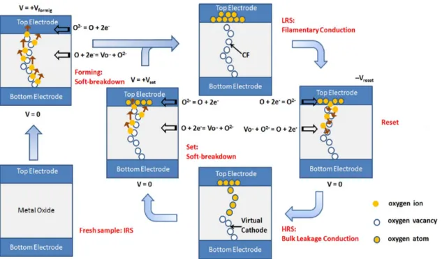
The oxygen vacancies are first created by the forming operation which has the role to redistribute them inside the insulating layer. These vacancies are positively charged and their migration is possible thanks to electric field stimulus. Through their removal and placing inside the insulating layer in the RESET and SET operation respectively, the memory behavior is possible. The process of creating the CF is very similar to the oxides breakdown, but given its reversibility, is commonly known as a Soft Breakdown [70].
Figure 1.10, presents a summary of the main steps undergoing on a typical bipolar OxRAM. In the same way as for CBRAM devices, a high current density for the RESET process accelerates the thermal heating of the filament and its consequent destruction [71].
Figure 1.9: SET and RESET for CBRAM devices. Switch is based on electrochemi-cal processes where metallic cations form non-volatile but erasable conductive filaments. Schematics shows a Ag TE and a Pt BE. Source: [57]
Hybrid devices
Hybrid ReRAM are CBRAM based memories where oxygen vacancies VO are introduced
inside the electrolyte to improve performances. In this type of memories, VO can improve
the percolation of the metallic ions inside the oxide reducing the switching voltages. A typical hybrid stack consists of a Cu TE with a HfO2insulating layer. Pristine resistances
can be reduced, but this implies that the memory window (difference between the LRS and HRS median values) is reduced too. On the other hand, endurance can be improved [72–74].
1.3.5.b Conduction models and working mechanisms of ReRAM technologies
To understand the physical processes taking place in resistive memories, it is necessary to categorize them into the most relevant ones. These are, the conduction mechanisms in the HRS and the LRS as well as the kinetics of the switching phenomena. Such characteristics have been the traditional development axes to propose a diversity of ReRAM models. This
Figure 1.10: Schematic process of the switching mechanism in oxide-based RAM (OxRAM) devices. Taken from: [70]
section summarizes some of them, where evidently, the working mechanisms of OxRAM and CBRAM memories are included.
Resistive memories are based on the switching properties of dielectric films, which present specific interactions (physical processes) under electrical stimulus, with the elec-trodes surrounding them, in order to have non-volatile and reversible states. Such di-electric materials present insulator characteristics, with a large band gap (> 3 eV ) and low electrical conductivity [75]. The conduction current of dielectric films when normal electric field is applied is very low. However, under high electric fields, current begins to increase, thanks to diverse conduction mechanisms. Under this scenario, it can be affirmed that dielectric materials are an extreme case of semiconductors [75].
To study the conduction current going through the dielectric film, the considered structure is extremely important. In the case of resistive memories, a MIM structure (Metal Insulator Metal) is the analyzed case. Since different materials are used for the top and bottom electrodes, asymmetry among the metal-dielectric interface barriers appears. This leads to different work functions and therefore, different bending between materials in order to satisfy the thermodynamic equilibrium. Band bending in turn, affects the quantum mechanical barrier shape [75].
Electronic conduction mechanisms
Resistive Memories applications can be either ionic, electronic or mixed ionic-electronic (Hybrid devices) materials [76]. Electrical conductivity changes with the states of the
resistive memory and as a function of the conduction mechanisms taking place inside the dielectric layer. They are classified between electron-limited and transport-limited or bulk-limited. For the former, the dielectric-electrode interface determines the conduction mechanisms as for the latter, they depend on the dielectric properties itself. Regard-less of the resistive state, various phenomena are always present in a simultaneous way with a different balance. Such balance changes when switching occurs, depending on the electric field, voltage polarity or the temperature. However, most of the time, a dominant mechanism is present, but with switching and current densities changing, such dominant mechanism changes too. A diagram of the conduction processes is presented in Figure 1.11, while an illustration of them can be found in Figure 1.12 [75, 76]
• Electron-limited conduction mechanisms. As mentioned before, these kind of conduction mechanisms depend on the electrode-dielectric barrier where the most important parameter is the barrier height at such interface. Another relevant factor is the effective mass of the conduction carriers. These type of mechanisms include Schottky or thermionic emission, Fowler-Nordheim tunneling, direct tunneling and tunneling from cathode to the dielectric traps (1). While current due to direct
tunneling is temperature independent, that one produced by Schottky emission is very dependent on the temperature.
• Bulk-limited conduction mechanisms. In this case, the behavior is determined by the trap energy level of the oxide, traps spacing and density, dift mobility, density of states in the conduction band, and the dielectric relaxation time. For the bulk-limited conduction mechanisms, emission from trap to the conduction band, Poole-Frenkel emission, which is a type of Fowler-Nordheim tunneling; trap to trap hopping and tunneling from traps to anode; are included [75].
As mentioned before, for CBRAM devices, ion hopping is the dominant conduction mechanism and it is determined by the Mott-Gurney equations [61]. A characteristic field E0, determines the behavior of the ionic current, which can be electric field or temperature
dependent [76].
In the case of OxRAM devices, several tunneling mechanisms take place. When the device is a perfect insulator (pristine state) and there is no presence of electrically active defects, conduction is governed by the direct tunneling. Once such defects are generated, through electric field application, further band bending appears and electron transmission is increased, leading to current increase. Moreover, if the barrier shape is degenerated to a triangular shape, a Fowler-Nordheim conduction regime appears. This in the case of non ultra-thin oxides (>2nm), where direct tunneling will be still dominant [75]. A transition can make an electron to surpass the energy barrier enhanced by temperature. In that case, a Schottky emission occurs.
(1)A trap is a location inside a semiconductor or insulator that restricts the movement of electrons or
holes. It can be a chemical impurity or an imperfection in the regular spacing of the atoms that make up the solid [77]
Figure 1.11: Types of conduction mechanisms taking place inside dielectric films which include ReRAM memories. Adapted from: [75]
Figure 1.12: Possible conduction mechanisms taking place inside resistive memories. Adapted from: [78]
Another mechanism used to explain conduction in OxRAM devices is the Poole-Frenkel regime [79–81]. There, an electron is excited into the conduction band through a trap site. This is originated by the presence of charged defects which lower the effective barrier height seen by electrons around a specific trap [75]. This conduction regime will be used in further chapters to estimate OxRAM currents in the OFF state.
Switching process and characteristics
Understanding the switching process is essential in order to improve resistive memories reliability, to control, and to predict device scaling. Due to insufficient stability and non-efficient energy consumption of unipolar devices, bipolar ones have gained considerable attention [82]. This is the reason why, the switching explanations presented in this sec-tion are mainly focused on bipolar ReRAM. All these characteristics are most known as switching kinetics and normally two aspects are limiting for the switching processes: ionic transport (where the Mott-Gurney equations are an example) and electron transfer reaction, which occurs at the electrode-insulator interface. These two mechanisms are temperature and electric field enhanced [76].
One of the additional factors that can be rate-limiting are phase transformations. They can be induced by local redox reaction and ion depletion. Its velocity is depending on an activation energy and can be temperature dependent. These are some of the reasons of the switching non-linearity once local Joule heating appears.
Concerning the switching characteristics, voltages required to effectuate either RESET or SET processes are dependent on the precedent programming state. As for the switching currents, their equivalence ISET ∼ IRESET has been validated thanks to experiments as
depicted in Figure 1.13(a) This empirical relation is explained by the non-linearity of the switching events, the I-V behavior of the LRS, and the weak dependence on materials properties, such as activation energies and diffusivity of the RESET switching voltage [83–85].
In the case of the SET operation, the conductive filament (CF) geometry and the chemical composition of the depleted gap, lead to a correlation between the initial state R and VSET [85]. On the other hand, various set resistances can be obtained as a function
of the SET current (See Figure 1.13(b).
Moreover, switching values present a strong dependence on the applied pulses too. Diverse HRS and LRS states can be obtained modifying the pulse characteristics or the compliance current. Every switch is related to a pulse width and amplitude. For example, increasing the pulse amplitude, will require a shorter time to make the device to switch [76].
1.4 SCM: a new memory market
As presented in precedent sections, emerging memory technologies open the door to im-prove the general performances of computing systems through the so-called Storage Class Memory applications; which could mix the high performances and robustness with the low cost and storage capacities of flash memories and hard-disk drives, respectively [86]. To this end, some techniques have been historically proposed and explored. Among them, 3D integration, high parallelism of multiple memory layers, and several bits stored per cell (mostly known as multi-levels per cell MLC), can be found [16].
Figure 1.13: (a).Empirical demonstration of the equivalence between RESET (maximum current before switch into the OFF state) and SET current (compliance IC). Various
materials are compared (b). Set and reset resistances as a function of IC. Compliance
current determines the CF cross section, IRESET and LRS/HRS values. Taken from: [85]
SCM are usually classified into two subcategories, as a function of the latency time and the storage capacity inside the memory gap between DRAM and Flash technologies: • Memory-type SCM [16] The M-type SCM are latency closer to DRAM memories. They would add lower power/GB, good retention to DRAM systems, and could be used to provide full recovery from crashes or power outages. Due to its proximity to DRAM memories, high cycling endurance is required.
• Storage-type SCM [16] The S-type SCM applications main objective is to have similar densities to those of flash technologies, but with a much faster access time, new direct overwrite and random access capabilities. This could allow simpler and more energy efficient systems. As for the other performances such as retention, it needs to be at least equivalent.
Some of the most important requirements for both of the subcategories of SCM ap-plications are summarized in Table 1.1. Through very specific requirements and direct comparisons with existing technologies, some conclusions can be inferred in order to know which emerging technologies are more adapted for specific applications. These targets, are defined in order to make of M-type and S-type real competitors and real innovations that could fill the memory gap and solve in someway, the memory bottleneck.


![Figure 2.13: Retention curve with failure time extraction at 130°C. Taken from: [1]](https://thumb-eu.123doks.com/thumbv2/123doknet/12870331.369249/87.892.231.657.219.555/figure-retention-curve-failure-time-extraction-c-taken.webp)

