HAL Id: hal-01139850
https://hal.archives-ouvertes.fr/hal-01139850
Submitted on 7 Apr 2015
HAL is a multi-disciplinary open access
archive for the deposit and dissemination of
sci-entific research documents, whether they are
pub-lished or not. The documents may come from
teaching and research institutions in France or
abroad, or from public or private research centers.
L’archive ouverte pluridisciplinaire HAL, est
destinée au dépôt et à la diffusion de documents
scientifiques de niveau recherche, publiés ou non,
émanant des établissements d’enseignement et de
recherche français ou étrangers, des laboratoires
publics ou privés.
SiOx /SiNy multilayers for photovoltaic and photonic
applications
Ramesh Pratibha Nalini, Larysa Khomenkova, Olivier Debieu, Julien Cardin,
Christian Dufour, Marzia Carrada, Fabrice Gourbilleau
To cite this version:
Ramesh Pratibha Nalini, Larysa Khomenkova, Olivier Debieu, Julien Cardin, Christian Dufour, et
al.. SiOx /SiNy multilayers for photovoltaic and photonic applications. Nanoscale Research Letters,
SpringerOpen, 2012, 7 (1), pp.1-6. �10.1186/1556-276X-7-124�. �hal-01139850�
N A N O E X P R E S S
Open Access
SiO
x
/SiN
y
multilayers for photovoltaic and
photonic applications
Ramesh Pratibha Nalini
1*, Larysa Khomenkova
1, Olivier Debieu
1, Julien Cardin
1, Christian Dufour
1, Marzia Carrada
2and Fabrice Gourbilleau
1Abstract
Microstructural, electrical, and optical properties of undoped and Nd3+-doped SiOx/SiNy multilayers fabricated by
reactive radio frequency magnetron co-sputtering have been investigated with regard to thermal treatment. This letter demonstrates the advantages of using SiNyas the alternating sublayer instead of SiO2. A high density of
silicon nanoclusters of the order 1019nc/cm3is achieved in the SiOxsublayers. Enhanced conductivity, emission,
and absorption are attained at low thermal budget, which are promising for photovoltaic applications. Furthermore, the enhancement of Nd3+emission in these multilayers in comparison with the SiOx/SiO2
counterparts offers promising future photonic applications.
PACS: 88.40.fh (Advanced materials development), 81.15.cd (Deposition by sputtering), 78.67.bf (Nanocrystals, nanoparticles, and nanoclusters).
Keywords: SiOx/SiNy, multilayers, Nd 3+
doping, photoluminescence, XRD, absorption coefficient, conductivity
Introduction
Silicon nanoclusters [Si-ncs] with engineered band gap [1] have attracted the photonic and the photovoltaic industries as potential light sources, optical interconnec-tors, and efficient light absorbers [2-5]. Multilayers [MLs] of silicon-rich silicon oxide [SiOx] alternated with SiO2 became increasingly popular due to the precise
control on the density and size distribution of Si-ncs [6,7]. Moreover, the efficiency of light emission from SiOx-based MLs exceeds that of the single SiOx layers with equivalent thickness due to the narrower Si-nc size distribution. The ML approach is also a powerful tool to investigate and control the emission of rare-earth [RE] dopants, for example, Er-doped SiOx/SiO2 MLs [8]. It
also allows us to control the excitation mechanism of the RE ions by adjusting the optimal interaction distance between the Si-ncs and the RE ions. However, achieving electroluminescence and hence extending its usage for photovoltaic applications are problematic due to the high resistivity caused by SiO2 barrier layers [9]. Hence,
replacement of the SiO2 sublayer by alternative
dielectrics becomes interesting. Due to the lower poten-tial barrier and better electrical transport properties of silicon nitride [Si3N4] in comparison to SiO2, multilayers
like SiOx/Si3N4 [10], Si-rich Si3N4(SiNy)/Si3N4 [11], and
Si-rich Si3N4/SiO2 [12] were proposed and investigated
[13] for their optical and electrical properties.
In this letter, we investigate SiOx/SiNyMLs and com-pare them with the SiOx/SiO2 counterparts reported
earlier [9,14]. We demonstrate that an enhancement in the conductive and light-emitting properties of SiOx/ SiNyMLs can be achieved with a reduced thermal bud-get. We also report a pioneering study on Nd-doped SiOx/SiNyMLs. A comparison between the properties of Nd3+-doped SiOx/SiO2 and SiOx/SiNy MLs are
pre-sented, and we show the benefits of using SiNysublayers
to achieve enhanced emission from Nd3+ions.
Experimental details
Undoped and Nd-doped 3.5-nm SiOx/5-nm SiNy(50
periods) MLs were deposited at 500°C on a 2-inch p-Si substrate by radio frequency [RF] magnetron co-sputter-ing of Si and SiO2 targets in hydrogen-rich plasma for
the SiOxsublayers and a pure Si target in nitrogen-rich plasma for the SiNysublayers. An additional Nd2O3
tar-get was used to dope the SiOx and SiNy sublayers by
* Correspondence: [email protected]
1
CIMAP UMR CNRS/CEA/ENSICAEN/UCBN, 6 Bd. Maréchal Juin, 14050 Caen Cedex 4, France
Full list of author information is available at the end of the article
© 2012 Nalini et al; licensee Springer. This is an Open Access article distributed under the terms of the Creative Commons Attribution License (http://creativecommons.org/licenses/by/2.0), which permits unrestricted use, distribution, and reproduction in any medium, provided the original work is properly cited.
Nd3+ions. More details on the growth process can be found elsewhere [15]. The excess Si content in the cor-responding SiOx and SiNy single layers obtained from
RBS studies are calculated to be 25 and 11 at.%, respec-tively (i.e., SiOx = 1and SiNy = 1.03). Conventional
fur-nace annealing under nitrogen atmosphere at different temperatures, TA= 400 to 1,100°C, and times,tA= 1 to
60 min, was performed on the MLs. X-ray diffraction analysis was performed using a Phillips XPERT HPD Pro device (PANalytical, Almelo, The Netherlands) with CuKaradiation (l = 0.1514 nm) at a fixed grazing angle incidence of 0.5°. Asymmetric grazing geometry was chosen to increase the volume of material interacting with the X-ray beam and to eliminate the contribution of the Si substrate. Photoluminescence [PL] spectra were recorded in the 550- to 1,150-nm spectral range using the Triax 180 Jobin Yvon monochromator (HOR-IBA Jobin Yvon SAS, Longjumeau, Paris, France) with an R5108 Hamamatsu PM tube (Hamamatsu, Shizuoka, Japan). The 488-nm Ar+laser line served as the excita-tion source. All the PL spectra were corrected by the spectral response of the experimental setup. Top and rear-side gold contacts were deposited on the MLs by sputtering for electrical characterization. Current-voltage measurements were carried out using a SUSS Microtec EP4 two-probe apparatus (SUSS Microtec, Germany) equipped with Keithley devices (Keithly, Cleveland, OH, USA). Energy-filtered transmission electron microscopy [EFTEM] was carried out on a cross-sectional specimen using a TEM-FEG microscope Tecnai F20ST (FEI, Eind-hoven, The Netherlands) equipped with an energy filter TRIDIEM from Gatan (Gatan, München, Germany). The EFTEM images were obtained by inserting an energy-selecting slit in the energy-dispersive plane of the filter at the Si (17 eV) and at the SiO2 (23 eV)
plas-mon energy, with a width of ± 2 eV.
Results and discussions
Effect of annealing on the PL
Since an annealing atTA= 1,100°C andtA= 60 min is
the most suitable to achieve an efficient PL from Si-ncs either in sputtered SiOx single layers [7] or in SiOx /SiO2 MLs [16], such treatment was first employed on
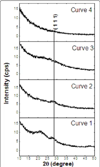
SiOx/SiNyMLs. The X-ray diffraction [XRD] broad peak
centered around 2θ = 28° is the signature of the Si nanoclusters’ formation in the SiOx /SiO2 (Figure 1,
curve 1) and SiOx/SiNy MLs (Figure 1, curve 2) as
already observed by means of atomic scale studies on similar multilayers [17]. However, contrary to the PL emission obtained from the SiOx/SiO2 MLs, no PL
emission was observed in the SiOx/SiNyMLs after such annealing (Figure 2a). This stimulated a deeper investi-gation of the post-fabrication processing to achieve effi-cient light emission from the SiOx/SiNyMLs.
It was observed that the PL signals from the MLs annealed during tA = 60 min are significant only at
lower temperatures (TA = 400°C to 700°C), and high
intensities are obtained when the samples are annealed at high temperatures for a short time (TA= 900°C to
1,000°C, tA = 1 min). It is interesting to note that an
interplay between TAand tAcan yield similar PL
effi-ciencies, as can be seen for TA= 900°C andtA= 1 min,
andTA= 700°C andtA= 15 min (Figure 2a).
The highest PL intensity in SiOx/SiNy MLs was obtained with TA= 1,000°C and tA= 1 min (Figure 2b,
c), whereas the SiOx/SiO2 MLs showed no emission
after such short-time annealing treatment (Figure 2a). Corresponding XRD pattern of this short-time annealed [STA] (STA = 1 min, 1,000°C) SiOx/SiNy showed a
broad peak in the range 2θ = 20° to 30° which is absent
Figure 1 XRD spectra of annealed Si-based MLs. (curve 1) SiOx/
SiO21 h, 1,100°C; (curve 2) SiOx/SiNy1 h, 1,100°C; (curve 3) SiOx/SiNy
1 min, 1,000°C; and (curve 4) SiOx/SiO21 min, 1,000°C.
Naliniet al. Nanoscale Research Letters 2012, 7:124 http://www.nanoscalereslett.com/content/7/1/124
in STA SiOx/SiO2 MLs (Figure 1, curves 3 and 4). This
suggests the presence of small Si clusters in the SiOx/ SiNyMLs, with lower sizes (broader peak) by compari-son with higher annealing temperature (1,100°C; Figure 1, curves 1 and 2). However, we cannot distinguish which of the sublayer is at the origin of the PL emission. Consequently, the recorded PL may be a combined con-tribution of the Si-ncs in the SiOx sublayers and the
localized bandtail defect states in the SiNysublayers. Absorption and electrical studies
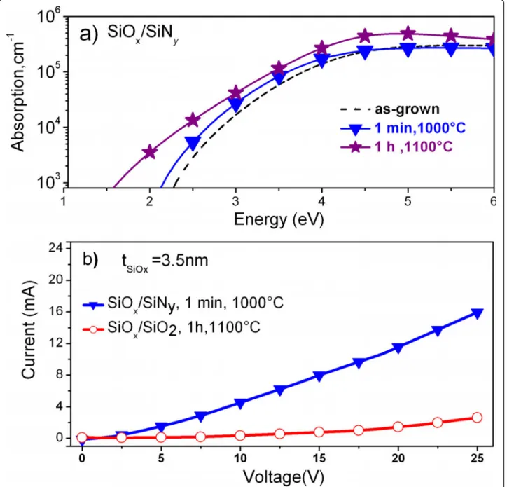
The absorption studies show similar absorption coeffi-cients for as-grown and STA MLs, whereas annealing at TA= 1,100°C andtA= 60 min results in an absorption
enhancement (Figure 3a). One can say that, at such temperature, an increase in density and size of the Si-ncs occurs due to phase separation of the SiOxsublayers into Si and SiO2 phases. The formation of Si
nanocrys-tals is complete at TA= 1,100°C and tA = 60 min and
leads to this enhancement. This reasoning is supported by the results obtained from the PL and the XRD analy-sis of the samples annealed at such temperature. The PL in the SiOx/SiNy MLs is quenched after an increase in
the time and temperatures of annealing (Figure 2a), and this can be attributed to the increase in the size leading to the loss of quantum confinement effect. The
formation of Si nanoclusters can be witnessed from the appearance of the XRD peak at 2θ = 28° (Figure 1, curve 2), which is not seen in the short-time annealed sample (Figure 1, curve 3).
Considering a balance between light emission and absorption for photovoltaic applications, we chose to study STA SiOx/SiNy MLs with a total thickness of 850
nm for electrical measurements. Figure 3b compares the dark current curves of 3.5-nm SiOx/5-nm SiNywith our
earlier reported 3.5-nm SiOx/3.5-nm SiO2 (140 nm)
MLs [14]. The resistivity was calculated at 7.5 V to be 2.15 and 214 MΩ·cm in the SiOx/SiNyand SiOx/SiO2
MLs, respectively. Since the thickness of the SiOx sub-layer is the same in both cases (3.5 nm), this decrease in the resistivity of the SiOx/SiNyMLs can be ascribed to
the substitution of 3.5-nm SiO2 by 5-nm SiNysublayers.
This hundred-times enhanced conductivity at low vol-tage paves way for further improvement of the SiOx/ SiNyMLs’ conductivity, for example, by decreasing the thickness of this SiNysublayer.
Microstructural studies
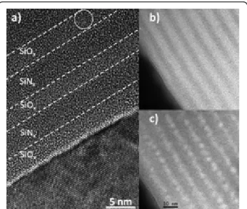
The high-resolution transmission electron microscope [HRTEM] and EFTEM observations on STA SiOx/SiNy
show Si-ncs in the SiOx sublayers with an average
dia-meter of 3.4 nm. Only a couple of Si nanocrystals were
Figure 2 Photoluminescence. (a) Maximum PL intensity [IPL] of SiOx/SiNyMLs vs TAand tA, and SiOx/SiO2at 1,100°C; (b) PL spectra of STA SiOx/
observed in the HRTEM (Figure 4a), whereas a high density of Si-nanoclusters of about 1019 nc/cm3can be witnessed from the EFTEM images taken at the Si plas-mon energy (Figure 4c) implying that they are predomi-nantly amorphous. Interestingly, this density of the Si-ncs in the SiOx/SiNy MLs is an order of magnitude higher than the Si-ncs formed in the SiOx/SiO2 MLs
fabricated under similar conditions. The brighter SiOx sublayers are distinguished from the darker SiNy
sub-layers by filtering the SiO2 plasmon energy (Figure 4b).
No evidence of Si-ncs within the SiNx sublayers was
obtained. The STA could favor the formation of Si-ncs only in SiOx and not in SiNysublayers. This could be attributed to the different mechanism of Si-ncs forma-tion in SiOxand SiNyin MLs as opposed to that in sin-gle layers [18] and/or the low Si-excess content in SiNy.
Effect of Nd3+-doping
Understanding the microstructure of MLs and consider-ing the enhancement of absorption and emission prop-erties in SiOx/SiNy MLs compared to the SiOx/SiO2
MLs, we investigate the effect of using SiNysublayer on
Figure 3 Absorption coefficient and current-voltage behavior. (a) Evolution of absorption coefficient with annealing; (b) Comparison of current-voltage behavior of SiOx/SiNyand SiOx/SiO2MLs.
Naliniet al. Nanoscale Research Letters 2012, 7:124 http://www.nanoscalereslett.com/content/7/1/124
the PL emission from Nd3+ions. For this purpose, the SiOx-Nd/SiNy-Nd and SiOx-Nd/SiO2-Nd MLs were
fab-ricated, and their PL properties were compared. No PL emission was detected from the Nd3+-doped SiNysingle
layers at the different annealing treatments investigated here. Figure 5 shows the PL spectra of the Nd3+-doped as-grown MLs under non-resonant excitation with peaks corresponding to the4F3/2® 4I 9/2 and 4F 3/2® 4I 11/2
tran-sitions at 1.37 and 1.17 eV, respectively. The comparison between the PL properties of undoped (Figure 2c) and Nd3+-doped MLs (Figure 5, inset) clearly shows the quenching of visible PL emission and the appearance of two Nd3+-related PL peaks in the Nd-doped MLs. More-over, the intensity of Nd3+PL from the doped SiOx/SiNy MLs exceeds that of the SiOx/SiO2 MLs (Figure 5,
inset). Thus, we deal with the efficient energy transfer towards Nd3+ ions not only in SiOx but also in SiNy
sublayers. Since this emission is observed for as-grown MLs, when no Si-ncs were formed in these MLS, it is obvious that the emission from the Nd3+ions in the SiNx-Nd sublayers is due to an efficient energy transfer
from SiNy-localized defect states towards the Nd3+ions
[19,20]. PL observed from the doped MLs after STA was not intense, and it was quenched with increasing annealing time. The same behavior was observed for the 900°C annealing. This could be due to the decrease in the number of defect-related sensitizers in SiNyand the formation of Nd2O3 clusters in the SiOxsublayers [21].
On the other hand, annealing at TA = 400°C to 700°C,
Figure 4 HRTEM (a) and EFTEM (b, c) images. SiOx/SiNyML
annealed at TA= 1,000°C, tA= 1 min by filtering the energy at SiO2
plasmon (b) and Si plasmon (c) energies, respectively.
Figure 5 PL intensity with annealing time and temperature. Evolution of the Nd3+PL intensity at 1.37 eV for doped SiOx/SiNyMLs with
annealing temperature and time. (Inset) PL spectra of as-grown Nd3+-doped SiO
x/SiNyand SiOx/SiO2MLs with equal number of periods. The
discussed above for the undoped SiOx/SiNy MLs,
enhance Nd3+ PL emission when applied to the doped counterparts (Figure 3). Thus, we attain intense PL at a low thermal budget withTA(400°C to 700°C) and tA(1
min). To optimize Nd3+ emission, the effect of the thickness of each sublayer in SiOx/SiNy MLs is under consideration now.
Conclusion
In conclusion, we show that SiOx/SiNyMLs fabricated by RF magnetron sputtering can be engineered as struc-tures for photovoltaic and photonic applications. The as-grown and STA SiOx/SiNyMLs show enhanced
opti-cal and electriopti-cal properties than the SiOx/SiO2
counter-parts. Besides achieving a high density of Si-ncs at a reduced thermal budget, we show that high emission and absorption efficiencies can be achieved even from amorphous Si-ncs. The Nd-doped MLs, as-grown and those annealed at lower thermal budgets, demonstrate efficient emission from rare-earth ions. We also show that our STA SiOx/SiNy MLs have about a hundred times higher conductivity compared to the SiOx/SiO2
MLs. These results show the advantages of SiOx/SiNy MLs as materials for photovoltaic and photonic applica-tions and open up perspectives for a detailed study.
Abbreviations
MLs: multilayers; PL: photoluminescence; Si-nc: silicon nanoclusters; SiNy:
silicon-rich silicon nitride; SiOx: silicon-rich silicon oxide; STA: short time
annealing at 1,000°C for 1 min.
Acknowledgements
This study is supported by the DGA (Defense Procurement Agency) through the research program no. 2008.34.0031. The authors acknowledge J. Pierriére for the RBS measurements done with the SAFIR accelerator (INSP, UPMC) and X. Portier (CIMAP) for the TEM image.
Author details
1CIMAP UMR CNRS/CEA/ENSICAEN/UCBN, 6 Bd. Maréchal Juin, 14050 Caen
Cedex 4, France2CEMES/CNRS, 29 rue J. Marvig, 31055 Toulouse, France
Authors’ contributions
RPN fabricated the undoped multilayers under investigation and carried out the characterization studies. LK and OD fabricated the Nd-doped layers and studied the effect of Nd doping on the MLs. JC and CD made contributions to the optical studies. MC performed the EFTEM measurements. FG conceived of the study and participated in the coordination of the manuscript. All authors read and approved the final manuscript.
Competing interests
The authors declare that they have no competing interests.
Received: 11 October 2011 Accepted: 14 February 2012 Published: 14 February 2012
References
1. Canham LT: Silicon quantum wire array fabrication by electrochemical and chemical dissolution of wafers. Appl Phys Lett 1990, 57:1046. 2. Pavesi L, Dal Negro L, Mazzoleni C, Franzo G, Priolo F: Optical gain in
silicon nanocrystals. Nature 2000, 408:440.
3. Irrera A, Franzo G, Iacona F, Canino A, Di Stefano G, Sanfilippo D, Piana A, Fallica PG, Priolo F: Light emitting devices based on silicon
nanostructures. Physica E 2007, 38:181.
4. Garrido B, Lopez M, Pérez Rodriguez A, Garcia C, Pellegrino P, Ferré R, Moreno JA, Morante JR, Bonafas C, Carrada M, Claverie A, De La Torre J, Souifi A: Optical and electrical properties of silicon nanocrystals ion-beam synthesized in SiO2. Nucl Inst Meth Phys B 2004, 216:231.
5. Conibeer G, Green MA, Corkish R, Cho Y, Cho EC, Jiang CW, Fangsuwannarak T, Pink E, Huang Y, Puzzer T, Trupke T, Richards B, Shalav A, Lin KL: Silicon nanostructures for third generation photovoltaic solar cells. Thin Solid Films 2006, 511:654.
6. Zacharias M, Heitmann J, Scholz R, Kahler U, Schimdt M, Blasing J: Size controlled highly luminescent silicon nanocrystals: a SiO/SiO2
superlattice approach. Appl Phys Lett 2002, 80:661.
7. Gourbilleau F, Portier X, Ternon C, Voivenel V, Madelon R, Rizk R: Si-rich/ SiO2nanostructured multilayers by reactive magnetron sputtering. Appl
Phys Lett 2001, 78:3058.
8. Gourbilleau F, Dufour C, Madelon R, Rizk R: Effects of Si nanocluster size and carrier Er interaction distance on the efficiency of energy transfer. J Lumin 2007, 126:581.
9. Maestre D, Palais O, Barakel D, Pasquinelli M, Alfonso C, Gourbilleau F, De Laurentis M, Irace A: Structural and optoelectronical characterization of Si-SiO2/SiO2multilayers with applications in all Si tandem solar cells.
J Appl Phys 2010, 107:064321.
10. Di D, Perez-Wurfl I, Conibeer G, Green MA: Formation and
photoluminescence of Si quantum dots in SiO2/Si3N4hybrid matrix for
all-Si tandem solar cells. Solar Energy Materials & Solar Cells 2010, 94:2238. 11. So YH, Huang S, Conibeer G, Green MA: Formation and
photoluminescence of Si nanocrystals in controlled multilayer structure comprising of Si-rich nitride and ultrathin silicon nitride barrier layers. Thin Solid Films 2011, 519:5408.
12. Delachat F, Carrada M, Ferblantier G, Grob JJ, Slaoui A, Rinnert H: The structural and optical properties of SiO2/Si rich SiNxmultilayers
containing Si-ncs. Nanotechnology 2009, 20:275608.
13. Conibeer G, Green MA, Perez- Wurfl I, Huang S, Hao X, Di D, Shi L, Shrestha S, Puthen-Veetil B, So Y, Zhang B, Wan Z: Silicon quantum dot based solar cells: addressing the issues of doping, voltage and current transport. Prog Photovolt: Res Appl Paper presented at the 25th EU PVSEC WCPEC-5, Spain; 2010.
14. Pratibha Nalini R, Dufour C, Cardin J, Gourbilleau F: New Si-based multilayers for solar cell applications. Nanoscale Res Lett 2011, 6:156. 15. Ternon C, Gourbilleau F, Portier X, Voivenel P, Dufour C: An original
approach for the fabrication of Si/SiO2multilayers using reactive
magnetron sputtering. Thin Solid Films 2002, 419:5.
16. Gourbilleau F, Ternon C, Maestre D, Palais O, Dufour C: Silicon-rich SiO2/
SiO2multilayers: a promising material for the third generation of solar
cell. J Appl Phys 2009, 106:013501.
17. Talbot E, Lardé M, Gourbilleau F, Dufour C, Pareige P: Si nanoparticles in SiO2: an atomic scale observation for optimization of optical devices. EPL 2009, 87:26004.
18. Dal Negro L, Yi JH, Michel J, Kimerling MC, Chang TWF, Sukhovatkin V, Sargent EH: Light emission efficiency and dynamics in silicon-rich silicon nitride films. Appl Phys Lett 2006, 88:233109.
19. Biggemann D, Tessler LR: Near infra-red photoluminescence of Nd3+in
hydrogenated amorphous silicon sub-nitrides a-SiNx:H <Nd>. Mat Sci Eng B 2003, 105:188.
20. Lin R, Yerci S, Kucheyev SO, Van Buuren T, Dal Negro L: Energy transfer and stimulated emission dynamics at 1.1μm in Nd-doped SiNx.. Optics
Express 2011, 19:5379.
21. Debieu O, Bréard D, Podhorodecki A, Zatryb G, Misiewicz J, Labbé C, Cardin J, Gourbilleau F: Effect of annealing and Nd concentration on the photoluminescence of Nd3+ions coupled with silicon nanoparticles.
J Appl Phys 2010, 108:113114.
doi:10.1186/1556-276X-7-124
Cite this article as: Nalini et al.: SiOx/SiNymultilayers for photovoltaic
and photonic applications. Nanoscale Research Letters 2012 7:124.
Naliniet al. Nanoscale Research Letters 2012, 7:124 http://www.nanoscalereslett.com/content/7/1/124
![Figure 2 Photoluminescence. (a) Maximum PL intensity [I PL ] of SiO x /SiN y MLs vs T A and t A , and SiO x /SiO 2 at 1,100°C; (b) PL spectra of STA SiO x / SiN y MLs; (c) I PL vs T A for t A = 1 min](https://thumb-eu.123doks.com/thumbv2/123doknet/13752363.437826/4.892.87.806.135.564/figure-photoluminescence-maximum-intensity-sio-sin-mls-spectra.webp)