HAL Id: hal-02146131
https://hal.archives-ouvertes.fr/hal-02146131
Submitted on 12 Jun 2019HAL is a multi-disciplinary open access archive for the deposit and dissemination of sci-entific research documents, whether they are pub-lished or not. The documents may come from teaching and research institutions in France or abroad, or from public or private research centers.
L’archive ouverte pluridisciplinaire HAL, est destinée au dépôt et à la diffusion de documents scientifiques de niveau recherche, publiés ou non, émanant des établissements d’enseignement et de recherche français ou étrangers, des laboratoires publics ou privés.
Weak localization and electron-electron interactions in
polycrystalline tin dioxide films
V Ksenevich, Taras Dauzhenka, J. Galibert
To cite this version:
V Ksenevich, Taras Dauzhenka, J. Galibert. Weak localization and electron-electron interactions in polycrystalline tin dioxide films. 20th International Conference on the Application of High Magnetic Fields in Semiconductor Physics (HMF), Jul 2012, CHAMONIX, France. pp.012022, �10.1088/1742-6596/456/1/012022�. �hal-02146131�
Journal of Physics: Conference Series
OPEN ACCESS
Weak localization and electron-electron
interactions in polycrystalline tin dioxide films
To cite this article: V K Ksenevich et al 2013 J. Phys.: Conf. Ser. 456 012022
View the article online for updates and enhancements.
Related content
Magnetoresistance in a High Mobility Two-Dimensional Electron System as a Function of Sample Geometry
L Bockhorn, A Hodaei, D Schuh et al.
-Quantum Hall effect in monolayer, bilayer and trilayer graphene
C Cobaleda, E Diez, M Amado et al.
-Effects of Rashba spin splitting and exchange interaction in electron spin resonance in narrow-gap quantum well heterostructures
S S Krishtopenko, K V Maremyanin, A V Malyzhenkov et al.
Weak localization and electron-electron interactions in
polycrystalline tin dioxide films
V K Ksenevich1, T A Dauzhenka1 and J Galibert2
1
Department of Physics, Belarusian State University, Nezalezhnastsi Ave. 4, 220030, Minsk, Belarus
2
Laboratoire National des Champs Magnétiques Intenses CNRS, Université de Toulouse, UPS, INSA Toulouse, UJF, 143 Avenue de Rangueil F-31400 Toulouse, France
e-mail address: [email protected]
Abstract. Electrical and magnetotransport properties of polycrystalline tin dioxide films were
investigated in the temperature range 2-300 K and in high magnetic fields up to 27 T. The experimental data were analyzed using models inherent both for 2D and 3D disordered systems. A crossover from 2D to 3D behaviour was observed as the temperature was increased.
1. Introduction
Besides a number of perspective applications in optoelectronics due to the coexistence of high optical transparency in visible and infrared range of electromagnetic waves’ spectra and high electrical conductivity [1], tin dioxide films provide the possibility to study different charge transport mechanisms, such as hopping, tunneling, diffusion transport. Quantum corrections to conductivity in the vicinity of metal-insulator transition as a result of weak localization (WL) and electron-electron interactions (EEI) phenomena can be also observed in tin dioxide films [2].
We recently reported the observation of negative magnetoresistance (MR) due to WL and EEI in thin polycrystalline tin dioxide films fabricated by means of combination of ion-exchange processes in polymer films with successive gas transport reaction [3].
In this work we focus our efforts on investigations of WL and EEI in polycrystalline tin dioxide (obtained from SnCl2 solution) by means of MR measurements in high magnetic fields. Temperature dependencies of the resistance R(T) and MR of polycrystalline tin dioxide films were measured within temperature range 2-300 K and in pulsed magnetic fields up to 27 T. The experimental data were analysed using models inherent both for 2D and 3D disordered systems [4]. A crossover from 2D to 3D behaviour was observed as the temperature was increased.
2. Fabrication of samples
The samples of SnO2 polycrystalline films were fabricated following a three-stage procedure [5]: (a) formation (on either Al2O3 or Si/SiO2 substrates) of a Sn-containing polymer networks, (b) gas transport of tin chloride vapour [as a result of the heating of the tin chloride hydrate (SnCl2. 2H2O)] on the substrates with previously deposited Sn-containing networks. After the deposition of tin chloride on the substrate, it was decomposed to the tin (II) oxide during the thermohydrolysis, (c) during the
HMF-20 IOP Publishing
Journal of Physics: Conference Series 456 (2013) 012022 doi:10.1088/1742-6596/456/1/012022
Content from this work may be used under the terms of theCreative Commons Attribution 3.0 licence. Any further distribution of this work must maintain attribution to the author(s) and the title of the work, journal citation and DOI.
subsequent heat treatment in air at temperature 550 oC, SnO was transformed to SnO2. Electron diffraction results confirmed the polycrystallinity (type cassiterite) of obtained films. Typical SEM image of tin dioxide film is shown in figure 1.
Figure 1. SEM image of tin dioxide films (after gas-transport reaction). 3. Experimental results and discussion
3.1. Temperature dependence
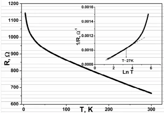
Typical R(T) dependence for SnO2 film is presented in figure 2.
Figure 2. Temperature dependence of resistance of SnO2 film. In the inset figure temperature dependence of conductance in the scale 1/R-Ln T is shown. Dashed line corresponds to linear
approximation of experimental data at low T.
HMF-20 IOP Publishing
Journal of Physics: Conference Series 456 (2013) 012022 doi:10.1088/1742-6596/456/1/012022
Such types of R(T) dependencies (with negative temperature coefficient of the resistance (dR/dT<0) and ratio R(2 K)/R(300 K)~1-2) are inherent for different disordered systems in the vicinity of metal-insulator transition. WL and EEI effects define the temperature dependence of conductivity of these systems [4].
Figure 3. Temperature dependence of resistance of SnO2 film in the scale 1/R- T1/2 is shown. Dashed line corresponds to linear approximation of experimental data in the intermediate temperature range. At low temperatures temperature dependence of conductivity for 2D disordered systems can be expressed as [6]: h τ + + σ = σ K G kT T T aG ee D ln 0ln 0 0 0 2 , (1)
where first term is a constant related to the residual conductivity of the system at T=0 K, the second and the third term are the temperature dependence of conductivity due to effects WL and EEI, respectively. Thus, according Eq. (1) both the WL and EEI produce ~lnT dependence of conductivity of 2D disordered systems.
Temperature dependence of conductivity for 3D disordered systems follows the law[7]: 2 / 2 / 1 0 3 p D =σ +αT +βT σ , (2)
taking into account both WL and EEI effects. The first term is a constant related to the residual conductivity of the system at T=0 K, the second and the third terms takes into account the effects of EEI and WL, respectively. If the characteristic length parameters, describing WL and EEI (inelastic scattering length Lφ=(Dτφ)1/2 and thermal length LT=(Dћ/kBT) , respectively, where D being the
diffusion constant, τ
B
1/2
φ is the inelastic scattering time), exceeds the thickness of the system, the
temperature dependence of the resistance follows a behaviour inherent for 2D disordered systems. As far as Lφ and LT are temperature dependent parameters, which decrease when the temperature rises, a
crossover from the σ(T) behaviour typical for 2D systems to the behaviour inherent for 3D disordered materials is expected as the temperature increases. As one can see from inset to Fig.2, ~lnT
HMF-20 IOP Publishing
Journal of Physics: Conference Series 456 (2013) 012022 doi:10.1088/1742-6596/456/1/012022
dependence of conductivity is observed in the low temperature range (up to ~27 K). In the temperature range T ~ 27-105 K dependence of conductivity on temperature can be linearized in scale σ – T as shown in Fig.3. Thus, we can assume existence of crossover from 2D to 3D behaviour for SnO
1/2
2 films at T ~ 27K with prevailing of quantum corrections to conductivity due to EEI.
3.2. Magnetic field dependences
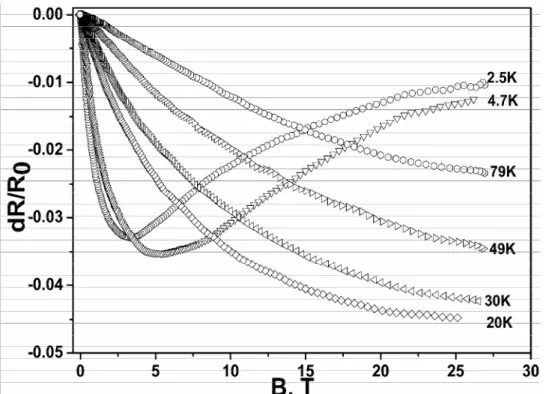
MR data measured in pulsed magnetic fields up to 27 T and in the temperature range 2.5-80 K are shown in Fig.4. The negative MR in the whole range of available magnetic fields was observed. In the low-temperature range upturn from negative to positive MR with tendency to saturation in the high magnetic field range was observed. The minimum position of negative MR shifts to higher fields as the temperature rises. At temperatures T>15 K only negative MR was observed.
Figure 4. Magnetic field dependences of normalized magnetoresistance of SnO2 films obtained from SnCl2 solution, measured in the temperature range 2.5-80 K.
Negative MR due to WL effect usually dominates at higher temperatures and lower fields, while at lower temperatures and higher fields, such
that the energy difference between the Zeeman split
levels is much more than the thermal energy (gμ
BH>>kB BBT) electron-electron interactions
should be taken into account,
providing possibility to observe positive MR.Existence of both negative and positive MR indicate on the possibility of interplay of EEI in addition to WL effects in polycrystalline tin dioxide films. Detailed analysis of MR data in order to distinguish influence of WL and EEI by means of method proposed in [8] will be reported elsewhere. 4. Conclusion
Quantum corrections to conductivity of thin polycrystalline tin dioxide films, fabricated by means of combination of ion-exchange processes in polymer films with successive gas transport reaction, were observed. Both weak localization (WL) and electron-electron interactions (EEI) effects can influence on the conductivity of films. A crossover from 2D to 3D behaviour was observed at temperature T~ 27 K.
HMF-20 IOP Publishing
Journal of Physics: Conference Series 456 (2013) 012022 doi:10.1088/1742-6596/456/1/012022
Acknowledgments
We acknowledge support from by FR7 I3 EuroMagnet II and by CNRS/BRFFI grant No. F11F-007. The authors are grateful to I.A. Bashmakov for samples’ fabrication, P.I. Gaiduk and S.V. Gusakova for implementation of TEM and SEM measurements.
One of us (T.D.) acknowledges the Embassy of France in Minsk for a French Foreign Affairs Ministry PhD grant.
References
[1] Batzill M and Diebold U 2005 Progress in Surface Science 79 47 [2] Serin T et al 2010 J. Electron. Mater. 39 1152
[3] Dauzhenka T A et al 2011 Phys. Rev. B 83 165309
[4] Lee P A and Ramakrishnan T V 1985 Rev. Mod. Phys. 57 287
[5] Bashmakov I A, Dauzhenka T A and Ksenevich V K 2009 Proceedings of IV International
Conference: Actual Problems of Solid State Physics ( Minsk) [in russian] 2 43
[6] Minkov G M et al 2001 Phys. Rev. B 64 235327
[7] Dai P, Zhangand Y and Sarachik M P 1992 Phys. Rev. B. 45 3984 [8] Bogdanovich S et al 1995 Phys. Rev. Lett. 74 2543
HMF-20 IOP Publishing
Journal of Physics: Conference Series 456 (2013) 012022 doi:10.1088/1742-6596/456/1/012022