Characterization of Nanostructured Hexagonal
Boron Nitride Patterned via
High-Resolution Ion Beam Lithography
by
Josu6 Jacob Lopez
B.S., Rice University (2014)
JUN 23 2017
LIBRARIES
Submitted to the Department of Electrical Engineering and Computer
Science
in partial fulfillment of the requirements for the degree of
Master of Science
at the
MASSACHUSETTS INSTITUTE OF TECHNOLOGY
June 2017
@
Massachusetts Institute of Technology 2017. All rights reserved.
Author
....
Certified by
Signature redacted
DeparTet of Et
cal Engineering and Computer Science
- I
Signature redacted
Marin Solja'id
Professor of Physics
Thesis Supervisor
Accepted by....
Signature redacted...
)
1/
U
Leslie Kolodziejski
Chair, Department Committee on Graduate Theses
ARCHIVES
Characterization of Nanostructured Hexagonal Boron Nitride
Patterned via
High-Resolution Ion Beam Lithography
by
Josue Jacob Lopez
Submitted to the Department of Electrical Engineering and Computer Science on May 19, 2017, in partial fulfillment of the
requirements for the degree of Master of Science
Abstract
The forefront of polariton research in two-dimensional (2D) materials focuses on push-ing the limits of patternpush-ing 2D materials into nanoresonators and other nanophotonic structures that manipulate highly confined polaritons for technologically relevant near-IR and mid-IR applications. Furthermore, tuning the properties of hexago-nal boron nitride, graphene, and other 2D materials in-plane and stacking them into heterostructures has the potential to create hybrid optical, electronic, thermal, and mechanical properties with a wealth of new functions. To fully tailor these novel properties, controlled nanoscale patterning of these and other van der Waals ma-terials is essential. Moreover, it becomes imperative to understand how patterning and geometries modify the properties within each layer or introduce defects that affect the interfaces of layered 2D heterostructures. Herein, we demonstrate high-resolution patterning of h-BN via both helium and neon ion beams and pattern a
h-BN grating with a 35 nm pitch and 20 nm feature size. We study varying degrees
of nanostructuring and defects via Raman spectroscopy, photo-thermal microscopy, and scattering-type scanning near-field optical microscopy and observe complimentary information about the phonon modes and the absorption and scattering of light from such nanostructures. Specifically, we observe geometry and layer dependent photo-thermal expansion of h-BN nanostructures that are mediated by phonons. This work demonstrates a thorough understanding of directly patterned 2D materials with ion beams and demonstrates that far-field and near-field measurements are essential in understanding how the nanostructuring of 2D materials can tune their properties. Thesis Supervisor: Marin Soljaid6
Acknowledgments
An enormous thank you to my family for their support, love, and understanding as
I have been away from home for over seven years pursuing my career in science. I
don't know how my mother did it, but as my brother and I grew up, she worked part time, took care of the family, and after many years of shear determination obtained a bachelor's degree (all while struggling to master English as a second-language after immigrating to the U.S.). She did this to show us the value of education. To my father, who showed my brother and I the value of hard work, precision, and most important of all - integrity. He would have been an excellent engineer had he been offered the same opportunities my brother and I were fortunate to have. To my younger brother Ivan, you always wanted to do what I was doing in school (as I was two years ahead), and by the time you were in high school you were inspiring me with your interests in physics, computer science, and robotics. Your intelligence inspires and pushes me and your humor makes me enjoy life a bit more (in all honesty... a lot more).
To my Tia Any, my cousins, and all my extended family in Houston, Texas who took me in as one of their own sons. To Ms. Woods from Duncan College (Rice University) you were always looking out for me and spreading love.
To Jessica, you have been a fantastic partner over more than 5 years. I could not ask for a more understanding and loving partner. I'm looking forward to what the future has in store for us.
To my friends and teachers from Lynwood, CA who taught and pushed me to be diligent, not back down, and push farther regardless of our social or economic back-ground (and to always give back once we made it). I am proud to say many of my friends have become leaders in the community. We are making a difference. To my dear friends who I have met at UC Berkeley (Pilam), East Los Angeles College
(MESA), Rice University (The Physics "Bros" - highly diverse in our race, gender,
and backgrounds; and the Mellon Mays Undergraduate Fellowship Program - "once a Mellon, always a Mellon"), Northwestern University, Caltech, and now MIT (ACME, Fossil Free MIT, EECS, and Physics Dept.). There are too many individuals to name here, you have been my family away from home in this incredible journey.
ELAC Acknowledgments:
Sincere thanks goes to Prof. Armando M. Rivera-Figueroa, Marina Rueda, Karla Gonzalez, and all my teachers and mentors at ELAC who helped me reestablish my foundation after being academically dismissed from UC Berkeley. You gave me a second chance at my academic career. Without you this would not have been possible. Rice University Acknowledgments:
An eternal thank you to Prof. Richard Tapia. Without you I would not have fully believed in my dream of going to MIT (and in my dream/goal to pursue academia). Without your guidance and mentorship there was a possibility that I would have left physics during my sophomore year. Your brilliance, tenacity, and leadership have inspired me to meet the highest standards of "global excellence". And whenever I feel like I'm not the very best I always go back to two of your core messages: "You don't have to be the best, you just have to be good enough," and "If you sit on the porch with the big dogs, and occasionally bark like a big dog, the world will view you as a big dog."
Thanks to Jason, Doug, and the rest of the Physics Faculty and Department. Your support and guidance throughout my undergraduate career at Rice helped me navi-gate physics and research.
MIT Acknowledgments:
Thank you to Marin for your guidance and support during the past 3 years. You have given me the freedom to develop into my own researcher. Thanks to John (JJ),
Vladimir, Leslie, and Terry. I have the best set of MIT faculty advocates and mentors I could have asked for. Thank you to the Soljani6 Group for the continued inspiration. I'm fortunate that I still have 2-3 years with you as I move on to the next step and seek my PhD here at MIT. Thanks to the ONE Lab and all its members, you have been my second "group" at MIT.
There are many more people to thank, please forgive me if I did not include you. Regardless, I will make sure to always give my gratitude in person. Fortunately, I will have a second opportunity to do so in my PhD Thesis. This is just the beginning of many more things to come!
Contents
1 Introduction 15
1.1 Proposing a graphene-plasmon-based table-top X-ray source . . . . . 15
1.1.1 State of the art methods for creating X-ray radiation . . . . . 17
1.1.2 Leveraging graphene plasmons . . . . 18
1.1.3 Leveraging standard transmission electron microscopes . . . . 19
1.2 Introduction: Graphene plasmons . . . . 19
1.3 Introduction: Motivations for h-BN nanoscale gratings . . . . 21
2 Fabrication and characterization of h-BN gratings 25 2.0.1 Monte Carlo simulations . . . . 26
2.0.2 Characterization of h-BN grating . . . . 26
2.0.3 Atomic force microscopy . . . . 26
2.0.4 Raman spectroscopy . . . . 27
3 Scanning probe microscopy of h-BN gratings 35 3.0.5 Photo-thermal spectroscopy and imaging . . . . 35
3.0.6 Scattering-type scanning near-field optical microscopy . . . . . 38
4 Conclusion 43 A Methods 45 A.1 Sample preparation . . . . 45
A.3 Monte carlo simulations of ion beam
interactions . . . . 46
A.4 Atomic force microscopy . . . . 47
A.5 Raman spectroscopy . . . . 47
A.6 Photo-thermal spectroscopy and imaging . . . . 47
List of Figures
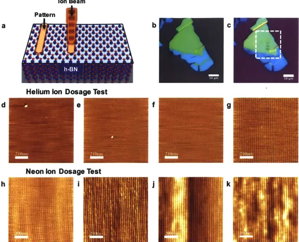
2-1 Hexagonal boron nitride nanopatterning. (a) Illustration of nano
patterning due to ion bombardment. (b, c) Optical micrograph before and after ion beam patterning. Helium versus neon ion dosage. Atomic force microscope scans of (d-g). The array of patterned lines goes from left to right. Each line is etched from top to bottom. The horizontal artifacts are AFM noise. Helium ion dosages at 30 keV.
(d) 1,000 pC/cm. (e) 10,000 pC/cm. (f) 20,000 pC/cm. (g) 40,000
pC/cm. Helium dosages between 20,000 and 40,000 pC/cm clearly defined the pattern. (h-k) Neon ion dosages at 25 keV. (h) 1,000 pC/cm. (i) 10,000 pC/cm. (j) 20,000 pC/cm. (k) 40,000 pC/cm. Neon
dosages between 1,000 and 40,000 pC/cm clearly defined the pattern. 30
2-2 Monte Carlo simulations of ion trajectories. Simulations compar-ing the range and trajectory of (a) 30 keV He ions in a 56.5 nm-thick
h-BN and (b) 25 keV Ne ions in a 45 nm-thick h-BN on top of the
SiO2/Si substrate. (c-d) Atomic distributions for each simulation
pro-vide the number of ions that undergo recoil at a specific ion dosage. The Ne ion causes over 10x more boron and nitrogen ions to undergo recoil. In collaboration with David C. Bell, Center for Nanoscale Sys-tems, Harvard University. . . . . 31
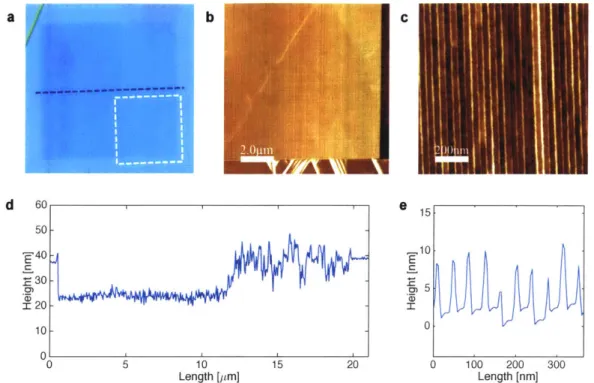
2-3 Hexagonal boron nitride grating with optimal neon dosage.
(a) Optical image of a 20 pm2
h-BN grating fabricated via neon ion
beam patterning at 25 keV. The difference in optical contrast is due to
a gradient in height. (b-c) AFM scans of the h-BN grating. (b) 10 1rM2
scan of bottom right corner in Fig. 2-3(a) denoted by the white dashed box. (c) High-resolution 1 rm2
scan of the milled pattern (using a 7 nm tip radius). (d) Cross-section of the entire grating which is represented
by the blue dashed line in Fig. 2-3(a). (e) Cross-section of the 1 prM2
scan confirming a pitch of 35 nm, a mill depth between 6-8 nm, and a nanostructure width of ~20 nm. . . . . 32
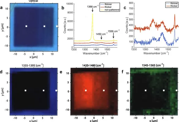
2-4 Raman spectroscopy and Raman maps. (a) Optical image of the h-BN grating. (b) Raman spectrum comparing locations inside and
outside the grating region. Plot includes h-BN phonon mode at 1366
cm-1, third order silicon TO phonon at 1450 cm-1, and ambient oxygen
at 1556 cm- 1. (c) Plot of Raman spectrum inside the thinner and thicker regions of the grating. (d-e) Raman maps showing the value of the integrated area under the peaks found within the ranges 1340-1390
cm- 1, 1425-1475 cm- 1, and 1540-1570 cm- 1. All maps are normalized
to the maximum counts found within each range. (d) Intensity map of the h-BN phonon peak at 1366 cm-1. (e) Intensity map of the silicon TO phonon at 1450 cm- 1. (f) Intensity map of peak at 1550 cm- 1 due to ambient oxygen. . . . . 33
3-1 Photo - thermal infrared spectroscopy and imaging. (a) Schematic
of photo-thermal illumination/detection system (b) AFM image with the location of all photo-thermal (absorption) spectrums taken. Num-bers correspond to locations of the plotted spectrums. (c) Photo-thermal spectrums taken from four different locations along the thicker region of the h-BN grating, strong and broad h-BN absorption peak at -1368 cm 1. (d) Photo-thermal spectrum taken from four differ-ent locations along the thinner region of the h-BN grating showing a strong SiO2 absorption peak at ~1084
cm-1. Photo-thermal Imaging
(e) AFM image of the top right corner of the h-BN grating indicated
by the white dashed box in Fig. 3-1(b). (f) Photo-thermal image of the
top right corner at 1368 cm- 1. (g) Photo-thermal image of the same region at 1600 cm . . . .
.
40
3-2 s - SNOM. (a) Topography scan taken of the entire grating structure. (b) s-SNOM image taken at 1368 cm- 1. (c) s-SNOM image taken at 1425 cm-1. (d) zoomed-in 3 pm2
topography scan, region highlighted
by the white box in Fig. 3-2(a). (e) 3 pm2 s-SNOM image taken at 1368
cm 1. (f) 3 pm2
s-SNOM image taken at 1425 cm-1. In collaboration with Siyuan Dai, Department of Physics, University of California, San
D iego. . . . . 41
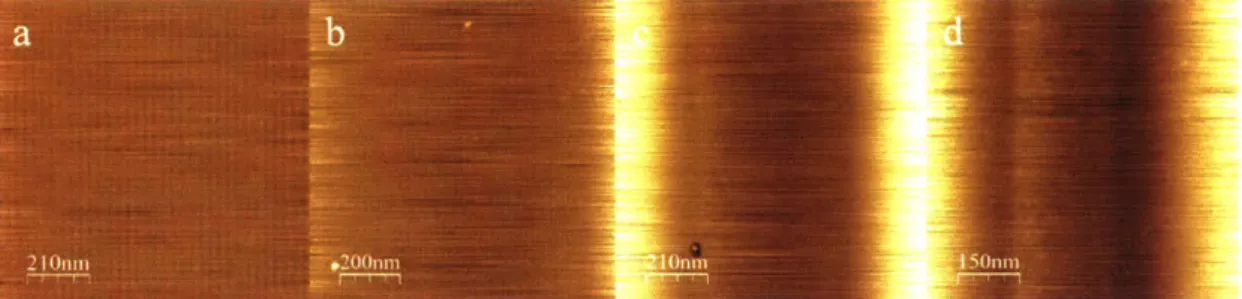
A-1 1 pm2
AFM scans of helium ion beam patterning with different pitches. The array of patterned lines goes from left to right. Each line is etched from top to bottom. The horizontal artifacts are AFM noise. (a-d) Helium ion dosages at 30 keV. (a) 30 nm, (b) 20 nm, (c) 10 nm, and
(d) 5 nm. The smallest resolvable pitch in the AFM was 20 nm. The
white/brigther regions in (c) and (d) are due to the smaller area that was patterned as the pitch was decreased and thus smaller regions of
the h-BN were patterned. Since the same number of etched lines was
A-2 AFM with the precise location of all photo-thermal spectrums
col-lected. Three different sets of measurements. (d, h, m) Photo-thermal spectrum taken from two different locations on the non-patterned h-BN (left half). (e, i, n) Photo-thermal spectrum taken from six different locations along the thinner region of the h-BN grating, strong SiO2 absorption peak at 1084 cm-'. (f, k, o) Photo-thermal spectrum taken from four different locations along the thicker region of the h-BN grat-ing, strong broad absorption peak at 1084 cm-1 and 1368 cm- 1. (g, 1,
p) Photo-thermal spectrum taken from two different locations on the
non-patterned h-BN (right side). The absorption peaks in (1) and (p) are most likely due to the crystal edges in the non-patterned region. 49
Chapter 1
Introduction
1.1
Proposing a graphene-plasmon-based table-top
X-ray source
Rapid progress in nanofabrication methods has fueled a quest for ultra-compact pho-tonic integrated systems and nanoscale light sources. The prospect of small-footprint, high-quality emitters of short-wavelength radiation is especially exciting due to the importance of extreme ultraviolet and X-ray radiation as research and diagnostic tools in medicine, engineering, and the natural sciences. Specifically, the unique capabil-ities of free and coherent electron X-ray sources allow us to probe and capture the crystal, energy, and electronic structure of solid and living biological matter on the order of a nanometer (10-9 m) and are the only reliable tools available for resolv-ing individual proteins and viruses. Furthermore, ultrafast X-ray sources can capture processes that happen on the order of femtoseconds (10'1 s) such as electrons moving in molecules and solids. Accessing these time and length scales helps us understand viral infections, cell division, photosynthesis, and other processes that are important to biology, human health, energy, and the environment.
Therefore, discovering a compact method for generating coherent X-rays is a long-standing holy grail in modern science and engineering. The wished-for device is commonly referred to as a "table-top X-ray laser". Such a device would revolutionize
many fields of science, by making high-quality X-ray beams affordable to laboratories in academia and industry. Today, high-quality X-ray beams can only be created in immensely expensive and large national facilities, such as synchrotrons or free-electron lasers [1] - facilities like the SLAC National Accelerator Laboratory. We approach the challenge of high-quality X-ray sources from a completely unexpected direction, by taking ideas from the rapidly developing field of graphene nanophotonics. Recent work from the Soljani6 Group has proposed and theoretically demonstrated that graphene, with its ability to support strong electric fields and highly confined surface plasmon polariton (SPP) modes, is a promising platform to realize chip-scale sources [2] generating efficient, highly-directional, and tunable X-ray radiation.
The fabrication and characterization work carried out in this thesis is the first step towards making the nanophotonic components of the first proof-of-principle de-vice. In general, our method makes use of several ground-breaking properties of two-dimensional (2D) materials, specifically graphene, a one-atom thick sheet of carbon, whose discovery in 2004 [3] was recognized with the Nobel Prize in Physics (2010). One astonishing property of graphene is its ability to support extremely confined elec-tromagnetic modes, called graphene surface plasmon polaritons, which we shall refer to as graphene plasmons (GPs). These plasmon polaritons are hybrid modes of light (photons) coupled to the polarizable medium of the electron gas in a metal (in this case graphene), therefore deriving their name "plasmon polaritons". We utilize the GPs in a novel scheme for the generation of X-rays from electron beams in vaccum, with-out the need to accelerate electrons to extremely high energies (relativistic speeds). Contrary to existing methods of X - ray generation, our scheme requires only modest electron energies that are easily achievable in laboratory-scale equipment. Further-more, we suggest a design that modifies the commonly used transmission electron microscope, which already operates in the desired energy range.
Our project has a very ambitious goal and is interdisciplinary in nature, combining nanophotonics and electron beam physics. This unique project requires knowledge from both these two communities and challenges the current paradigm in our attempt to create the first GP table-top X-ray source. Since our proposed concept is at the
intersection of these two usually unrelated disciplines, it is adventurous. However, the theoretical concept behind the idea has been rigorously studied and modeled f2]. We hope that the work included in this thesis, in conjunction with other work from colleagues, will lead to the development of novel ideas and concepts.
1.1.1
State of the art methods for creating X-ray radiation
Wilhelm Rbntgen, who discovered X-ray radiation and was awarded the first Nobel Prize in Physics (1901) had already used X-ray tubes at the end of the 19th century for the production of X-rays. Even after a century, X-ray tubes are still the basis for the technology used for all day-to-day X-ray applications (e.g. dental radiography, X-ray computed tomography). Despite many important improvements, X-ray generation is still based on the same physical principles of conventional X-ray tubes. The drawback of even their most modern extensions is in the low-quality beams they produce, which limits the resolution, the contrast, and the penetration depth in imaging applications. It also means that scanning times have to be longer, amounting to increased radiation exposure. Moreover, the time resolution needed for live imaging of extremely fast processes cannot be reached with X-ray tubes.
For this reason, new kinds of physical principles are studied with the purpose of developing new high-quality X-ray sources [4]. For example, one recent idea is using high-harmonic generation to cause hundreds and even thousands of infrared photons to combine into a single soft-X-ray photon [5]. Still, this solution only pro-duces a very low intensity beam, is limited by its very wide spectrum, and can only reach soft-X-ray frequencies, which are not enough for most applications. So far, all sources that can overcome these limitations have one thing in common: they use electron beams that are accelerated to extremely high energies of ultra-relativistic speeds (-y> 1). These electrons are made to interact with an electromagnetic field that accelerates and decelerates them, causing them to emit radiation. One can describe all such processes with the following equation, which relates the energy of a photon in the interacting electromagnetic field, to the energy of a photon in the emitted
radiation called Nonlinear Thomson Scattering or Inverse Compton Scattering1:
photon energy emitted radiation = 47y2 x photon energy interacting field (11)
Equation 1.1 means that in order for free-electron lasers that use an undulator with a period and wavelength of about 3 cm (40 peV photon), to produce hard-X-rays (>10 keV photon), one needs to accelerate the electron beam to at least 5 GeV
(-y>10,000). Our proposal breaks the fundamental limit imposed by Eq. 1.1 and makes it possible for a much lower (-3 MeV) electron energy to create the same hard-X-ray frequency (photon energy of 20 keV). The method would have several additional advantages, and limitations, which we discuss below. Recently the Soljaei6 Group developed a new relationship to replace equation 1.1:
photon energy emitted radiation = 2n x 72 x photon energy interacting field (1.2)
The factor n is the confinement factor of the electromagnetic field when bounded to a surface as in the case of GPs. Therefore, the high confinement factor (n) of graphene will be of great advantage.
1.1.2
Leveraging graphene plasmons
We now emphasize the new physical principles at the heart of our work: Recent discoveries in graphene plasmonics show exceptionally high momentum and strong confinement of light when it is coupled to graphene monolayers [6-8]. Graphene is a two dimensional array of carbon atoms connected in a hexagonal (honeycomb) lattice. This seemingly simple material was found to have incredible strength [9], extremely high mobility [10, 11], and a large absorption [121 (surprising considering that this is only a single layer of atoms). Thanks to the large confinement factor of GPs we can create a deeply subwavelength periodic grating (-10 nm) that forces electrons into transverse periodic acceleration, causing them to emit X-ray radiation. This is the key premise in a GP table-top X-ray source: it significantly reduces the needed electron energies, providing the missing step for a feasible X-ray source on the small-lab scale, removing the conventional requirement for an extensive acceleration stage
(which today requires a building-sized facility). Instead, we can use an acceleration voltage of a few hundred keV to a few MeV, which is a standard technology available in small, lab-scale instruments. Such electron guns are also found in electron microscopes which are commercially available and are commonly used in universities around the world (and even in some hospitals).
1.1.3
Leveraging standard transmission electron microscopes
By using a standard TEM as a potential source, the project benefits from the
proper-ties of this state-of-the-art instrument: First, it already includes an electron gun and vacuum system. Second, the TEM gives us a high-quality beam control, and a simple usage scheme. Third, it is already equipped with the needed X-ray detector (although intended for completely different purposes). Substituting actual parameters in Eq. 1.2 (acceleration of 200 keV that is available in four TEMs at MIT, together with the n~--'200 of GPs, and a photon energy of -1eV for near infrared laser frequencies), we obtain emitted radiation of 400 eV. This value is already in the X-ray range and falls exactly inside the water transparency window (important for imaging of biological samples and for a variety of medical applications). Furthermore, several variations are possible for reaching higher X-ray energies: using larger acceleration values (avail-able in special TEMs reaching ~2 MeV, or in plasma physics groups working with RF guns). We would like to emphasize the crucial advantage of using a TEM here: It is a standard technology, lab-size, and reasonably priced (-$1M). Making small modifi-cations that transform a part of this system into a coherent X-ray source would be a true revolution in X-ray sources. In particular, compared to billion-dollar accelerator facilities, a TEM can be operated in hospitals and can open up extremely valuable imaging tools.
1.2
Introduction: Graphene plasmons
Graphene has recently been presented as en exciting platform for infrared metamate-rials, photonics, and transformation optical devices. Graphene presents three
advan-tages compared to other plasmons materials (i) the propagation length of graphene surface plasmons is longer then in metals [131, (ii) the plasmon is highly confined, theoretically up to 300 times the free space wavelength [6], and (iii) graphene plas-mons can be tuned by chemical or electrostatic doping [14]. These three advantages provide a powerful platform to explore GPs and their applications.
The complex surface conductivity of graphene u = Re(-g) + iIm(ug) depends on the angular frequency w, the chemical potential pM, and the charged particle scattering rate F which is computed from the Kubo Formula [15]. The imaginary part of the of the conductivity has negative or positive values depending on the chemical doping. When Im(u-) > 0 the graphene layer becomes an effective metal layer that can sustain transverse-magnetic (TM) SPP waves. The dispersion relation for the TM wave is
#2
= ko[1 - (2/rmoug)2 ] where 3 and ko represent the wave number of the respectiveguided mode and free space mode. Note that when Im(og) < 0 the graphene layer can no longer support a TM wave.
The propagation length of the graphene plasmon is defined as 1/Im() while the lateral extent of the mode is proportional to 1/Re(O) which for graphene is favor-able over gold or silver plasmons. The real part of 0 for the TM mode along the graphene sheet is much larger than the free space wave number ko = w(Ioco)1/2
. The
confinement factor nspp = Osgp/ko can be greater than 100 and is usually an order
of magnitude more confined then metal plasmons.
The Kubo Forumla provides the expression for the conductivity
_ e2(W + iT- 1) 1 OF(E) _ OF(-E) de
- iirh2 (+ iT-1)2Jo OE F(-e) - F(E) d] (1.3) 10 W + ir-1)2 - 4(E/h)2 =intra + ginter For (y, >> kbT)
-intra + 0-inter = -- +i K 2/2 tci + ( e 2)in h(w. ij-)- 2PC (1.4)
4h fh2( + Iir-1) (47h) h( + r-1) - 2pc + 2pc.
Note that the real and imaginary part, Re(o-,) and Im(o-), are dependent on the chemical doping. Recent experiments, have indeed demonstrated n of 100 [161 and doping of up to 0.9 eV [17], therefore, there is a very flexible range of plasmon excitation to work with. To provide the necessary momentum matching for the wave vectors, either the graphene must be patterned into nano resonators or it must be placed on top of a substrate with a local and periodic change in the permittivity (i.e. grating). If the reader is interested in a more in depth review of graphene plasmonics, they are suggested to read the excellent reviews by Grigorenko et al. [18], Jablan et al. [19], Garcia de Abajo [201, and Low and Avouris [211. We next describe our efforts to create an h-BN grating that can be potentially used to couple into graphene plasmons.
1.3
Introduction: Motivations for h-BN nanoscale
gratings
Light-matter interactions such as absorption and scattering can change drastically once materials are structured at the nanoscale; this is especially true for atomically thin van der Waals materials. Generally, defects are inevitable during nanoscale pat-terning. Therefore, it becomes crucial to understand how nanoscale patterning can introduce defects that modify the electrical, optical, thermal, and mechanical proper-ties of these novel materials. Of particular interest is hexagonal boron nitride (h-BN) which is an ideal substrate for preserving the optical and electronic properties of graphene and most other two-dimensional (2D) materials and nanotubes [22-25]. On its own merit, h-BN is an exciting platform to study new regimes of light-matter inter-actions for highly confined hyperbolic phonon polaritons (HPPs) [26,27], hybridized surface-phonon-plasmon polaritons 128-301, sub-diffractional focusing and imaging [31-34], control over forbidden transitions [35], and as a single-photon emitter via atom-like defects [36]. Many of these properties will benefit from near atomic-scale engineering. Equally as exciting is the creation of van der Waals heterostructures
composed of h-BN, graphene, and other 2D materials to engineer new hybrid proper-ties [37,381 beyond what can be achieved using traditional bulk materials or just one type of 2D material.
To fully exploit the exciting properties of 2D materials and subsequent van der Waals heterostructures, we must be able to tailor the structures at or near the atomic scale. Recently, neon ion beam lithography has been presented as a method of creating nanostructures beyond the reach of most nanofabrication techniques such as electron-beam lithography [39] which is often limited by spot size and interaction volume with the sample. Moreover, the interaction of ion beams with 2D materials such as graphene [401 and subsequent defect control and electronic doping in graphene [41] has been studied as well as the patterning of monolayer graphene [42-45] and MoS2 via a helium ion beam [46]. However, high-resolution and large-area nanoscale
patterning of multilayer and insulating van der Waals crystals such as h-BN is even more challenging and yet to be demonstrated. These nanoscale patterning techniques become important when trying to create useful van der Waals heterstructures, i.e.
h-BN based gratings to couple in and out graphene plasmons in the far-field
[16,47-49] or locally tuning the energy distribution or propagation of graphene plasmons via engineered substrates [50]. To our knowledge, there have been no studies that provide a comprehensive understanding of high-resolution helium and neon ion beam patterning in a 2D material and how subsequent nanostructuring and defects affect light-matter interactions in h-BN nanostructures. These aforementioned issues must be studied and resolved if the advantages of direct and high-resolution ion beam patterning are to be implemented for tailoring van der Waals heterostructures at the near atomic-scale.
In this thesis, we present high-resolution patterning of h-BN with individual fea-ture sizes down to 20 nm and, equally as important, correlate far-field Raman mea-surements to near-field scanning probe based spectroscopy and imaging. We demon-strate that both photo-thermal and scattering-type scanning near-field optical mi-croscopy (s-SNOM) [7,8,26, 51] are required to elucidate the influence of nanostruc-turing on absorption, scattering, and subsequent photo-thermal expansion mediated
through phonons in h-BN. Specifically, we demonstrate geometry and layer dependent photo-thermal expansion of h-BN nanostructures. These measurements provide a full understanding of h-BN nanoscale gratings and what unexpected effects we might see once graphene and other 2D materials are mechanically transferred on top.
Chapter 2
Fabrication and characterization of
h-BN gratings
Multilayer h-BN flakes were prepared by the standard exfoliation process from bulk
h-BN crystals [52]. The h-BN samples were annealed to remove organic contamina-tion before being exposed to either the helium or neon ion patterning process (see Appendix A: Methods). Figure 2-1(a) illustrates an energetic ion sputtering a h-BN layer. Both the helium and neon ion patterning was performed with a Zeiss Orion NanoFab system at the optimal accelerating voltages for high-resolution patterning. An ion dosage sweep was conducted with a grating pattern with a 30 nm pitch. Nanoscale patterning in h-BN flakes can be observed by a change in optical contrast in the exposed regions before and after patterning, Fig. 2-1(b-c). The ion dosages
for both helium, Fig. 2-1(d-g), and neon, Fig. 2-1(h-k), were varied between 1,000
pC/cm and 40,000 pC/cm to determine the optimal dosage for nanoscale patterning. Figures 2-1(f-g) demonstrate that the helium ion dosage at 20,000 pC/cm and 40,000 pC/cm clearly defined the pattern. Figures 2-1(h-k) demonstrate that all dosages for the neon ion beam defined the pattern. Neon ion dosages of
1,000 pC/cm and 10,000 pC/cm uniformly patterned the surface without introducing
undesired surface roughness. At and above 20,000 pC/cm, the h-BN surface devel-oped undulations in height due to the increased sputtering and number of secondary ions created during the recoil of ions in the sample. An additional mechanism could
be neon gas bubbles trapped inside the flake/substrate.
2.0.1
Monte Carlo simulations
To understand the interaction mechanisms between the different bombarded ions and the h-BN sample, Monte Carlo simulations were performed using the TRIM software package [531. The simulation for helium (Fig. 2-2(a)) shows that the majority of the ions passed through the h-BN with minimal interactions. Therefore, the majority of the ion energy was deposited onto the underlying SiO2/Si. When compared to helium, the neon ions had a greater interaction with the h-BN (Fig. 2-2(b)) and therefore transferred a greater amount of ion energy to the h-BN lattice - resulting in a higher sputtering yield. These simulations confirm the experimental results depicted in Fig. 2-1. In Fig. 2-2(c and d), the plots of atomic distributions estimate the number of lattice ions that undergo recoil at each specific target depth. Multiplying the ratio
by the ion dose (units of atoms/cm2), the ordinate of the plot is converted directly into a density distribution (units of atoms/cm3). Even though neon ions have a relatively small interaction volume, their large ion mass allows for a substantial transfer of energy and thus a high sputtering yield (explaining why the neon ion causes over 10x more boron and nitrogen ions to undergo recoil within the sample when compared to helium). In terms of high-resolution patterning, neon ions provide the best balance between resolution and sputtering ability. These results should be taken into account when patterning other crystalline non-conductive materials such as diamond which has become important for quantum communication applications.
2.0.2
Characterization of h-BN grating
2.0.3
Atomic force microscopy
Once an optimal range for the neon ion dosage was determined, a h-BN grating with a 35 nm pitch was fabricated over a 20 pim2 area (dosage of 2000 pC/cm which is equivalent to ~12 ions/nm, all other parameters were the same). The 20 pm2 pattern could be observed in optical microscopy (Fig. 2-3(a)). The difference in
optical contrast between the left and right half of the grating is due to a variation in the thickness within some regions of the pre-patterned flake. These topographical variations are explained next and the subsequent effects on the optical properties of these h-BN nanostructures are discussed later. Atomic force microscopy (AFM) of the pattern was done to understand the exact features milled into the h-BN (Fig.
2-3(b-c)). The AFM in Fig. 2-3(b) shows the bottom right corner of the grating in
Fig. 2-3(a). These scans show crystal step-edges in the middle and the bottom, which were created due to an uneven exfoliation process. These step-edges allow us to study the nanopatterning influence on a range of h-BN thicknesses. A high-resolution AFM scan (using a tip with a 7 nm radius) was performed in the middle of the grating to reach the bottom of the etched features (Fig. 2-3(c)). The cross-section in Fig. 2-3(d) demonstrates the overall height profile of the entire grating. The left half (thinner region) of the h-BN grating had an average height of ~25 nm, while the right half (thicker region) of the h-BN grating had an average height of ~45 nm. The gradual change of h-BN thickness on the right half of the flake contributed to drastic and random nanostructuring of the h-BN because step-edges were directly exposed to the neon ion beam. These exposed edges provided a jagged template leading to variations of up to -20 nm in height after patterning (as opposed to the uniform patterning on the left half of the grating). Figure 2-3(e) shows the cross-section of the high-resolution AFM depicted in Fig. 2-3(c). We highlight that the semi-flat region at the bottom of each nanostructure confirms that the AFM tip was able to reach the bottom of each etched feature. The profile demonstrates that the neon ion beam was able to mill a depth between 6-8 nm with individual h-BN nanostructures ~20 nm wide over the entire 20 pm2 area.
2.0.4
Raman spectroscopy
To understand the effects of the nanopatterning on the crystal structure of h-BN, Raman spectroscopy was used to observe the optically active phonons and subse-quent disorder introduced at the nanoscale. Previous Raman spectroscopy of h-BN has demonstrated a characteristic peak for the E2g in-plane phonon mode [54-561
at 1366 cm-1. Fig. 2-4 demonstrates the optical image of the h-BN grating with the corresponding Raman spectrum and maps that distinguish vibrational modes in the sample. Figure 2-4(b) shows the Raman spectrum measured from three dif-ferent regions: the non-patterend h-BN, thicker grating region, and thinner grating region. Zoom-in spectrums of the thinner and thicker regions are shown in Fig. 2-4(c) demonstrating that the h-BN peak is twice as strong in the thicker region compared to the thinner region. Figures 2-4(d-f) show the Raman maps with the value of the integrated area under each corresponding peak within the ranges 1340-1390 cm-1,
1425-1475 cm- 1, and 1540-1570 cm-1
. As seen from the Raman spectrum and map, the h-BN phonon peak at 1366 cm-1 was sharp and unmodified in the non-patterned region of h-BN and decreased significantly as the Raman scan moved from the edge and into the grating. Specifically, there was a ~48 times reduction of the Raman intensity in the thicker region and -227 times reduction in the thinner region. This result might be partially expected due to the difference in sample thickness observed in the optical microscopy and AFM. In Fig. 2-4(e), the Raman peak of the third order silicon TO phonon [57, 58] at 1450 cm- grew stronger in intensity as the scan moved from the edge and into the grating. Moreover, the signal of the silicon TO phonon was stronger in the thinner region compared to the thicker region. The signal from the TO phonon was most likely strongest in the regions where the ion milling of the
h-BN exposed more of the silicon to the laser, thus providing a stronger Raman
sig-nal. Lastly, in Fig. 2-4(f), a Raman peak at 1550 cm- 1 is most likely due to ambient oxygen as recently reported for related experiments
1591.
There are at least three possible reasons for the reduction of the Raman signal for the h-BN phonon at 1366 cm-1. First, a reduction normally indicates a high degree of surface and boundary defects that affects the phonons in the h-BN. Moreover, the Ne+ ion interstitials within the plane or between the h-BN layers could further modify the vibrational modes (phonon dispersion). Another possible contribution to the weaker Raman signal could be a reduced coupling efficiency of the Raman laser due to increased light scattering from the grating. Since this is a far-field measurement, the information obtained about the h-BN structures (and phonons) at the nanoscale
could be limited; therefore, it is necessary to use nano-imaging and spectroscopy
techniques that provide complimentary and necessary information about the way
these materials are engineered at the nanoscale before they can be used in any type
of engineered van der Waals heterostructures.
-j
Ion Beam
Pattern
a b c
Helium Ion Dosage Test
d
e
f
g
Neon Ion Dosage Test
h
jk
Figure 2-1: Hexagonal boron nitride nanopatterning. (a) Illustration of nano
patterning due to ion bombardment.
(b, c) Optical micrograph before and
af-ter ion beam pataf-terning.
Helium versus neon ion dosage. Atomic force
mi-croscope scans of (d-g).
The array of patterned lines goes from left to right.
Each line is etched from top to bottom. The horizontal artifacts are AFM noise.
Helium ion dosages at 30 keV. (d) 1,000 pC/cm.
(e) 10,000 pC/cm. (f) 20,000
pC/cm. (g) 40,000 pC/cm. Helium dosages between 20,000 and 40,000 pC/cm
clearly defined the pattern. (h-k) Neon ion dosages at 25 ke V. (h) 1,000 pC/cm.
(i) 10,000 pC/cm.
(j)
20,000 pC/cm. (k) 40,000 pC/cm. Neon dosages between 1,000
30 keV Helium
OuD -:,910 NATMDSMMN
33 Ke-! Ditnbutiyn U AI
b
d
*1 U U) 3 0 .4 U) if Ii U) 3 a I-.4 -lies hMOS 1013w Ewes0 Sios' 9g3*5 0 1A25 keV Neon
910p
CS
ATOM DISTRIBUTIONS D Rftuil Dntibtnn n~ R~r) Dsirnbum-.~k
ReU fl~nbglmanFigure 2-2: Monte Carlo simulations of ion trajectories. Simulations
compar-ing the range and trajectory of (a) 30 keV He ions in a 56.5 nm-thick h-BN and (b)
25 keV Ne ions in a 45 nm-thick h-BN on top of the SiO2/Si substrate. (c-d) Atomic
distributions for each simulation provide the number of ions that undergo recoil at
a specific ion dosage. The Ne ion causes over 10x more boron and nitrogen ions to
undergo recoil. In collaboration with David C. Bell, Center for Nanoscale Systems,
Harvard University.
31
a
C
U U) a C .4 '3 S U) 3 C I-.4 . ! I.
A - TWOWe Degt& - Aa
d 50 ' 40 30 120 10 0 b 0 5 10 Length [rm] 15 20C
0LM
CD 1, 15 10 5 0 0 100 200 300 Length [nm]Figure 2-3: Hexagonal boron nitride grating with optimal neon dosage.
(a) Optical image of a 20 pm
2h-BN grating fabricated via neon ion beam patterning
at 25 keV. The difference in optical contrast is due to a gradient in height. (b-c)
AFM scans of the h-BN grating. (b) 10 1m
2scan of bottom right corner in Fig.
2-3(a) denoted by the white dashed box. (c) High-resolution 1 11m
2scan of the milled
pattern (using a 7 nm tip radius). (d) Cross-section of the entire grating which is
represented by the blue dashed line in Fig. 2-3(a). (e) Cross-section of the 1 Jim
2scan
confirming a pitch of 35 nm, a mill depth between 6-8 nm, and a nanostructure width
of ~20 nm.
a
10 Optical b 5 0L -5 -10 -5 0 5 10 x [pm] 1335-1395cm '1 d 10 e -10 -10 -5 0 5 10 x [pm] 10000 8000 6000 o 4000 2000-| I thinner 1366 cm -thicker --- non-patterend 1556 cm-01 1200 1300 1400 1500 Wavenumber [cm~ ] 14?0-1480 rem~11 f 10 5 0 -5 -10 -10 -5 0 5 10 x [pm] 800 ... thinner C 700 -thicker 600 =i500 0 400 o0300. 00 200 1200 1300 1400 1500 Wavenumber [cm ] 1545-1565 [cm-] 10 -10 -10 -5 0 5 10 x [pm]Figure 2-4: Raman spectroscopy and Raman maps. (a) Optical image of the
h-BN grating. (b) Raman spectrum comparing locations inside and outside the grating
region. Plot includes h-BN phonon mode at 1366 cm-1, third order silicon TO phonon
at 1450 cm-
1, and ambient oxygen at 1556 cm-
1. (c) Plot of Raman spectrum inside
the thinner and thicker regions of the grating. (d-e) Raman maps showing the value
of the integrated area under the peaks found within the ranges 1340-1390 cm-1,
1425-1475 cm-1, and 1540-1570 cm-
1. All maps are normalized to the maximum counts
found within each range. (d) Intensity map of the h-BN phonon peak at 1366 cm-.
(e) Intensity map of the silicon TO phonon at 1450 cm-1. (f) Intensity map of peak
Chapter 3
Scanning probe microscopy of h-BN
gratings
3.0.5
Photo-thermal spectroscopy and imaging
To better understand how the nanoscale patterning affected the absorption of light and the coupling to the phonons in h-BN, photo-thermal spectroscopy and imaging were performed using an Anasys nanoIR2-S. We show a schematic of the microscopy setup in Fig. 3-1(a). The h-BN sample was illuminated with pulsed infrared light with angular frequency WL from an optical parametric oscillator. A gold-coated AFM tip in contact mode is used to detect local thermal expansion of the sample caused by the absorption of the incident light. The mechanical expansion of the sample excites the mechanical resonances of the AFM cantilever and the measured amplitude of oscillation is directly proportional to the sample absorption. In this experiment, the absorption peaks correspond to the excitation of phonons in both the h-BN and the SiO2/Si substrate and subsequently provide a chemical signature at the nanoscale. Figure 3-1(c-d) show the IR spectrum taken from various points in both the thinner (left side) and thicker (right side) regions of the h-BN grating respectively (cross-section shown in Fig. 2-3(d)). Figure 3-1(d) shows an absorption peak for the TO optical phonon of the SiO2 [60,611 at 1084 cm-1 only inside the thinner region of the
the Appendix A:Methods for multiple measurements). This peak arises because the removal of the top h-BN layers during the ion milling provided increased coupling to the SiO2 underneath (recall that the left region is ~20 nm thinner than the thicker
region and that the tip is assumed to have a radially symmetric field). In Fig. 3-1(c) a strong and broad absorption peak at 1368 cm- 1 corresponding to the TO optical phonon in h-BN is measured for all points inside the thicker region of the grating - we note that this same region has a higher number of layers and more pronounced topographical peaks and valleys compared to the thinner region. The point-to-point spectroscopic differences within the h-BN grating were suggested in the Raman spectrums, but the differences in the photo-thermal spectrum were more substantial and clear with the near-field technique.
Direct photo-thermal imaging was conducted for the top right of the grating, AFM shown in Fig. 3-1(e). Figures 3-1(f and g) demonstrate the photo-thermal images collected by scanning the tip while illuminating the sample with one specific wavelength of light. This same photo-thermal microscopy setup was recently used for the pure mechanical detection of HPPs in h-BN by Ambrosio et al [61]. The respective wavenumbers (wavelengths) chosen in Fig. 3-1(f and g) were 1368 cm-1
and 1600 cm- 1 (off the optical phonon resonance). The photo-thermal image at
1368 cm-1 shows a clear and strong absorption peak at the phonon mode. This indicates that the photo-thermal technique can excite and couple to the phonons in the lattice and subsequently measure the mechanical expansion of the nanostructured
h-BN due to the absorption of light.
We first note that although the Raman signal for the h-BN phonon mode at
1368 cm- 1 inside the thicker region of the grating is reduced by an order of magnitude (~48 times smaller), the photo-thermal response inside the grating is increased by an order of magnitude (~17 times larger) when compared to the non-patterend
h-BN. Normally a weak Raman signal depicts substantial defects and strong disorder
in a 2D crystalline lattice (as frequently observed in graphene [62, 631 which often leads to decreased light absorption. However, in this case, although the Raman signal inside the grating region is very weak, the photo-thermal measurement shows
strong absorption at the phonon resonance, which demonstrates that the lattice is not completely disordered by the ion beam nanostructuring.
By examining the cross-section and the topography of the grating, we conclude
that the above result is a combination of effects: (i) Stronger near-field coupling due to the roughness of the surface, which strongly interacts with an AFM tip in the photo-thermal, but did not interact as strongly with the far-field of the Raman laser. This interaction then transferred energy to the phonon modes of the unperturbed h-BN layers beneath the surface. (ii) It may be that the phonon dispersion of the h-BN was modified by the nanopatterning, which caused a modification of the measurements. (iii) The sharp and pronounced geometry of the h-BN nanopatterns caused stronger thermal expansion. In any casc, it is likely that the h-BN layers beneath the top few nanometers of the flake were mostly protected from the ion milling process and obtained minimal damage.
Let us elaborate on the last mechanism above: the confinement of the phonons and the subsequent increased heat in the h-BN regions were more pronounced where sharper peaks and valleys were located in the AFM image. This can be explained because the extreme anisotropy of the h-BN lattice, which contributes to its hyper-bolic optical properties [31], also results in a drastic difference between the thermal expansion coefficient in the a-direction (basal plane) and the c-direction (orthogonal to the basal plane). Specifically, it has a large and positive thermal expansion coef-ficient of 38 x 10-6/K in the c-direction [641 (as opposed to the small and negative coefficient -2.7 x 10~'/K in the a-direction). Originally emphasized by Lifshits, the in-creased absorption of light (and subsequent heating) in this highly anisotropic crystal leads to acoustic "bending" waves [65] which causes the significant expansion in the c-direction and contraction in the a-direction. This mechanism has been theoretically and experimentally investigated for other bulk layered crystals such as GaS, GaSe, and InSe [66]. Moreover, in these nanostructures, the reduction of bonds in the basal plane may allow the crystal to contract further in the basal plane and thus conserve its volume by expanding in the c-direction, further contributing to the strong photo-thermal signal. Since this specific photo-photo-thermal technique has only been recently
been used to study atomically thin van der Waals materials, we employed the use of a complimentary scanning probe microscopy to ensure that anomalous tip interactions were ruled out as the main reason for these large absorption values.
3.0.6
Scattering-type scanning near-field optical microscopy
Thus, to further understand the relationship between patterning, defects, and the interaction with light, infrared nano-imaging experiments were conducted using a neaspec s-SNOM. The measurements were taken of the entire h-BN grating and of zoomed-in regions at 1368 cm- 1 and 1425 cm 1 respectively to understand how the phonon vibrations, and any possible HPPs, were modified by the nanopatterning. Figure 3-2(a) depicts the AFM of the entire h-BN grating. The respective s-SNOM images in Fig. 3-2(b and c) show a stronger scattered light signal from the thicker and sharper nanostructured areas on the right half of the grating (similar to the stronger absorption signal from the photo-thermal microscopy in Fig. 3-1.) Figures 3-2(d-f) demonstrate zoomed-in topographic and s-SNOM images of the 3 Pm2 area in the re-spective white dashed boxes in Fig. 3-2(a-c). For both sets of s-SNOM measurements, the AFM tip clearly distinguished the topography of the patterned h-BN while collect-ing a stronger scattercollect-ing-amplitude from the areas that had taller and more drastic changes in topographic height. The difference in measured amplitudes within the grating may be partially due to the difference in the number of layers underneath each measured point. For the zoomed-in measurements, it may be that the -10 nm tip may be too large to fully interact with the bottom of each individual nanostruc-ture (as opposed to a high-resolution tip). Nevertheless, the stronger signal from the thicker side of the grating can not be solely attributed to poor tip interactions because the right side of the grating also has the 6-8 nm trenches on top of the drastic valley and trough like structures seen in the previous AFM cross-sections. Nevertheless, propagating phonon polaritons in the non-patterned regions are clearly seen at 1425
cm 1 as previously demonstrated by Dai et al [26]. The observation of these prop-agating phonon polaritons in the window (non-patterned) region confirms the high quality of the original h-BN flakes and rules out any contamination or unintentional
surface modification as causing the increased photo-thermal or scattering signal from
the grating. We note that these HPPs were not observed with the photo-thermal
microscope (Fig. 3-1) due to the lower signal strength of the illumination/detection
technique. Lastly, one can only speculate that different effects happen within the
grating such as nearest neighbor coupling between individual nanoresonators or that
the protected layers underneath could still sustain HPPs, but that would require a
systematic study of nanostructure geometry, grating pitch, and layer thickness that
is beyond the intent of this initial study.
Both the photo-thermal imaging and s-SNOM techniques detected the difference
in absorption and scattering due to number of layers and geometry of the h-BN
sample. We emphasize that although both scanning probe techniques use similar
metalized AFM tips, components, and tunable infrared lasers, the mechanism of
detection for photo-thermal imaging is substantially different from s-SNOM. Instead
of detecting scattered light, photo-thermal microscopy uses a tip in contact mode and
detects absorption through the pure mechanical expansion of the sample. Regardless
of the techniques, both the photo-thermal and s-SNOM techniques are powerful and
complimentary ways of studying how light interactions (absorption and scattering)
are modified in nanoengineered h-BN and other van der Waals materials. It should be
of great interest to note that these same photo-thermal expansion properties should
be experimentally verifiable and tuned in 2D crystals of GaS, GaSe, and InSe which
have only been very recently explored [67,68].
t lQuadrant detector
400" Tuned pulsed
lR laser (L)
Photo-thermal signal Patterend hBN -Thicker Region
20 C [--Ppt ] pt 41 15. -Pt51 0 0 0 1000 1200 1400 1600 Wavenumber [cm
4]
d20 Patterend hBN -Thinner Region ~~t 9 I-Pt 101 I Pt ill 15 -W10 5 0 1000 1200 1400 1600 Wavenumber [cm *]
g
? 9 13.34 20.01 6.67 13.34 20.01Figure
3-1:
Photo
-
thermal infrared spectroscopy and imaging.
(a)
Schematic of photo-thermal illumination/detection system (b) AFM image with the
location of all photo-thermal (absorption) spectrums taken. Numbers correspond
to locations of the plotted spectrums.
(c) Photo-thermal spectrums taken from
four different locations along the thicker region of the h-BN grating, strong and
broad h-BN absorption peak at -1368 cm-
1. (d) Photo-thermal spectrum taken
from four different locations along the thinner region of the h-BN grating showing
a strong SiO
2absorption peak at -1084 cm-
1. Photo-thermal Imaging (e) AFM
image of the top right corner of the h-BN grating indicated by the white dashed box
in Fig. 3-1(b). (f) Photo-thermal image of the top right corner at 1368 cm-
1. (g)
Photo-thermal image of the same region at 1600 cm-
1.
a
b 0 f 6.67 13.14 Deflection laser10
(wn 0 30 20.01a
b CTopography 1368 cm- 1425 cm-1
d ef
-Topography 1368 cm-1 1425 cm-1
Figure 3-2: s
-
SNOM. (a) Topography scan taken of the entire grating structure.
(b) s-SNOM image taken at 1368 cm-
1. (c) s-SNOM image taken at 1425 cm-'. (d)
zoomed-in 3
llm2topography scan, region highlighted by the white box in Fig. 3-2(a).
(e) 3 urM
2s-SNOM image taken at 1368 cm-1. (f) 3 pm
2s-SNOM image taken at
1425 cm-
1. In collaboration with Siyuan Dai, Department of Physics, University of
Chapter 4
Conclusion
In summary, we for the first time demonstrated that high-resolution ion beam nanoscale patterning of multilayer van der Waals materials (in this case h-BN) is possible and provides a way of modifying the properties of the materials at the nanoscale. More-over, we show that neon is a better candidate compared to helium for direct high-resolution patterning of insulating van der Waals materials. We note that although Raman spectroscopy of the nanostructured h-BN provides information of the ac-tive phonons in the material, it can not completely predict and elucidate the full optical response of nanostructured materials in the near-field. For this reason, we used photo-thermal spectroscopy and imaging on a nanopatterned crystalline van der Waals material, demonstrated layer and geometry dependent photo-thermal response, and noted the role of extreme anisotropies and large positive expansion coefficients in the photo-thermal expansion of the sample. This work provides a baseline for the continued exploration of near atom-scale patterning of van der Waals materials with ion beams. It shows that nanopatterning techniques and the correlated far-field and near-field characterization techniques will be especially important as van der Waals heterostructures are explored and engineered with nanoscale precision.