HAL Id: hal-00175317
https://hal.archives-ouvertes.fr/hal-00175317
Submitted on 18 Jun 2019
HAL is a multi-disciplinary open access
archive for the deposit and dissemination of
sci-entific research documents, whether they are
pub-lished or not. The documents may come from
teaching and research institutions in France or
abroad, or from public or private research centers.
L’archive ouverte pluridisciplinaire HAL, est
destinée au dépôt et à la diffusion de documents
scientifiques de niveau recherche, publiés ou non,
émanant des établissements d’enseignement et de
recherche français ou étrangers, des laboratoires
publics ou privés.
Few layer graphene on SiC, pyrolitic graphite and
graphene: a Raman scattering study
Clément Faugeras, Anouck Nerrière, Marek Potemski, Ather Mahmood, Erik
Dujardin, Claire Berger, Walter de Heer
To cite this version:
Clément Faugeras, Anouck Nerrière, Marek Potemski, Ather Mahmood, Erik Dujardin, et al.. Few
layer graphene on SiC, pyrolitic graphite and graphene: a Raman scattering study. Applied Physics
Letters, American Institute of Physics, 2008, 92, pp.011914. �10.1063/1.2828975�. �hal-00175317�
arXiv:0709.2538v4 [cond-mat.mes-hall] 7 Dec 2007
study
C. Faugeras,1, ∗A. Nerri`ere,1M. Potemski,1A Mahmood,2 E. Dujardin,2 C. Berger ,3 and W. A. de Heer 3
1
Grenoble High Magnetic Field Laboratory, CNRS, 38042 Grenoble, France
2
CEMES, CNRS, 31055 Toulouse, France
3
Georgia Institute of Technology, Atlanta, Georgia, USA
The results of micro-Raman scattering measurements performed on three different “graphitic” materials: micro-structured disks of highly oriented pyrolytic graphite, graphene multi-layers ther-mally decomposed from carbon terminated surface of 4H-SiC and an exfoliated graphene monolayer are presented. Despite its multi-layer character, most parts of the surface of the graphitized SiC substrates shows a single-component, Lorentzian shape, double resonance Raman feature in strik-ing similarity to the case of a sstrik-ingle graphene monolayer. Our observation suggests a very weak electronic coupling between graphitic layers on the SiC surface, which therefore can be considered to be graphene multi-layers with a simple (Dirac-like) band structure.
The interest in the properties of graphite-like al-lotropes of carbon has recently been rekindled when its simplest form, graphene, a mono layer of carbon atoms arranged in a honey comb lattice, was experimentally identified and readily produced by a simple exfoliation technique1. The linear dispersion at the K and K’ points
of the graphene band structure gives rise to a relativistic-like behavior of free carriers that has many implications for the observed quantum mechanical effects, such as the half-integer quantum Hall effect, and has stimulated con-siderable research over the past few years2,3,4.
Alterna-tively, thin graphitic layers can be epitaxially grown on 4H-SiC substrate5,6, by the thermal decomposition of
ei-ther Si- or C-terminated surface. In this case, the ma-terial, herein referred to as few-layer graphene (FLG) on SiC, may be composed of one or many graphene layers, depending on the growth conditions. Although much in-teresting physics has emerged from the studies of exfoli-ated graphene structures, the epitaxy of graphene seems to be the most viable production route for electronic applications4.
In this letter, we present the results of micro-Raman scattering studies of few-layer graphene on C-terminated surface of SiC (FLG-C-SiC) with a large number of lay-ers, and compare them with the data obtained on disks made of highly oriented pyrolitic graphite (HOPG) with different thicknesses and with the spectra of an exfoli-ated graphene monolayer. Attention is focused on the form of the so called D’-band, a well established fea-ture in the Raman scattering spectra of graphite7 and
graphene8,9,10. Its single-component form is the
finger-print of the simple electronic bands in a graphene mono-layer, while a multi-component form is the signature of the complex band structure of multi-layers with Bernal-type (graphite-like) stacking.
Apart from some residual inclusions, most of the sur-face of the FLG-C-SiC probed with micro-Raman spec-troscopy was found to show a single component D’ fea-ture, as for an exfoliated graphene monolayer but in striking contrast to the double-component D’-feature ob-served in HOPG disks. This observation supports the
view that FLG-C-SiC is a system which displays single band (Dirac-like) dispersion relation of electronic states characteristic of decoupled graphene layers.
The structures used for experiments were disks of HOPG with different thickness, an exfoliated graphene monolayer, and, three FLG-C-SiC samples with a dif-ferent number of layers. HOPG disks (20-µm in diame-ter) have been prepared by mechanical cleavage with a pulled glass tip of cylindrical ZYA grade HOPG mesas and by deposition via micro-manipulation onto a sili-con substrate with a 100-nm or 300-nm SiO2 layer11,12.
Graphitic disks could be further thinned by exfolia-tion down to a thickness ranging between 2 and 20 nm. A graphene monolayer was prepared by exfolia-tion of freshly cleaved ZYA grade HOPG on a silicon substrate with a 300 nm thermal oxide substrate as de-scribed in the literature1. Sub-20 nm thick graphitic
disks and the graphene layer were subsequently charac-terised/identified by AFM. FLG-C-SiC structures were thermally decomposed from 4H-SiC substrates following the procedure detailed in Ref. 5 and 6. Two of them (sample 1 and 2) are 5-10 layers thick while sample 3 consists of 70-90 layers, as determined from the intensity ratio of the Si 92-eV and C 271-eV Auger peaks5. Raman
scattering spectra have been measured using a confocal microscope with 2µm spatial and 1 nm spectral resolu-tion. Experiments were performed at room temperature using the 632.8 nm line of a HeNe laser.
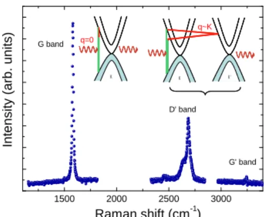
We start the discussion of the experimental results by presenting the characteristic Raman-scattering spectrum of bulk graphite, obtained here for a thick (∼100 nm-high) disk of HOPG (see Fig. 1). The G band at 1582 cm−1is due to first order (one phonon) Raman scattering
process. It is characteristic of sp2 hybridization and
in-volves the in-plane optical phonon E2gnear the Γ point of
the phonon band structure. As a rule, the overtone (two-phonon process) of the G-band, labeled as the G’-band in Fig. 1 is much less intense. The first order Raman scattering process due to characteristic zone boundary phonons (at 1325 cm−1) is forbidden in defect-free
2 1500 2000 2500 3000 K K ‘ K K ‘ KK q~K G' band In te n s it y ( a rb . u n it s ) Raman shift (cm-1) G band D' band q=0
FIG. 1: Raman spectrum of a 20-µm diameter HOPG disk. Inset: Schematics of the first and second order Raman scat-tering processes responsible for the G band and the D’ and G’ bands respectively. The phonon wave vector implied in both scattering processes is indicated in red.
phonons effectively contribute to a double resonance Ra-man scattering process7 (involving two phonons) which
results in the appearance of the characteristic D’ band at ∼2650 cm−1 (under HeNe laser excitation). Such a Ra-man scattering process, schematically shown in the inset of Fig. 1, is inherently sensitive to the multi or single-band character of the dispersion relations of the elec-tronic states. In consequence, the D’-feature is known to be composed of at least two-components in graphite (as seen in Fig. 1) and also in other graphene multi-layers with Bernal stacking due to the multi-band character of the electronic states in these systems. In contrast, the unique single Lorentzian form of the D’-feature is the signature of a system with a single-band electronic dis-persions, such as the representative graphene monolayer. Fig. 2 illustrates the form of the D’-band in Raman scattering spectra measured for our HOPG disks with different thicknesses. A detailed analysis of the observed changes of the form of the D’-band is beyond the scope of this work, nevertheless it is clear that the low energy part of this band gains in intensity when the disk height is reduced down to 2 nm (∼6 graphitic planes). To quantify this change, we assume that this band is a simple superposition of two Lorentzian peaks. The shape of the observed D’ band can be reasonable reproduced assuming the high energy peak is fixed at 2686 cm−1but
the center of the low energy peak shifts from 2636 cm−1
for HOPG to 2653 cm−1 for a 2-nm thick disk. The
ratio of the amplitude of these two peaks can be used to estimate the thickness of the graphite disks (see inset of the Fig. 2). The present experiments performed on graphite with thickness between 2 and 20 nm bridge the current measurement gap between the well-documented bulk graphite7 and recent micro Raman scattering
studies on exfoliated few layer graphene8,9,10.
We turn our attention now to the main topic of this paper which is the investigations of FLG-C-SiC
struc-2400 2500 2600 2700 1 2 3 4 20 10 A m p lit u d e r a ti o Height (nm) 0 HOPG c (17 nm) b (20 nm) a (HOPG) d (15 nm) N o rm a liz e d I n te n s it y ( a rb . u n it s ) Raman shift (cm-1) e (2nm)
FIG. 2: Raman spectra of the D’ feature of (a) HOPG and of 20 µm diameter HOPG thin disks with heights measured by AFM of (b) 20 nm, (c) 17 nm, (d) 15 nm, (e) 2 nm. The solid and dashed lines are Lorentzian fits. These spectra have been normalized to the high energy component of the D’ line to show the observed effect. Inset : Amplitude ratio of the two components of the D’ line as a function of the height of the graphite disk.
tures. Our results of micro Raman scattering studies are summarized in Fig. 3. As a rule, the Raman scattering spectra of these samples show the characteristic G and D’ bands on the background of a more or less pronounced signal from the SiC substrate13, and the spectrum of the
latter is shown for comparison (trace (a) in Fig. 3). When scanning the laser spot over the FLG-C-SiC surface we find that most of the sample gives rise to the character-istic Raman scattering spectra which are shown in Fig. 3 (traces b, c and d), for three different samples. The im-portant feature of these spectra is the appearance of the D’ band in the form of a single component peak. We note, however, the existence of some inclusions or spots on the sample surface, which are visible under an optical microscope, and which give rise to a different spectrum characterized by a distinct, more complex shape of the D’-band (see trace (b’) in Fig. 3).
The Raman scattering spectra of our FLG-C-SiC sam-ples can be compared to the characteristic spectrum of the graphene monolayer (trace (e) in Fig. 3) and/or to the spectra of HOPG disks shown in Fig. 2. Within ex-perimental uncertainty, the energetic position of the G-peak is common for all samples. Not surprisingly, this means that E2g in-plane optical phonons are the same in
all these materials. It is worth noticing that the spectra presented here show no sign of the D-band. This demon-strate the weak disorder in our samples14,15. The D-band
can also appear in the spectra measured at the edges of the graphitic flakes8, but in our experiments the laser
spot was always focused on the interior of the measured structures.
The resemblance of the shape of the D’-band in the Raman scattering signal arising from the majority of the surface of our FLG-C-SiC samples to the D’-band mea-sured on the exfoliated graphene flake is remarkable. A single Lorentzian peak is seen for both type of structures.
1400 1600 2600 2800 e d c b b' SiC exfoliated graphene FLG on SiC Raman shift (cm-1) In te n s it y ( a rb . u n it s ) a
FIG. 3: Raman spectra of a 4H-SiC substrate (a), of a graphitic residue on sample 1 (b’), of 5-10 layers FLG on 4H-SiC substrate (b) for sample 1 and (c) for sample 2, of 70-90 layers epitaxial FLG (d) and of exfoliated graphene (e). The solid lines are Lorentzian fits.
This is particularly clear for the graphene and the FLG-C-SiC samples 1 and 2, each showing the same half-width of 29 cm−1. The fit of the Lorentzian profile to the
D’-line is not as good for the case of sample 3 which has as many ∼90 layers, and results in a larger half-width (D = 40 cm−1). The FLG-C-SiC samples differ however from
graphene as far as the position of the D’-band is con-cerned. In our spectra for exfoliated graphene, this band is centered at 2641 cm−1, whereas the D’-peak of
FLG-C-SiC samples appears at slightly higher energies. Its actual position fluctuates from one location to another of the laser spot on the sample and from sample to sample, but remains in the range 2655 - 2665 cm−1. The
Ra-man scattering signal which arises from the visible inclu-sions on FLG-C-SiC surfaces shows a D’-band of a more complex form. We note the resemblance to the D’-band characteristic of graphite in general, and more precisely to the one observed for our thin HOPG disks. We spec-ulate that this minority Raman scattering signal (linked to the inclusions) originates from some graphitic residues (Bernal-stacked graphene multilayers) on the surface of our FLG-C-SiC. Decomposing the D’-band characteristic of the graphitic residue in samples 1 into two Lorentzian peaks we find that the amplitude ratio of these peaks is the same as in the case of a HOPG disk with a height of ∼3 nm (∼10 monolayers).
The striking correspondence in the shape of the D’-band observed in the majority Raman scattering sig-nal from the FLG-C-SiC samples and from graphene is a clear indication of the similar electronic structures in both these material systems. This strongly supports
pre-vious work pointing towards the quasi-two dimensional Dirac-like character of electronic states in FLG-C-SiC samples6,16. Our results are also consistent with
re-cent reports which illustrate that two dimensional carbon layers on C-face SiC substrates are not Bernal stacked. Instead, these layers are generally rotated at specific angles17, and in consequence are electronically well
de-coupled one with respect to another. To some extent, the FLG-C-SiC resembles the so-called “turbostratic” graphite, also composed of non Bernal-stacked, but ran-domly rotated, layers. A single component D’-band is also characteristic of the “turbostratic” graphite14,15.
The differences in the Raman scattering spectra of FLG-C-SiC and of “turbostratic” graphite are however also clear. “Turbostratic” graphite show much wider D’-peaks (typically 50 cm−1 in Ref. 18) and a visible
D-band, the latter due to the appreciable disorder and/or small size of such graphitic granulates. On the other hand, the D’-peaks in FLG-C-SiC and “turbostratic” graphite are centered at very similar energies, but charac-teristically higher, by about 20 cm−1as compared to the
case of graphene. While the shift of the D’-peak for the FLG-C-SiC (and “turostratic” graphite) as compared to the case of graphene might be due to a difference in the phonon energies characteristic of each of these systems, we speculate it is more likely due to the possible differ-ence in the Fermi-velocity of Dirac cones in these systems. Recent reports clearly show that the energy position of the D’-band, arising from the double resonant Raman scattering process, can depend on the Fermi-velocity and this parameter seems to be ∼ 10% larger for graphene19
compared to FLG-C-SiC16. While no shift is observed
for the G-band, a third possible but unlikely explanation for the observed energy shift of the D’ band could also be a natural doping of the FLG-C-SiC? .
In conclusion, we have found the majority signal of micro-Raman scattering observed from graphitized carbon-terminated surfaces of SiC shows a double res-onant D’-band in the form of a single component peak which indicates the single-band electronic struc-ture of this material. Together with previously re-ported results of transport6, spectroscopic16 and
struc-tural investigations17, the present data confirms the
ap-pearance of Dirac-like electronic states in FLG-C-SiC. Remarkably, this is in spite of its multilayer character. Almost certainly, the layers of FLG-C-SiC are electron-ically well decoupled, as is the case to some extent in “turbostratic” graphite. This suggests that functional graphene-based devices can be developed using the meth-ods of thermal decomposition (epitaxy) of silicon carbide, opening the way for many potential applications.
We gratefully acknowledge E. Bustarret and D.K. Maude for stimulating discussions.
∗ Electronic address: [email protected] 1
4
Jiang and Y. Zhang and S. V. Dubonos and I.V. Grigorieva and A. A. Firsov, Science, 306, 666 (2004).
2
K. S. Novoselov and A. K. Geim and S. V. Morozow and D. Jiang and M. I Katsnelson and I. V. Grigorieva and S. V. Dubonos and A. A. Firsov, Nature, 438, 197 (2005).
3
Y. Zhang and Y.- W. Tan and H. L. Stormer and P. Kim, Nature, 438,201 (2005).
4
A. K. Geim and K. S. Novoselov, Nature Mat., 6, 183 (2007).
5
C. Berger and Z. Song and T. Li and X. Li and A. Y. Ogbazghi and R. Feng and Z. Dai and A. N. Marchenko and E. H. Conrad and P. N. First, J. Phys. Chem, 108, 19912 (2004).
6
C. Berger and Z. Song and T. Li and X. Li and X. Wu and N. Brown and C. Naud and D. Mayou and A. N. Marchenko and E. H. Conrad , Science, 312, 1191 (2006).
7
S. Reich and C. Thomson, Trans. R. Soc. Lond. A, 362, 2271 (2004).
8
A. C. Ferrari and J. C. Meyer and V. Scardaci and C. Casiraghi and M. Lazzeri and F. Muri and S. Piscanec and D. Jiang and K. S. Novoselov and S. Roth and A. K. Geim , Phys. Rev. Lett., 97, 187401 (2006).
9
D. Graf and. F. Molitor and K. Ensslin and C. Stampfer and A. Jungen and C. Hierold and L. Wirtz, Nano Lett.,
7, 238 (2007).
10
A. Gupta and G. Chen and P. Joshi and S. Tadigadapa and P.C. Eklund, Nano Lett., 6, 2667 (2006).
11
Y. Zhang and J.P. Small and W.V. Pontius and P. Kim, Appl. Phys. Lett., 86, 073104 (2005).
12
A. Mahmood and E. Dujardin, unpublished.
13
J.C. Leburton and L. Sun and F.H. Long and Z.C. Feng and I.T. Ferguson, Phys. Rev. B, 59, 7282 (1999).
14
L.G. Cancado and K. Takai and T. Enoki and M. Endo and Y.A. Kim and H. Mizusaki and A. Jorio and L.N. Coelho and R. Magalhaes-Paniago and M.A. Pimenta, Appl. Phys. Lett., 88,163106 (2006).
15
M.A. Pimenta and G. Dresselhaus and M.S. Dresselhaus and L.G. Canado and A. Jorio and R. Saito, Phys. Chem. Chem. Phys., 9,1276 (2007).
16
M. L. Sadowski and G. Martinez and C. Berger and W. A. de Heer and M. Potemski, Phys. Rev. Lett., 97, 266405 (2006).
17
J. Hass and R. Feng and J.E. Millan-Otoya and X. Li and M. Spinkle and P.N. First and C. Berger and W.A. de Heer and E.H. Conrad, condmat/0702540v1, (2007).
18
P. Lespade and A. Marchand and M. Couzi and F. Cruege, Carbone 22, 375 (1984).
19
Z. Jiang and E.A. Henriksen and L.C. Tung and Y.J. Wang and M.E. Schwartz and M.Y. Han and P. Kim and H.L. Stormer, Phys. Rev. Lett., 98, 197403 (2007).
20
J. Yan and Y. Zhang and P. Kim and A. Pinczuk, Phys. Rev. Lett., 98, 166802 (2007).