Mains driven transmitter & portable receiver
for visible light communication
Indoor positioning
Master’s thesis to obtain the degree of Master in Industrial Sciences: Electronics-ICT offered by:Jelle Smets and Rob Holvoet
different things and did the routing and the etching of our boards, what made it possible to move on faster.
M´edard Rieder helped us to design an anti-aliasing filter before the ADC. He recommended a program where you can easily design a filter with a certain cut-off frequency. He also shared his experience about the problems we had with the ADC (sampling noise, input spikes...).
We would also like to thank Oliver Gubler, Silvan Zahno and Darko Petrovic for there enthusiastic help whenever we needed it. Silvan Zahno helped us when we had problems with the Ethernet code.
Many thanks to Didier Blatter for the help, advice and information about designing the transformer circuit.
For information and advice about LEDs and photodiodes we could count on the help from Frederic Truffer.
Dominique Gabioud helped us when we had problems to send a UDP packet from the PC to the FPGA. We had to add manually the IP address and MAC address of the FPGA in the ARP table so we could send messages to the FPGA.
The HES-SO Valais/Wallis in Sion was a great school to do research and we got every support we needed both in terms of information, help, enthusiasm, advice or provision of professional equipment.
All of this wouldn’t be possible if we didn’t found a place in Sion to sleep, cook or relax. We got a warm welcome from the family Dayer who shared their house with us and showed us around.
Names: Rob Holvoet , Jelle Smets
Contact: [email protected], [email protected]
Title: Mains driven transmitter and portable receiver for visible light communication: indoor positioning.
The possibilities of Visible Light Communication (VLC) for indoor positioning are being studied in this work. The placement of several LEDs on the ceiling can have a dual purpose: first, the lighting in the room and second the transmission of binary sequences. The binary sequences are send at a high frequency and are thus invisible for the human eye. A light receiving device can detect these sequences and measure their amplitude. The different amplitudes are in function of the distances. This property allows to calculate the position of the receiver in the room.
For the sending part, a stand-alone prototype is created to be connected to the mains in a room. A transformer circuit (Flyback) is used to drive the led. Two different possibilities to implement the binary sequence in the emitted light are investigated. Once by using the switch of the transformer circuit and once by placing a switch in series with the LED. An FPGA is used to generate the binary sequence.
For the receiving part, a photodiode is used with an analog circuitry to detect, filter and amplify the transmitted light sequences. An ADC is used to digitalize the received information. This makes it possible to send the data to a digital device. Software can then be used to process the data.
Key words: Visible Light Communication (VLC), indoor positioning, flyback converter, optical receiver, correlation filter.
Les possibilit´es de la communication par la lumi`ere visible (Visible Light Communication, VLC) ont ´et´e ´etudi´ees pour le calcul de position `a l’int´erieur d’une pi`ece. La fixation de plusieurs lampes `a LEDs au plafond peut avoir deux buts: premi`erement, l’´eclairage dans une chambre et deuxi`emement la transmission de s´equences binaires. Les s´equences binaires sont envoy´ees `a une haute fr´equence et sont donc invisibles pour les yeux humains. Un appareil optique peut d´etecter les s´equences et mesurer leurs amplitudes. Les amplitudes diff´erentes sont une fonction des distances. Cette propri´et´e permet de calculer la position du r´ecepteur dans la pi`ece.
Pour l’´emetteur, un prototype autonome a ´et´e d´evelopp´e. Il est aliment´e par le secteur. Un transformateur est utilis´e pour piloter la LED. Deux possibilit´es diff´erentes pour impl´ementer la sequence binaire sur la lumi`ere envoy´ee ont ´et´e examin´ees: la premi`ere consiste `a utiliser l’interrupteur du circuit `a transformateur ”flyback” et l’autre `a plac¸er un interrupteur en s´erie avec le LED. Un circuit programmable FPGA est utilis´e pour g´en´erer la s´equence binaire.
Pour ce qui est du r´ecepteur, une photodiode est utilis´ee avec un circuit analogique pour d´etecter, filtrer et amplifier la sequence binaire envoy´ee. Un convertisseur A/D est utilis´e pour num´eriser l’information rec¸ue. Il est alors possible d’envoyer ces donn´ees `a un appareil num´erique o`u un programme peut servir `a traiter ces donn´ees.
Mots-cl´es: communication par la lumi`ere visible, d´etermination du placement `a l’ int´erieure, convertisseur flyback, r´ecepteur optique, filtre de corr´elation.
Namen: Rob Holvoet , Jelle Smets
Contact: [email protected], [email protected]
Titel: Verzender op netspanning en draagbare ontvanger voor communicatie met zichtbaar light: Indoor positiebepaling.
In deze paper zullen de mogelijkheden bestudeerd worden van communicatie met zichtbaar licht (Visible Light Communication, VLC) voor indoor positiebepaling. Het plaatsen van LEDs aan het plafond heeft hier een dubbele functie: enerzijds de verlichting van de ruimte en anderzijds het verzenden van binaire sequenties. De binaire sequenties worden verzonden op een hoge frequentie en zijn dus niet waarneembaar door het menselijke oog. Een optische ontvanger kan deze sequenties detecteren en hun amplitude bepalen. De verschillende amplitudes zijn namelijk in functie van de afstanden. Deze eigenschap laat toe om de positie te bepalen van een ontvanger in een kamer.
Als zender wordt een autonoom prototype gemaakt die onmiddellijk verbonden wordt op de netspanning. Voor het voeden van de led wordt er gebruik gemaakt van een transformator circuit (Flyback). Twee verschillende mogelijkheden worden bekeken om de binaire sequenties te implementeren in het uitgestraalde licht. De mogelijkheid om de schakelaar van de transformator circuit zelf te gebruiken wordt enerzijds onderzocht en anderzijds wordt de mogelijkheid bekeken om de schakelaar in serie te zetten met de LED. Er wordt gebruik gemaakt van een FPGA om de binaire sequenties te genereren.
Wat de ontvanger betreft wordt gebruik gemaakt van een fotodiode samen met een analoog circuit om de verzonden licht sequenties te detecteren, filteren en versterken. Een ADC wordt gebruikt om de ontvangen informatie te digitaliseren. Dit maakt het mogelijk om de data te verzenden naar een digitaal apparaat. Software kan dan gebruikt worden om de data te verwerken.
Trefwoorden: communicatie met zichtbaar light, indoor positiebepaling, flyback converter, optische ontvanger, correlatie filter
2.1.2 LED . . . 3
2.1.3 Photodiode . . . 5
2.1.4 Conclusion . . . 10
3 LED driver circuit 12 3.1 Introduction . . . 12
3.2 Power Supply Topologies . . . 13
3.3 Flyback Converter . . . 13 3.4 LFSR . . . 15 3.4.1 First tests . . . 15 3.4.2 Final LFSR . . . 15 3.5 LED Heatsink . . . 15 3.6 Testing circuit 1 . . . 16 3.6.1 Tests . . . 17 3.7 Testing circuit 2 . . . 18
3.7.1 Twisted pair cable . . . 18
3.7.2 Tests . . . 19
3.7.3 VHDL of sender FPGA . . . 19
4 The receiver circuit 21 4.1 Introduction . . . 21
4.2 Power supply . . . 22
4.3 Current-voltage converter . . . 23
4.6 Anti-aliasing filter . . . 28
4.7 ADC . . . 32
5 Connection to the PC 37 5.1 Introduction . . . 37
5.2 Structure Ethernet communication . . . 37
6 Processing with Python 42 6.1 Receiving the data . . . 42
6.2 Processing the data . . . 44
6.3 Positioning . . . 48 6.3.1 Radius calculation . . . 48 6.3.2 Position calculation . . . 50 6.3.3 Data Transmission . . . 52 7 Result 53 8 Future work 54 A List of Main Switch Mode Power Supply (SMPS) Topologies 57 B Calculations to determine the needed heat sink 59 C Ambient light rejection circuit 61 D Simulations 66 D.1 ADC . . . 66
D.2 Sending Ethernet frames . . . 68
E Tests of sending circuit 70 E.1 Results Test 1 of circuit 1 . . . 70
E.2 General findings . . . 70
E.3 Changing the duty cycle . . . 70
E.4 Conclusion . . . 74
E.5 Results Test 2 of circuit 1 . . . 74
F.11 Conclusion . . . 89
G Data transmission 90 G.1 One sequence per bit . . . 90
G.2 Two sequences per bit . . . 91
G.3 Five sequences per bit . . . 92
G.4 Conclusion . . . 92
H Schematics 93 H.1 Shematic 1 . . . 93
H.1.1 Rectifier . . . 96
H.1.2 Snubber . . . 97
H.1.3 Mosfet and mosfet driver . . . 98
H.1.4 Power switch chip and analog switch . . . 99
H.1.5 Feedback circuit . . . 100
H.2 Schematic 2 . . . 101
H.2.1 Ambient light rejection circuit . . . 105
H.2.2 High pass filter . . . 105
H.2.3 Amplifier . . . 105
H.2.4 Voltage reference . . . 106
H.2.5 LC filter . . . 107
H.2.6 Voltage regulator . . . 107
H.2.7 Separation between analog and digital ground . . . 107
H.2.8 Connection to the FPGA board . . . 107
H.3 Shematic 3 . . . 108
I.1.2 Ethernet . . . 117
I.1.3 Sequence generation for LEDs . . . 125
I.2 Python Code . . . 133
I.2.1 Ethernet sender . . . 133
I.2.2 Main script . . . 133
I.2.3 Functions . . . 137
2.7 Relative Spectral Sensitivity vs. Wavelength . . . 8
2.8 Photodiode S1223 . . . 9
2.9 Sensitivity vs. Wavelength . . . 10
2.10 Model of photodiode . . . 10
2.11 Main characteristics of the BXRA-30E0740-A-00 [3] . . . 11
2.12 Other characteristics of the BXRA-30E0740-A-00 [3] . . . 11
3.1 LED DRIVER . . . 12
3.2 VLC Circuit . . . 13
3.3 Flyback Converter Circuit[7] . . . 14
3.4 3-bit LFSR . . . 15
3.5 Block diagram 1 . . . 17
3.6 Block diagram 2 . . . 18
3.7 Result twisted pair cable (6m) . . . 19
3.8 Signal from on-board FPGA (yellow) and current trough LED (green) . . . 20
3.9 Block diagrams . . . 20
4.1 Block diagram receiver . . . 21
4.2 Step-up converter (1.2V to 3.3V) . . . 22
4.3 Step-up converter (1.2V to 5V) . . . 23
4.4 Current-voltage converter . . . 24
4.5 RC high pass filter . . . 25
4.8 Output receiver with condensator . . . 27
4.9 Receiver circuit . . . 27
4.10 Creating a virtual ground for single supply operation . . . 28
4.11 LC filter with fcut−o f f = 500 kHz and Zin = Zout = 50 Ω . . . 29
4.12 LC filter with fcut−o f f = 500 kHz and Zin = Zout = 50 Ω (PCB) . . . 29
4.13 Spectrum LC filter measured with network analyzer (50 Ω input and output impedance) . . . 30
4.14 Simulation spectrum LC filter with Zin= 1 Ω and Zout= 300 Ω . . . 30
4.15 Signal before and after filter at 2,3 m (square wave) . . . 31
4.16 Signal before and after filter at 2,3 m (LFSR) . . . 31
4.17 Simulation spectrum LC filter with Zin= 1 Ω and Zout= 300 Ω (redesign) . 32 4.18 Signal before and after filter at 2,3 m (LFSR) with new LC filter . . . 32
4.19 Timing diagram 12-bit ADC . . . 33
4.20 Signals CS and SDATA . . . 34
4.21 FPGA board . . . 34
4.22 THD (dB) vs. Source impedance (Ω) . . . 35
4.23 Input signal ADC when driven by FPGA (LFSR at 2,3m) . . . 35
4.24 Input signal ADC when driven by FPGA measured with probe with ground wire. . . 36
4.25 PCB receiver . . . 36
5.1 Structure to send and receive packets over Ethernet . . . 38
5.2 Structure to write the samples in RAM and read from RAM . . . 39
5.3 Received UDP packets in Wireshark . . . 40
5.4 Construction of receiver and connection to the PC . . . 41
6.1 Network adapters on PC . . . 42
6.2 ARP table . . . 43
6.3 Sending a UDP packet to FPGA . . . 44
6.4 Block diagram of the main code . . . 44
6.5 Graph received samples (bit sequence of 1023 bits) . . . 45
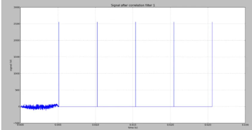
6.6 Graph received samples after correlation filter (bit sequence of 1023 bits) . 47 6.7 Auto-correlation for a 10-bit sequence . . . 47
6.8 Comparison between received signal and ideal signal . . . 48
C.5 Bode plot Htot(s) . . . 64
D.1 Testbench ADC . . . 66
D.2 Simulation ADC . . . 67
D.3 Testbench Ethernet . . . 68
D.4 Simulation sending Ethernet frames . . . 69
E.1 Rectified voltage(Yellow) and input current(green) . . . 71
E.2 Primary current(Yellow) and secondary current(green) . . . 71
E.3 Primary current(green) and rectified input voltage(Yellow) . . . 72
E.4 Primary current(Yellow) and secondary current(green) . . . 72
E.5 Voltage over the LED (Yellow) and current through the LED(green) . . . . 73
E.6 Voltage over the LED (Yellow) and current through the LED(green) . . . . 73
E.7 extra circuitry on breadboard . . . 75
E.8 Current through LED(Yellow) and voltage over the LED ( 17.8V to 30.7V)(green) . . . 75
E.9 Current through LED(Yellow) and signal from FPGA (green) . . . 76
E.10 Current through LED(Yellow) and signal at gate(green)) . . . 76
F.1 Graph received signal after correlation filter (6-register LFSR), one LED burning . . . 78
F.2 Graph received signal after correlation filter 1 (6-register LFSR ), 5 LEDs burning . . . 78
F.3 Graph received signal after correlation filter 2 (6-register LFSR ), 5 LEDs burning . . . 79
F.4 Graph received signal after correlation filter 3 (6-register LFSR ), 5 LEDs burning . . . 79
F.6 Graph received signal after correlation filter 2 (7-register LFSR ), 5 LEDs burning . . . 80 F.7 Graph received signal after correlation filter 3 (7-register LFSR ), 5 LEDs
burning . . . 81 F.8 Graph received signal after correlation filter 1 (8-register LFSR bit LFSR),
5 LEDs burning . . . 81 F.9 Graph received signal after correlation filter 2 (8-register LFSR ), 5 LEDs
burning . . . 82 F.10 Graph received signal after correlation filter 3 (8-register LFSR ), 5 LEDs
burning . . . 82 F.11 Graph received signal after correlation filter 1 (9-register LFSR ), 5 LEDs
burning . . . 83 F.12 Graph received signal after correlation filter 2 (9-register LFSR ), 5 LEDs
burning . . . 83 F.13 Graph received signal after correlation filter 3 (9-register LFSR ), 5 LEDs
burning . . . 84 F.14 Graph received signal after correlation filter (10-register LFSR ), one LED
burning . . . 85 F.15 Graph received signal after correlation filter 1 (10-register LFSR ), 5 LEDs
burning . . . 85 F.16 Graph received signal after correlation filter 2 (10-register LFSR ), 5 LEDs
burning . . . 86 F.17 Graph received signal after correlation filter 3 (10-register LFSR ), 5 LEDs
burning . . . 86 F.18 Graph received signal after correlation filter (11-register LFSR), one LED
burning . . . 87 F.19 Graph received signal after correlation filter (12-register LFSR), one LED
burning . . . 87 F.20 Graph received signal after correlation filter (13-register LFSR), one LED
burning . . . 88 F.21 Graph received signal after correlation filter (14-register LFSR), one LED
burning . . . 88 F.22 Graph received signal after correlation filter (15-register LFSR), one LED
burning . . . 89 G.1 Graph received signal after correlation filter (10-bit LFSR), one LED
burning . . . 91 G.2 Graph received signal after correlation filter (10-bit LFSR), 5 LEDs burning 91
H.8 Comparison output signal with different cut-off frequency of HPF . . . 105 H.9 PCB receiver with some modifications . . . 106 H.10 PCB sender schematic 2, with FPGA mounted . . . 108
2.1 Characteristics of BPW21R photodiode . . . 6
2.2 Characteristics of S1223 photodiode . . . 9
3.1 Comparative table between different switch uses . . . 17
6.1 Measurements radius versus correlation value with each LED . . . 49
ADC Analog-to-digital converter ARP Address Resolution Protocol ESR Equivalent Series Resistance FIFO First in, first out
FPGA Field-programmable gate array LED Light Emitting Diode
LFSR Linear Feedback Shift Register LSB Least Significant Bit
MII Media Independent Interface MSB Most Significant Bit
RAM Random Accessible Memory
THD Total Harmonic Distortion UDP User Datagram Protocol VLC Visible Light Communication
PD Photodiode
Introduction
LEDs are semiconductor devices that emit light when biased in the forward direction of the p-n junction. LEDs present many advantages over traditional light sources, including lower energy consumption, longer lifetime, improved robustness and smaller size. A significant attribute of LEDs is their ability to switch on and off thousands of times per second. No other lighting technology has this capability. This switching occurs at ultra-high speeds, so far beyond what the human eye can detect, that the light appears to be constantly on. These embedded signals are emitted from the LEDs in the form of binary code; ’off’ equals zero and ’on’ equals one. This is what they call visible light communication (VLC). When VLC equipment and devices are placed throughout a building of geographical area, a comprehensive wireless communication network can be created.
This thesis talks about a stand alone transmitter and a receiver that can be connected to a computer. The transmitter can be build in the ceiling and only needs 230 AC voltage to transmit digital information. The receiver will be a device to plug in a digital port of the computer. It receives information from the emitted light and send it to the PC. The transmitted information will give the receiver the possibility to determine his current position in a room by looking at the amplitude of the signals he receives from multiple LEDs. It can also be used to transmit other digital information/files.
Chapter 4 talks about the different parts of the receiver. First, we will tell how to supply the circuit. Afterwards, we will explain the receiver circuit starting from the photodiode until the ADC used to digitalize the analog signal.
In chapter 5 we have a look how the connection with the PC is made. This contains the VHDL code used to process the data from the receiver circuitry in the FPGA and send it to the PC. At the side of the PC, we use some software to obtain that information. The processing in software is explained in chapter 6.
The final result of our thesis is presented in chapter 7. The things we couldn’t do due to the time limit and the ideas we have in mind for future work are given in chapter 8.
Source code, schematics, calculations, documentation and extensive test results are found in the appendices.
Preparation and Research
2.1
Choice of emitting LED and receiving photodiode
2.1.1 Introduction
To start this project, we first had to look for the proper LED and photodiode that we would use. We need those specifications to know what spectrum we will use to transceive, what electrical circuit we need to control the LED and to process the received data through the photodiode.
2.1.2 LED
As we are researching an application for indoor use and we want to use LEDs to illuminate a room and to transmit data, we will work with white light. Two approaches are generally used to generate white light with LEDs. The first approach is to combine light from, e.g.,
Figure 2.1: Two approaches for generating white emission from LEDs.[11]
red, green and blue (RGB) LEDs [11]. Typically, these triplet devices consist of a single package with three emitters and combining optics, and they are often used in application where variable color emission is required. These devices are attractive for VLC as they
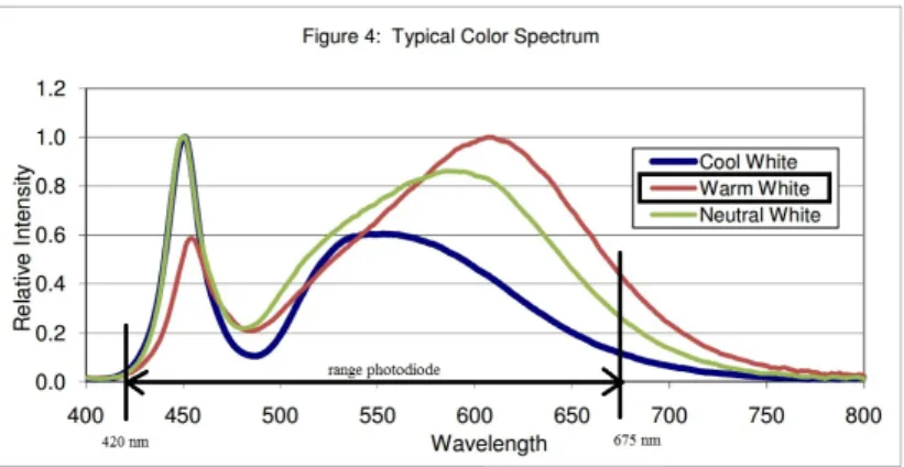
In the domain of white light you can choose 3 main types of white light LED’s : Cool, Warm and Natural White LEDs (see Figure 2.2)
Figure 2.2: Different kinds of white light.[9]
With traditional incandescent or halogen bulbs you could not choose the colour of the light that the bulb produced as this was down to pure physics. Traditional bulbs work by passing electricity through a wire that glows hot. This glow produces the light that can be seen. Because LED bulbs are a completely different technology and much more technically advanced it is possible to choose the colour of the light that you want.
The colour temperature of light can be measured as a number on the Kelvin scale. This is represented by a number followed by the symbol ’K’. High colour temperatures of over 5000 K are said to be cool colours and often have a blue tone to them. Whereas low colour
temperatures of 2,500 - 3,200 are said to be warm colours and have yellow or orangey tones to them.[13]
In domestic lighting, 75 - 80 % of customers buy warm white LED bulbs as they offer the closest match to their old incandescent or halogen bulbs that they are replacing. The light given off by a warm white LED bulb can be described as soft and warm with a slight yellow hint to it.
Some customers purchase cool white LED bulbs if they want the brightest light possible or if they want to achieve a modern look to a room. This particularly suits colour schemes that are bright and bold and use primary colours, or even colour schemes that are predominantly white where a clean minimal look is required.
In commercial lighting the majority of customers opt for cool white bulbs. These give a brighter light but you should be careful to ensure that the colour temperature is not too high, or in practical terms the light not too cool, otherwise the effect may seem very harsh or displeasing to the eye.
These 3 main different white LEDs have a different Intensity division in the spectral band.(See Figure 2.3)
Figure 2.3: Typical Color Spectrum.[3]
2.1.3 Photodiode
The first part of a VLC receiver, is a photosensitive element. Mostly, a photodiode is used at the input of the receiver. The current through the photodiode, is proportional to the light falling on it. The more light it receives, the larger the current will be.
Figure 2.4: Spectrum of warm-white LED in comparison with the range of the photodiode
Figure 2.5: Photodiode BPW21R
Hereby, We summarized the most important characteristics of the photodiode BPW21R in table 2.1:
Parameter Value Unit
Sensitive area 7.5 mm2
Short circuit current at 1 klux 9 µA
Sensitivity 9 nAlux
Wavelength of peak sensitivity 565 nm
Range of spectral bandwidth 420 to 675 nm
Viewing angle ± 50 ◦
Rise time 3.1 µs
Fall time 3.0 µs
Diode capacitance ifVR=0 V 1.2 nF
The photodiode has a large sensitive area, what is interesting to capture enough light from the LED. The current will increase pretty fast when more light is falling on the diode because of its high sensitivity. The highest sensitivity takes place on a wavelength of 565 nm, which is in the spectrum of the LED. The rise time and fall time of a photodiode is defined as the time for the signal to rise or fall from 10% to 90% or 90% to 10% of the final value respectively. The bandwidth of the photodiode can be estimated using the formula:
BW ≈ 0.35t
rise ≈
0.35
3.1 µs ≈ 112.9 kHz
The BPW21R has also a wide viewing angle, so it can pick up light from several directions. The capacitance of the diode can play an important role at higher frequencies.
In the figure below, you can see the graph of the short circuit current in function of the illuminance. As expected from a photodiode, the current is proportional to the incident light. An interesting thing to see, is that the photodiode has to be in short circuit for linear working.
The relative spectral sensitivity versus the wavelength is shown in figure 2.7. We see that the range of spectral bandwidth (where S(λ)rel= 0.5) goes from 420 nm to
675 nm, as already mentioned in the characteristics. They also show the spectral response of the human eye VλEye. The human eye is also a photosensitive element.
It is most sensitive at a wavelength of 560 nm. The BPW21R photodiode gives thus an approximation to the spectral response of the human eye.
Figure 2.6: Short Circuit Current vs. Illuminance
Figure 2.7: Relative Spectral Sensitivity vs. Wavelength
• The BPW21R photodiode is a good choice as a receiver for the visible light communication, but can give some problems at higher frequencies because of the limited bandwidth and the capacitance. So, we also searched for another photodiode to encounter these problems. We found the S1223 photodiode from Hamamatsu [6] (see figure 2.8).
Figure 2.8: Photodiode S1223
table 2.2:
Table 2.2: Characteristics of S1223 photodiode
Parameter Value Unit
Sensitive area 6.6 mm2
Short circuit current at 100 lux 6.3 µA
Sensitivity at 660 nm 0.45 WA
Wavelength of peak sensitivity 960 nm
Range of spectral bandwidth 320 to 1100 nm
Bandwidth 30 MHz
Diode capacitance ifVR=20 V 10 pF
If we compare these characteristics with the characteristics of the other photodiode, we can notice some things:
The range of spectral bandwidth is larger. The photodiode is also sensitive in the infrared region. The diode is most sensitive in this region, but he is also sensitive in the spectrum of the LED. So, we can also use this photodiode as a receiver because we will filter the ambient light. This photodiode is more appropriate at higher frequencies because of the higher bandwidth and the smaller capacitance. The rise time can now be estimated using the formula:
trise≈ 0.35BW ≈ 30 MHz0.35 ≈ 11.667 ns
In figure 2.9, you can see the spectral response of the photodiode. As already mentioned, the diode is most sensitive in the infrared region.
If we want to simulate a circuit with a photodiode in LT Spice, a photodiode is not available in the component library. So, we will use an equivalent model that represents the photodiode. First, we used a normal diode in parallel with a current
Figure 2.9: Sensitivity vs. Wavelength
source to model the photoelectric effect. The more light falling on the photodiode, the more current will flow through it. However, the results from the simulations and the measurements were not very similar. Then we modified the model by placing a capacitor in parallel with the diode and the current source. The capacitor represents the photodiode capacitance. You can find this value in the datasheet. Now the results were much better. Simulations and measurements were very similar. Eventually we can also add the dark resistance of the diode. But this is usually very high (≈ 30 GΩ), so this is not very necessary. Finally we used the model below in LT Spice to represent the photodiode.
Figure 2.10: Model of photodiode
2.1.4 Conclusion
Because of the lowcost, the lower complexity and since we will transmit data over the whole visible spectrum, we chose the blue led with yellow phosphor coating approach. Whereas we want to implement our application in daily life, we chose to work with warm
light. The warm light has the closest match to the old incandescent of halogen bulbs that they are replacing and it has more intensity around 565 nm. After a chat with Frederic Truffer who works in the light department of the HES-SO in Sion we decided to use the BXRA-30E0740-A-00 star array led. This BXRA reaches a Typical Pulsed Flux of 860 lm. This should be enough to be detect by the photodiode at a distance of several metres. The characteristics of the chosen LED are listed in figures 2.11 and 2.12.
We chose to work with the S1223 photodiode because of the high bandwidth and the small capacitance. We will transmit data at 200 secondkbits , so that the photodiode has enough time to respond to the incoming light. Because of the high sensitivity and the large sensitive area, the distance between the LED and the photodiode should be no problem. The photodiode has a sensitive range that lies in the wavelength spectrum of the LED. If we consider this, the S1223 photodiode should be an appropriate photodiode for the visible light communication.
Figure 2.11: Main characteristics of the BXRA-30E0740-A-00 [3]
control the current through the LED. On the market you can buy a readily available LED driver, for our led we could use the 3-Watt MagTech LED Driver L03U-350 (see Figure 3.1).
Figure 3.1: LED DRIVER
We could use this driver or make our own driver and use this together with a switch for our VLC application (see Figure 3.2).
Most drivers use Switch Mode Power Supply (SMPS) topologies where the output voltage or current is determined by the frequency at what a switch is turned on and off. We wonder if it is possible to use this switch instead of an extra switch after the AC/DC converter to send information in a VLC application and control the output current at the same time. So we will construct our own LED driver and control the current through the LED. At first we will investigate the possibilities of sending data by controlling the switch of a Switch Mode Power Supply with an FPGA. The use of a switch after the LED driver will also be
Figure 3.2: VLC Circuit
investigated.
3.2
Power Supply Topologies
There are a lot of Power Supply Topologies we could use for our application. We must use an Switch Mode Power Supply as we want to control the switch for sending our data. In general this method is more interesting in comparison with series-controlled regulators that don’t use a switch, looking at the power loss. A list with a short description of these SMPS topologies is given in appendix A.
We will use the flyback converter due to his low cost, simplicity of design, small size and intrinsic efficiency. Other advantages of the flyback transformer over circuits with similar topology include isolation between primary and secondary and the ability to provide multiple outputs.
3.3
Flyback Converter
A flyback converter is a transformer-isolated converter based on the basic buck boost topology. The basic schematic and switching waveforms are shown in Figure 3.3. In a flyback converter, a switch (Q1) is connected in series with the transformer (T1) primary.
The transformer is used to store the energy during the ON period of the switch, and provides isolation between the input voltage source VINand the output voltage VOU T. In a steady state
of operation, when the switch is ON for a period of TON, the dot end of the winding becomes
positive with respect to the non-dot end. During the TON period, the diode D1 becomes
reverse-biased and the transformer behaves as an inductor. The value of this inductor is equal to the transformer primary magnetizing inductance LM, and the stored magnetizing
energy from the input voltage source VIN.Ep=12· IPK2 · LM & IPK =
VIN· TON
LM
Therefore, the current in the primary transformer (magnetizing current IM) rises linearly
from its initial value I1to IPK, as shown in 3.3(D). As the diode D1becomes reverse-biased,
Figure 3.3: Flyback Converter Circuit[7]
value should be large enough to supply the load current for the time period TON, with
the maximum specified drop in the output voltage. At the end of the TON period, when
the switch is turned OFF, the transformer magnetizing current continues to flow in the same direction. The magnetizing current induces negative voltage in the dot end of the transformer winding with respect to non-dot end. The diode D1 becomes forward-biased
and clamps the transformer secondary voltage equal to the output voltage. The energy stored in the primary of the flyback transformer transfers to secondary through the flyback action. This stored energy provides energy to the load, and charges the output capacitor. Since the magnetizing current in the transformer cannot change instantaneously at the instant the switch is turned OFF, the primary current transfers to the secondary, and the amplitude of the secondary current will be the product of the primary current and the transformer turns ratio, NP/NS.
3.4
LFSR
To control the mosfet for sending signals with the LED we need a certain signal to be generated. We chose to use a semi-random generated signal. For this we use a shift register expanded with xor functions (this is an example of an LFSR).
3.4.1 First tests
For the first tests we chose to work with a 3-bit LFSR (figure 3.4). This LFSR generates a bit sequence of 0,0,1,0,1,1,0.
Figure 3.4: 3-bit LFSR
We can program this LFSR in an FPGA. We used an FPGA board available at school with a Spartan XC3S500E FPGA from Xilinx on it to do the testing.
3.4.2 Final LFSR
As will be explained in the further text, we will only need a semi-random LFSR to be generated by a FPGA we will mount on the board. To be able to detect these LFSRs, we will use correlation. Later on we will test the response for LFSRs with different lengths. We always use maximum feedback xor combinations to generate a binary sequence with a length of 2m−1bits, where m is the length of the used register. [8]1
3.5
LED Heatsink
When a voltage is applied across the junction of an LED, current flows through the junction generating light. It is a common misconception that LEDs don’t generate heat. While
1a list of tabs for maximal feedback can be found on http://www.newwaveinstruments.com/
Where:
Pd is the thermal power to be dissipated
Vf is the forward voltage of the device
If is the current flowing through the device
The power calculation should be made for maximum dissipated power, which is computed using the Maximum Vf at the drive current desired.
Heat generated at the LED junction must be transferred to the ambient via all elements that make up the thermal management solution. These elements include the LED Array, the thermal interface material used between the LED Array and heat sink, the heat sink, the luminaire enclosure (if applicable), and other components that come in contact with the lighting assembly. These elements transfer heat to the ambient. We will use a heat sink to manage the temperature at the case of the LED array. The calculation of the maximum needed thermal resistance of the heat sink is included in appendix B.
We chose to use the SA-LED-151E - HEATSINK, LED, 50.8MM of OHMIT which have a thermal resistance of 3.2◦C/W , which is way below the maximum of 11.85◦C/W . This heat sink should keep the LED junction on a temperature below 70.5◦Cand the casing on a temperature below 57.01◦C.
3.6
Testing circuit 1
For the first tests, we designed a transformer circuit (schematic included in annex H.1) where we implement a power switch chip for the start up cycle and also to do the first tests. With a switch we can turn of the function of the POWER switch and give the control of the flyback to the FPGA. For the feedback of the power switch we use an analog feedback circuit, for the feedback to the FPGA we can expand our PCB with a ADC to measure the current through the LED. By reading this current, the FPGA will interact by changing the duty cycle of the control signal for the transformer switch when needed.
3.6.1 Tests First test
For the first test, we only looked at the functionality of the transformer operating with the power switch chip. The block diagram is given in fig 3.5. The results are discussed in appendix E.1.
Figure 3.5: Block diagram 1
As seen in appendix E.1, a custom made transformer should be calculated to have a maximum efficiency and maximum luminance. Due to the restriction of time and great advantages (shown in table 3.1) of the topology when placing a switch in serie with a LED driver (see following sections) we will continue by using the topology where we place a switch after the flyback.
Table 3.1: Comparative table between different switch uses
Property using switch of flyback using switch in series with LED
Transformer custom made general transformer can be used
with tolerance in values
Design multiple feedbackloops needed,
change of flyback switch after startup, larger circuitry and more components
relatively simple design
Transmission frequency fixed and determined by transformer
can be chosen by the user
Second test
We choose to obtain the same circuitry, only using the power switch chip and placing a capacitor in parallel with the LED as load storage. A switch will be used to generate current pulses trough the LED. For this tests we use a external programmed FPGA (We place it on
Figure 3.6: Block diagram 2
As the results of the second test met our expectations, we designed a new circuitry that will be discussed in the next paragraph.
3.7
Testing circuit 2
For the new circuit, we will mount an FPGA on the board. We will use one FPGA to generate the binary sequences for all the different LEDs to obtain a lower cost and a synchronization of the different LEDs. We expect that the synchronisation of the LEDs will make it easier to distinguish the different bit sequences in the received signal. We used the Actel igloo AGL 060V5 -VOG100. Because of his PROM memory we don’t have to program it every time we power it. The Actel igloo don’t support complicated designs, what we don’t need as we just want to generate LFSRs. This FPGA was used in a previous project at HES-SO Valais/Wallis what makes it easier to implement it in our design. We used that previous design as a template for our application. We used only a part of testing circuit 1 and added the FPGA, a DC/DC converter(to power the FPGA), a mosfet (as switch in serie with the LED) and an extra storage capacitor for a normal working of the Flyback. The schematic is added in appendix H.3. We use one schematic for the PCBs with and without FPGA. All the components with *(snm) don’t have to be mounted on the PCBs without FPGA. The VHDL code and block diagrams used to program the FPGA can be found in section 3.7.3.
3.7.1 Twisted pair cable
To drive the MOSFETs of the different LED circuits, we need to transport a blockwave on different places in the room. To transport these signals we have to look how we can transport them without great distortion or noise. The simplest way to do this is to send through a twisted pair cable. We test the deformation of the signal on a twisted pair cable of 6 meter (largest distance of 2 LEDs in a room). The result is given in figure 3.7. We see a
ringing effect et the end of the cable. As this ringing only lasts for about 300 ns and our bit period is 5 µs, this signal is only used as switch and we already have noise and peaks in our transmitted light signal (which are not detected by the receiver). This result is sufficient. We will connect the output of the FPGA directly with the mosfets in series with the LED. If we would work on a higher frequency, we would have to take this ringing into account.
(a) signal transmitted at FPGA (green curve), signal at the end of the cable (yellow curve)
(b) signal transmitted at FPGA (green curve), signal at the end of the cable (yellow curve) (zoom in)
Figure 3.7: Result twisted pair cable (6m)
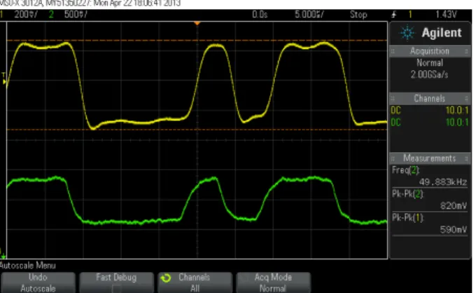
3.7.2 Tests
We regulate the potentiometer to get a current of maximum 500 mA through the LED and program the FPGA to generate LFSRs. In figure 3.8 you can see the current trough the LED in comparison with the signal sent by the FPGA. We can see that we have some ripple and spikes on the current signal. We won’t try to prevent this because this has no effect on the received signal by the receiver circuit. To regulate the LEDs on the same intensity we can look on the oscilloscope with a current probe. But we will check on every board by looking at VAU X (here 16.5 V). We checked and tested the resistance of the potentiometer and it was
each time around 15 kΩ.
3.7.3 VHDL of sender FPGA
As already mentioned we generate sequences with a FPGA. For each led we need a different LFSR (3.9a). The MSB of the LFSR is sent to the mosfet of each LED which get in conduction (1) or isolation(0) mode. When the MOSFET is in conduction mode, current flows through the LED and the LED emits light. When the MOSFET is in isolation mode, no current can go through the LED so the LED is not illuminating. For the readability of the code we wrote all the LFSRs in one block and used this for every LED. The correct LFSR is chosen by the number of the LED the block gets as a generic. The code can be found in appendix I.1.3.
Figure 3.8: Signal from on-board FPGA (yellow) and current trough LED (green)
We also did some tests in appendix G to send data over these LFSRs by just inverting the sequences. The block diagram is shown in figure 3.9b. The second clock represent a clock with a frequency of fclock
2n−1∗m where n is the length of the register of the LFSR and m is a
natural value. We did the tests by shifting a sequence and ’xor’ed this with the output we already had. The code is not included in this report because of its simplicity.
(a) LFSR sending sequence generation
(b) LFSR sending sequences generation with data.
The receiver circuit
4.1
Introduction
We already discussed the photodiode we will use for the visible light communication. As mentioned before, the short-circuit current through the photodiode is proportional to the incident light. If we want to know the bits that are transmitted, we have to use several blocks. First of all, we will use a current-voltage converter, so that the voltage is also proportional to the incoming light. We also need a high pass filter to filter out the ambient light and the 100 Hz frequency components coming from the lighting in the building. Since the signal we will receive is weak, we will have to use an amplifier. Then, we also need an ADC to digitalize the received signal. Before the ADC, an anti-aliasing filter is needed. Finally, the digital samples have to be transmitted to a PC so we can use software to make some calculations and to find the position. We will use an Ethernet cable for the connection. The block diagram of the receiver circuit is shown below. We will discuss the several blocks and the power supply as well in this chapter. The Ethernet connection and the data processing on the PC will each be discussed in a separate chapter.
Figure 4.1: Block diagram receiver
Figure 4.2: Step-up converter (1.2V to 3.3V)
We have to put some components around the MCP 1640 chip. The input capacitor of 4.7 µF is recommended to decouple the voltage source. For low power applications, this capacitance is sufficient at the input. We have to use an X5R ceramic capacitor with a low ESR. The inductor of 4.7 µH is an essential element for a step-up converter. It is a buffer for electrical energy and it is needed if we want a higher output voltage than the input voltage. To achieve a high efficiency, we also need an inductor with a low ESR. To calculate the values of the resistors (voltage divider), the datasheet gives the formula:
RT OP= RBOT T OM· (VVOU T
FB - 1)
If we want VOU T = 3.3 V, and with VFB= 1.21 V and RBOT T OM = 300 kΩ, we find: RT OP=
518.18 kΩ ≈ 510 kΩ.
The output capacitor of 10 µF ensures a stable output voltage during sudden load transients and reduces the voltage ripple. To have a low ripple, we need a condensator with a low ESR. Again, we can use an X5R ceramic capacitor.
The question is now whether this voltage is enough to supply the op-amps we will use in our circuitry. So, we first searched for the op-amps and see what supply they need. We chose the AD817AN op-amp (see further). This op-amp cannot be supplied with a single 3.3 volt. We supplied it with a single 5 volt. Another way to supply the circuit had to be used. We also found a step-up converter to boost 1.2 volt to 5 volt (see below). When we build the
circuit on a breadboard (with low ESR inductor and short connections), the circuit worked when there was no load. Once we connected the receiver, the voltage dropped to 3.5 volt what is not enough to supply our circuit. The step-up converter can’t deliver enough current for a proper working of the receiver circuit.
Figure 4.3: Step-up converter (1.2V to 5V)
Then we tried to feed our circuit with the 5 volt from the USB port. This power supply is inherently unstable and depends on the load of the computer. Normally the supply can vary between 4.75 and 5.25 volt. But it can also be possible that the voltage drops to 4.4 volt or even lower. When we tried this to power our circuit, it worked. This 5 volt is used to supply the op-amps. This supply is not so critical, so our circuit will also work properly even if we don’t have a stable supply voltage.
4.3
Current-voltage converter
To convert the current from the photodiode in a voltage, we have to use a current-voltage converter. A common way to do this, is to use an op-amp for it, as shown in figure 4.4. In an ideal op-amp the voltage on the minus pin is the same as the voltage on the plus pin. So, the photodiode is in short circuit. If we look to the graph of the short circuit current vs. illuminance (see figure 6.5), we see that the current is proportional to the incoming light if the photodiode is in short circuit.
To have an idea about the current through the photodiode and the voltage after the I-V converter, we set up the circuit of figure 4.4 (with R1 = 100 kΩ, an LM324 op-amp and
the BPW21R photodiode) on a breadboard and did some measurements. To determine the current, we can measure the voltage across the resistor. First, we looked what the voltage was in the office with infalling sunlight and with a fluorescent lamp at about two metres from the photodiode (VR1,light). Then, we looked what the voltage was when no light was
falling on the diode, VR1,no−light. We found:
Figure 4.4: Current-voltage converter
VR1,no−light ≈ 5 mV
The current through the photodiode is (almost) equal to the current through R1:
Ilight = 100 kΩ0.3V = 3 µA
Ino−light= 100 kΩ5 mV = 50 nA
The output voltage VO= - VR1.
VR1,light ≈ -0.3 V
VR1,no−light ≈ -5 mV
4.4
Ambient light filter
The photodiode will also pick up ambient light and light coming from the lighting in the building. Those have to be filtered out. The lighting in the building are fed from the net of 230 VRMS at 50 Hz. Due to the rectification, there will be radiation of 100 Hz frequency
components that can influence the working of the photodiode. So, we need a high pass filter with a cut-off frequency fcut−off above 100 Hz to filter the ambient light and the
components of 100 Hz. Our first thought was to build a simple RC high pass filter (see figure 4.5) after the current-voltage converter. [2]
The formula for fcut−offis then as follows:
Figure 4.5: RC high pass filter
If we take fcut−off=200 Hz and R=100 Ω, then we find: C=7,9577 µF. We take the standard
value C=10 µF.
The cut-off frequency becomes: fcut−off=159,155 Hz. This value is good to filter the
unwanted light.
If we make the circuit, the results are very poor. The bandwidth of the photodiode is large enough for the 100 kHz signal, so the problem must be something else. The characteristics of the LM324 op-amp aren’t good enough for a square wave of 100 kHz. Two important characteristics of an op-amp are the bandwidth and the slew-rate. We found for the LM324 op-amp:
• Bandwidth: 1 MHz • Slew rate: 0.4 V
µs
If we use another op-amp (AD817AN), the results are better: • Bandwidth: 50 MHz
• Slew rate: 350 V µs
In first instance, the op-amp is supplied with ± 15 volt. If we switch the LED on and off at 100 kHz, we get a signal at the output of the receiver as you can see in figure 4.6.
We can see that the DC component is filtered out, but there is oscillation at the transition from low to high, so the circuit is not ideal to filter the ambient light.
Another thought for the filtering was to put a capacitor (10 nF) between the photodiode and the minus pin of the op-amp as you can see in figure 4.7.
Now we get a signal like you can see in figure 4.8.
The signal is better, but we can still see some high frequency components in the signal. The original rectangular shape is not so good visible anymore, the edges are flattened.
Figure 4.6: Output receiver with RC-filter
Figure 4.7: Ambient light filter circuit with capacitor
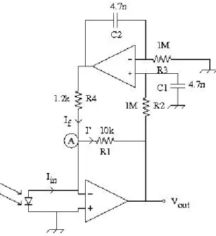
came to the circuit of figure 4.9. We use a feedback circuit that cancels out frequency components below a certain frequency. You can find more explanation about the circuit and the calculation of the transfer function and the cut-off frequency in appendix C.
Until now, we always supplied the op-amps with ± 15 volt. We need three connectors to provide this supply. It should be easier to work with a single supply so we just need two connectors. Since we want to make a portable device, we will use lower voltages. The AD817AN op-amp needs at least a 5 volt single supply, so we will use this voltage to feed the op-amps.
Figure 4.8: Output receiver with condensator
Figure 4.9: Receiver circuit
By using a single positive supply, negative voltages cannot be generated. We will use a virtual ground instead of the normal ground. This special ground is usually a voltage reference half way between 0 volt and the supply voltage. In our case, the virtual ground will be 2.5 volt and can be made with a voltage divider and a voltage follower as shown in figure 4.10. [10]
Figure 4.10: Creating a virtual ground for single supply operation
from dual to single supply operation, we have to replace the normal ground by the virtual ground.
4.5
Amplifier
Since the signal is too weak after filtering, we will use an amplifier. The amplification is needed if we want to use the full range of the ADC. After some measurements, we took an inverting op-amp with a gain of 100. Before the amplifier we put a high pass filter with fcut−o f f = 2·π·5100·10·101 −9 = 31.2 Hz and a gain of 1. We did this because we still had an
offset after the ambient light rejection circuit. We also tried to use two op-amp stages with each a gain of 10, but the results weren’t so good. We still had an offset and there was more noise in the signal. So, we decided to use a high pass filter with a gain of 1 and an inverting amplifier with a gain of 100.
When we simulated the ambient light rejection circuit, no offset was visible. We just had a DC offset of 2.5 volt because we are working with a virtual ground.
We also tried to build a high pass filter with a gain of 100, but an offset was still visible.
4.6
Anti-aliasing filter
It is recommended to use a low pass filter before the ADC to prevent aliasing. The Nyquist theorem says that the sample rate must be minimum twice the highest frequency component in the analog signal, if we want to reconstruct it properly. As we want to sample at 1 MHz, we will use a filter with a cut-off frequency of maximum 500 kHz.
The easiest and most common way to make a low pass is just to use a simple RC filter. In this case, it’s not a good idea. RC filters are cheap, but at higher frequencies LC filters are a better choice. LC filters don’t make use of resistors, so they don’t dissipate power (in the ideal situation). We want a high order low pass filter with a steep attenuation curve to prevent aliasing. We chose to work with a 7th order filter (4 inductors and 3 capacitors) to have enough attenuation at 1 MHz. A 7th order filter has an attenuation of 7 · 20 decdB =
140 decdB. To calculate the values of the components, we used the program RFSim99 at the recommendation of Mr Rieder M´edard. In this program we can calculate and simulate the filter we need. We have to give the filter type (Butterworth or Chebyshev), the cut-off frequency, the order of the filter and the input and output impedance. We chose for a 7th order Butterworth filter with a cut-off frequency of 500 kHz and an input and output impedance of 50 Ω. In the beginning, we chose this impedance because the spectrum can be easily measured with a network analyzer (optimized for input and output impedance of 50 Ω). Later on, we replaced the input and output impedance with these of our circuit and looked how the spectrum of the filter changed. Once we have the calculated values, we took the nearest standard values. Finally, we had a result as you can see in figure 4.11.
Figure 4.11: LC filter with fcut−o f f = 500 kHz and Zin= Zout = 50 Ω
With the help of Mr Rieder M´edard, we built the filter (figure 4.12) and measured the frequency spectrum of the filter with a network analyzer. The result can you see in figure 4.13. We can see that the filter is ideal to prevent anti-aliasing. We have a cut-off frequency (3 dB attenuation) of 474 kHz and at 1 MHz (sample rate), we have an attenuation of 36 dB.
Figure 4.12: LC filter with fcut−o f f = 500 kHz and Zin= Zout = 50 Ω (PCB)
The problem is that the output and input impedance of the filter is supposed to be 50 Ω. In our circuit, this is not the case. The question is how the filter will react if we deviate from
Figure 4.13: Spectrum LC filter measured with network analyzer (50 Ω input and output impedance)
these impedances. The input impedance in our circuit is low (≈ 1 Ω), because the filter comes after an op-amp stage. The output impedance is determined by the voltage divider to buffer the ADC and is about 300 Ω. We simulated the filter with LT Spice with those impedances and had a look at the frequency spectrum (figure 4.14). We can see that there are some peaks above 0 dB in the spectrum which can cause oscillation. Nevertheless, we built the filter on a PCB to see what it gives. To built a good filter, it is also important to use inductors and capacitors with a low ESR so the losses are as low as possible.
Figure 4.14: Simulation spectrum LC filter with Zin= 1 Ω and Zout = 300 Ω
the signal before and after the filter (after the voltage divider). First, we switched the light on and off on the rhythm of a 100 kHz square wave at a distance between the LED and the receiver of 2,3 m. The results are shown in the picture below. The green curve represents the signal before the filter and the yellow curve after the filter. As you can see, the high frequency components and the noise are filtered out. The square wave has become almost a sine wave.
Figure 4.15: Signal before and after filter at 2,3 m (square wave)
If we want to see for oscillation, we drive the LED with a 3-bit LFSR as discussed in chapter 3. Now we can see some oscillation in the signal. If the signal goes from low to high or vice versa, an overshoot occurs. As this is not very desirable, we tried to rebuilt the filter.
Figure 4.16: Signal before and after filter at 2,3 m (LFSR)
Again, the RFSim99 program was used. Now we tried to build a filter with Zin= Zout= 300
Ω and afterwards we adapted the input and output impedance to respectively 1 Ω and 300 Ω and simulated it in LT Spice. Now we have a spectrum as shown below. The characteristics
Figure 4.17: Simulation spectrum LC filter with Zin= 1 Ω and Zout= 300 Ω (redesign)
We changed the filter on the PCB and looked at the signal when we drive the LED with an LFSR. We can see that the high frequency components are filtered and there is almost no oscillation. We will use this filter in our circuit.
Figure 4.18: Signal before and after filter at 2,3 m (LFSR) with new LC filter
4.7
ADC
If we want to send the information to a computer, we need to digitalize the data. We chose to work with a 12-bit resolution ADC. With 12 bits, we can get 212= 4096 possible digital values at the output of the ADC. If we supply it with 3.3 volt, the input range goes then from 0 volt to 3.3 volt. If we supply it with 5 volt, the input range goes then from 0 volt to 5
volt. As the FPGA is also supplied with 3.3 volt, the ADC also has to be supplied with this voltage, because we are sending data from the ADC to the FPGA. The FPGA doesn’t accept signals with an amplitude of 5 volt. So, we have a resolution of23.3V12−1 = 805.86 µV. We need
a high resolution if we want to accurately measure the amplitude of the input signal. The ADC consists of a successive approximation register with internal track-and-hold. The conversion rate is determined from the serial clock (SCLK) and can be up to 1 MSPS. The timing diagram for the ADC can you see in the figure below.
Figure 4.19: Timing diagram 12-bit ADC
A conversion process begins on the falling edge of CS. This process takes 16 periods of SCLK. On the first three falling edges of SCLK, a zero is transmitted. After this, the 12 data bits are clocked out on the rythm of SCLK, beginning with the MSB of the digital value. When the process is done, CS is brought back high and the output returns in tri-state. CSmust stay high during tQU IET before a new conversion process can begin.
We drived the ADC by programming an FPGA so the signals CS and SCLK are properly sent like shown in the timing diagram. We chose to work with fSCLK = 22 MHz and tQU IET
= 22 MHz6 = 272.727 ns. For one sample we need 16 periods of SCLK for the conversion and 6 periods of SCLK when CS is high. In this case, we have a sample rate of 16+622 = 1 MSPS. The datasheet mentions that fSCLK should be maximum 20 MHz. But thus we tried it with
22 MHz and it also worked. If we drive the ADC, we have a serial output as shown below. The upper signal is the CS signal, the signal below is the serial output. In appendix I, you can find the code we used to program the FPGA. The simulation of the ADC can also be found in annex D.1.
We used an FPGA board (see figure below) available at school with a Spartan XC3S500E FPGA from Xilinx on it to generate the signals CS and SCLK.
The board has to be supplied with a single 5 volt. On the right side, there are two 26-pin connectors so we can connect the FPGA with another circuit. We used this connector to exchange data between the receiver and the FPGA. There are also some possibilities to
Figure 4.20: Signals CS and SDATA
connect the board to a PC. There is an RS232 port, an Ethernet port and a USB port. The schematic of the board and the UCF file can be found at the Wikipedia website of HES-SO Valais/Wallis 2. We will also use this board for the connection to the PC. This will be explained in the next chapter.
Figure 4.21: FPGA board
Every ADC contributes to the increase of noise at the input, the so-called sampling noise. The datasheet mentioned that the ADC will deliver best performance when driven by a low-impedance source. The voltage divider before the ADC (and after the filter) has to be done with low resistances. We chose the values 51 Ω and 240 Ω so that we have the full range (0 → 3.3 volt) at the input of the ADC at small distances between the LED and the receiver (less than 50 centimeters). The input of the ADC sees the 240 Ω of the voltage
divider (see the schematic of the receiver in appendix H.2) in parallel with some other resistances. But the 240 Ω will determine the source impedance of the ADC. If we look to the graph T HD vs. Source impedance (see figure 4.22), 240 Ω should be low enough to prevent distortion.
Figure 4.22: THD (dB) vs. Source impedance (Ω)
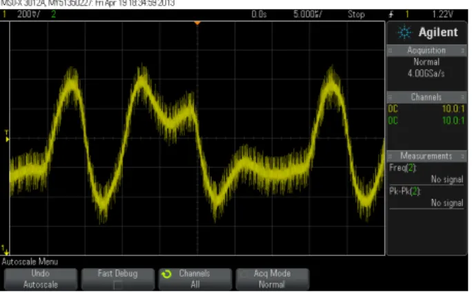
The datasheet also says that the sampling will cause input current pulses that result in voltage spikes at the input. Every time that the ADC goes from track mode to hold mode or vice versa (see figure 4.19), a spike will occur. When we drive the ADC, we see the signal below at the input.
Figure 4.23: Input signal ADC when driven by FPGA (LFSR at 2,3m)
Figure 4.24: Input signal ADC when driven by FPGA measured with probe with ground wire.
As the signal seen on the oscilloscope is maybe not the real signal (because of the capacitance of the probe), we want to send the data to a computer and plot it in a software program such as Matlab, Octave or Python. Another thing we are interested in, is the influence of the spikes for the sampling value.
The final schematic of the receiver (from the photodiode to the ADC) is added in appendix H.2. The circuit on PCB is shown in the picture below.
Connection to the PC
5.1
Introduction
As we have now the data from the ADC, we want to visualize it on the computer to see how the sampled signal looks like. To make the connection, we have several possibilities: RS232, USB, Ethernet, ... Since we are clocking out the data at a frequency of 22 MHz, the link we will using should be fast enough.
RS232 is intended for data rates up to 20 kbps. So, this is too slow for our application. USB 2.0 can be used for speeds up to 480 Mbps.
Ethernet can reach speeds up to 100 Mbps.
Since the driving of the Ethernet port is already available in VHDL at HES-SO Valais/Wallis, we chose to work with Ethernet for the FPGA-PC communication. If we want to send data on an Ethernet link, we have to encapsulate it with a header. This packet is called an Ethernet frame. In the header, you can find the MAC address of the sender and the receiver, the IP address of sender and receiver, a CRC,... The data should be at least 46 bytes and maximum 1500 bytes.
5.2
Structure Ethernet communication
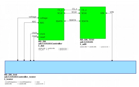
The structure to send and receive Ethernet packets with the samples of the ADC included, can be seen in figure 5.1. The block on the right represents the ADC. We get an analog input value, this is converted into serial data (SDATA) with the signals SCLK and CSn. In
the U DP Application block, we find the ADC controller that converts the serial data into parallel data. The parallel data is stored in RAM and put in a frame at certain moments (explanation see further). In this block, we decide the destination UDP port, IP address and MAC address. If we want to send a frame, the data and some information for the header (UDP port, IP address, MAC address) is given to the U DP Fi f o block. The data is processed via a FIFO structure. This block gives the data to the MII to RAM block that is an interface between the U DP Fi f o block and the Ethernet controller on the FPGA board (or
Figure 5.1: Structure to send and receive packets over Ethernet
We don’t have to change the U DP Fi f o block and the MII to RAM block. In our case, we just have to adapt the U DP Application block that determines which data we put in RAM and when we want to send a new frame.
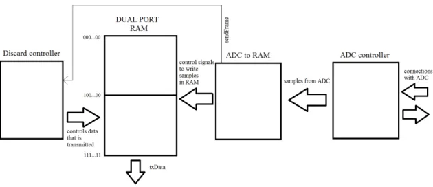
To write the samples from the ADC in the Dual Port RAM and to send them in a frame, we used the structure as shown in figure 5.2.
The ADC controller drives the ADC and gets the serial data that represents the taken samples. To put the samples in RAM, we used an interface between the ADC controller and the RAM: ADCtoRAM. This block writes the samples in RAM. When CSnbecomes high,
a new sample is available. To put the 12-bit samples easily in RAM, we added four zeros before each sample so we have 16 bits (two bytes). Because the RAM is byte addressable, it’s easier to work with 16 bits than with 12 bits. The signal writeEnA is high during two clock periods. During the first clock period, the eight MSB’s of the sample are stored in RAM. During the second clock period, the eight LSB’s are stored in RAM. The signal addressAis incremented once we have stored a new byte. If half of the RAM is stored with new samples, the signal sendFrame is brought to 01 for one clock period. If sendFrame = 01, the first half of the RAM is read and sent via txData. While reading from the RAM, we can keep on writing in the other half of the RAM. If sendFrame = 10, the second half of the RAM is transmitted. Meanwhile we can keep on writing in the first half of the RAM. The code we used for the different blocks can be found in appendix I.1.2. Once we had written the code, we could program the FPGA and make the connection to the PC with an Ethernet cable. There are two types of Ethernet cables: a straight through Ethernet cable and a crossover Ethernet cable. Normally we should need a crossover Ethernet cable to
Figure 5.2: Structure to write the samples in RAM and read from RAM
make the connection between the FPGA and the PC. But the Ethernet controller on the FPGA board can automatically detect which cable we are using. So no distinction should be made. We chose to work with a straight through cable because they are more common. If there is data transport over the cable, we can see two status LEDs blink. The left LED is constantly on and is a speed indicator. If this LED is on, it means that we have a 100 Mbps connection. The other LED blinks if there is some activity on the cable. We used a CAT 5e Ethernet cable which is fast enough for the 100 Mbps data transport.
Now we have connection with the PC, we can see the received packets in Wireshark as shown in figure 5.3. We can see the IP address given by the FPGA (169.254.111.1). The destination IP address is put to 0.0.0.0, because the FPGA doesn’t know our IP address yet. We first have to send a frame to the FPGA, so he can store our IP and MAC address. We put 1024 data bytes (512 samples) in one packet and every second we received almost 2000 packets. Now we can see the packets in Wireshark, we can use software to process the data.
Figure 5.3: Received UDP packets in Wireshark
The construction of the receiver and the Ethernet connection to the PC is shown in figure 5.4. The receiver circuit is connected with the FPGA board. The FPGA drives the ADC on the PCB and sends UDP packets to the Ethernet connector. When a connection with the PC is established, we can see the LEDs blinking on the connector. The supply for the receiver circuit and the FPGA board is done with a USB cable.
send and receive UDP packets. There is a library socket that we can import in the program. Before receiving the samples, we first have to send a UDP packet to the FPGA so he can store the IP address and MAC address of the PC. As we have several interfaces (network adapters) on the computer, we first have to bind the socket to the interface we want. In the Commandwindow, we can see the several interfaces and their IP addresses (see figure 6.1) via the command arp -a. As we want to use the Ethernet adapter, we bind to IP address 169.254.227.40. Once we bind to the socket, we can send data to the FPGA and we can choose a UDP port. The Python code we used to send a UDP packet to the FPGA, can be found in appendix I.2.1. Later on, we put this code in a function and we call it in the main program. The structure of our code is explained in the next paragraph.
Figure 6.1: Network adapters on PC
Firstly, we didn’t see the packet in Wireshark so no packet was sent to the FPGA. When we looked in the ARP table of the Ethernet interface, the IP address and MAC address of
the FPGA couldn’t be seen. So, we added manually the IP address and MAC address of the FPGA to the ARP table via the command: arp -s 169.254.111.1 e4-af-a1-39-02-01. This operation needs administrator rights. If we now look to the ARP table (see figure 6.2), we can see that the addresses are added.
Figure 6.2: ARP table
If you look at figure 6.3 you can see the packet in Wireshark, so the packet is sent to the FPGA. If the FPGA receives the UDP packet properly, the destination IP and MAC address in the FPGA are changed to those of the PC as we can see in Wireshark. When the FPGA receives a UDP packet, a LED on the FPGA board is blinking.
Now we can send a packet to the FPGA, we can start receiving the ADC samples.
We bind the socket to UDP port 9 because the frames are send to this port. We can receive packets from all IP addresses who send a packet to port 9. The processing of the received samples is explained in the next paragraph.
Figure 6.3: Sending a UDP packet to FPGA
6.2
Processing the data
To make the code more readable, we chose to work with a main script where we call the functions we want to implement. The functions are defined in a separate file and can be imported by the main.
The block diagram of the main is shown below.
Figure 6.4: Block diagram of the main code
The main script starts with sending a UDP packet so the FPGA knows our IP address and MAC address. Then, we calculate the bit sequences sent by the LEDs. These bit sequences are used to filter the received data.
Because the time between the samples of the ADC is 1 µs (1 MHz1 ) and the time between the bits in the sequences is 5 µs, we get 5 samples for 1 bit. We repeat each bit in the generated sequence 5 times to match the generated and the received sequences. If we have for instance the bit sequence 0 1 1, we used a function to make 00000 11111 11111.
We can also determine in the main on how many packets we want to do the calculations. In one packet, 1024 bytes (512 samples) are included. As we have 5 samples per bit, we have
about 100 bits in one packet. This is not enough if we send a long bit sequence.
In appendix F, we tested several bit sequences: going from a 6-register LFSR sequence (26 - 1 = 63 bits) till a 15-register LFSR sequence (215- 1 = 32767). The results are discussed in the appendix. For the indoor positioning, we chose to work with a 10-register LFSR sequence (210- 1 = 1023). Now, we can start receiving the data. Every time a new packet arrives, we put the 1024 data bytes in a bytearray. To make it easier to do calculations, we convert the bytearray in a list of integers. Since we want to have the value of the samples (which are two bytes), we calculate the samples and store them in a list of 512 elements. If we have for instance 06 FF, we can calculate the sample via 255 + 6 · 162= 1791. Now we have calculated the samples, we can also calculate the corresponding analog values as seen on the oscilloscope with the formula : maximum valuevalue sample · 3.3 volt = value sample4095 (FFF) · 3.3 volt. In our example we find: 17914095 · 3.3 volt = 1.44 volt. If we want to represent the samples in a graph, we have to determine what the time is between two successive samples. This is given by the sample frequency: 1 MHz. So, the time between two samples is 1 MHz1 = 1 µs. As we could still see some spikes in the graph, we wrote a function to reduce the peaks. In the graph below, you can see the sampled data from one packet (512 samples). The largest peaks are filtered out.
Figure 6.5: Graph received samples (bit sequence of 1023 bits)
Afterwards, we used the function lfilter to filter the received signal with each of the bit sequences sent by the LEDs. The function y = lfilter(b,a,x) requires three arguments. brepresents the array representation of the nominator coefficients of the filter. a represents the array representation of the denominator coefficients. x represents the input array that we want to filter. In the Z domain, we can write y in function of x:
Y(z) = b0+b1·z−1+···
a0+a1·z−1+··· · X(z)