Active Pixel Sensors for X-ray Astronomy
by
Matthew Cohen
Submitted to the Department of Electrical Engineering and Computer
Science
in partial fulfillment of the requirements for the degree of
Master of Science
at the
MASSACHUSETTS INSTITUTE OF TECHNOLOGY
Aug 2005
®
Massachusetts Institute of Technology 2005. All rights reserved.
Signature'redacted
A uthor
.
..... . . . ..-..
. . .
. . . .
. . .
Department of Electrical Engineering and Computer Science
Signature redacted
August,11,2005
Certified by .
...
.
'
..
...
Mark W. Bautz
Principal Research Scientist
Sig nature redacted
Thesis Supervisor
C ertified by ....
...
Kent H. Lundberg
Post-Doctoral Lecturer
>Thesis S>ipervisor
Signature redacted
A ccepted by ...
.
.. .
.
.
. . . . .
Arthur C. Smith
Chairman, Department Committee on Graduate Students
MASSACHUSETTS INSM UTE
ARCHNES
OF TECHNOLOGY
Active Pixel Sensors for X-ray Astronomy
by
Matthew Cohen
Submitted to the Department of Electrical Engineering and Computer Science on August,30 2005, in partial fulfillment of the
requirements for the degree of Master of Science
Abstract
An active pixel sensor array, APS-1, has been fabricated for the purpose of scientific x-ray detection. This thesis presents the results of testing the device. Alternate design architectures are explored. Recommendations are made for a next-generation sensor.
CCDs have been the dominant x-ray sensor in astronomy for over ten years. Lim-itations inherent to CCDs are starting to become important. Active pixel sensors
(APS) provide an alternate architecture that may solve these problems.
APS-1 is a first-generation sensor designed by Lincoln Laboratory's Advanced
Sil-icon Technology Group. APS-1 is fabricated in a fully depleted silSil-icon-on-insulator
(FDSOI) technology. FDSOI is especially well-suited to produce a scientific x-ray
im-ager. The device includes sixteen different pixel variations to determine the processing parameters that can produce the best imager. Dark current, noise, and responsivity of the various pixel designs was measured using an electronics system adapted from a CCD test system. X-rays were detected at room temperature.
Ordinary active pixels have high noise levels (~ 70 electrons). Many pixel designs
capable of lower noise have been presented in the literature. Active reset, pixel-level
CDS, and CTIA pixel designs are discussed in detail and simulated.
A second-generation sensor from Lincoln Laboratory, using pixel-level CDS, is
discussed. This device, APS-2, will be available for testing in 2006. APS-2 simulation results are presented. It is expected to have an input-referred noise of less than five electrons, near the performance of modern CCDs.
Thesis Supervisor: Mark W. Bautz Title: Principal Research Scientist Thesis Supervisor: Kent H. Lundberg Title: Post-Doctoral Lecturer
Acknowledgments
First I have to thank my supervisor Mark Bautz for the extremely generous support (both financial and academic) he has given me during the last year and a half. Mark has always been available to discuss this project, even when in Japan. When this thesis took longer than originally planned, Mark kept me on payroll for a few extra months. He took an electrical engineer who knew nearly nothing about astrophysics as a student, and for that I am forever grateful.
I also must thank my co-supervisor Kent Lundberg. Dr. Lundberg took me on as a thesis advisee relatively recently, when I discovered that I needed to have a co-supervisor. He, more than anyone, is responsible for this being a complete thesis. Dr. Lundberg kept pushing me to get more accomplished, even when I didn't seem to be listening. He has devoted a significant amount of time to this project even though it is not related to his research. Thanks for sticking with me.
Although they are not official co-supervisors, this thesis would not have happened without the help of Vyshi Suntharalingam at Lincoln and Steve Kissel and Gregory Prigozhin at MIT. Despite her incredibly hectic schedule, Vyshi took time to meet with me weekly, giving tons of pointers on what to do and how to do it. Steve knows the XIS electronics and all of its quirks, and was invaluable in the lab. Gregory has always been here with helpful suggestions and answers to all my questions, as well as plenty of questions that steered this project in the right direction.
Thanks to Dick Elder for all his assistance with the electronics design. Thanks to Rick Foster for his suggestions regarding the test system. Much thanks to Fred Miller for quickly removing and resoldering components for me, and never complaining about it. Thanks to Beverly Lamarr for always being around to help with any computer issues that I had. Thanks to Eric Austin at Lincoln for all his help with testing the devices, both in the clean room and via email. Thanks to Peter Csatorday for always being there to suggest a particularly interesting NY Times or cnn.com article to read
as a distraction from my work.
We celebrated my 'graduation' over two months ago, and now I'm actually finishing. Thanks for encouraging (i.e. nagging) me to get my work done.
I also need to thank my wonderful girlfriend Emily for sticking with me during
these last few months. I first met Emily as this project was really getting underway. Originally, she thought this would be done by early May. Then mid-June. Finally it's August, and the thesis is actually finished, and I can spend some time with her
again. She's been incredibly supportive and I couldn't have done this without her. Well, there you have it. To paraphrase Wayne Campbell.. .I hope you find this thesis whimsical, yet relevant, with an underlying revisionist conceit that belies the
thesis's emotional attachments to the subject matter. Party on!
This work was supported by the National Aeronautics and Space Administration
(NASA) through grant NAG-5401 to the Massachusetts Institute of Technology and through NASA Defense Purchase Request (NDPR) S-06566-G.
This work was sponsored by the United States Air Force under contract
#FA8721-05-C-0002. Opinions, interpretations, conclusions, and recommendations are those of
Contents
1 Motivation: From CCD to APS 11
1.1 T he C C D . . . . . 11
1.2 The Active Pixel Sensor (APS) ... 14
2 First Generation sensor: APS-1 17 2.1 Process Overview . . . . 17 2.2 Im ager D esign . . . . 19 2.2.1 Pixel variations . . . . 20 2.2.2 Output Circuitry . . . . 25 2.3 Sum m ary . . . . 28 3 Test Setup 29 3.1 Astro-E2 XIS Overview . . . . 29
3.1.1 Controller Board . . . . 30
3.1.2 Driver Board . . . . 31
3.1.3 Video Board . . . . 33
3.2 APS-1 and XIS Electronics . . . . 34
3.2.1 APS-1 Requirements . . . . 34
3.2.2 XIS M odifications . . . . 35
3.2.3 Pixel Readout Sequence . . . . 40
3.3 Sum m ary . . . . 41
4.1 X-ray Sensitivity and Responsivity 4.1.1 Experimental Setup . . . . 4.1.2 Results . . . . 4.1.3 Conclusions . . . . 4.2 Dark Current . . . . 4.2.1 Experimental Setup . . . . 4.2.2 Results . . . . 4.3 N oise . . . . 4.3.1 Experimental Setup . . . . 4.3.2 Results. . . . . 4.4 Summary . . . .
5 Review of Pixel Designs
5.1 Standard Reset Methods . . . . .
5.1.1 Hard Reset . . . .
5.1.2 Soft Reset . . . .
5.2 Combining hard and soft reset . .
5.2.1 Pseudo-flash reset . . . . .
5.2.2 Flushed reset . . . .
5.2.3 Hard-to-soft reset . . . . .
5.3 Active Reset . . . .
5.3.1 Fowler active reset pixel
5.3.2 Pain active reset pixel
5.4 Capacitive Manipulation . . . . .
5.4.1 Kleinfelder CDS pixel. . .
5.4.2 Takayanagi feedback pixel
5.4.3 Capacitive Transimpedance
5.5 Summary . . . .
Amplifier
6 Detailed Pixel Analysis
6.1 Signal-Chain Noise ... 43 44 46 49 51 51 52 58 59 59 60 63 63 64 65 66 66 67 68 68 68 69 70 70 71 72 73 75 75
6.2 Active Reset Pixel . . . .
6.2.1 Tim ing . . . .
6.2.2 Analysis and Noise Modeling . . . .
6.3 Kleinfelder CDS Pixel . . . . 6.3.1 Tim ing . . . .
6.3.2 Analysis and Noise Modeling . . . .
6.4 CTIA Pixel . . . .
6.4.1 Fixed Pattern Noise . . . .
6.4.2 Timing and Gain Selection . . . . . 6.4.3 Analysis and Noise Modeling . . . .
6.5 Simulation . . . .
6.5.1 Standard APS Pixel . . . .
6.5.2 Active Reset Pixel . . . .
6.5.3 Kleinfelder CDS Pixel . . . . 6.5.4 CTIA Pixel . . . . 6.5.5 Simulation Summary . . . . 7 The 7.1 7.2 7.3 7.4 Future: APS-2 Process overview Imager design 7.2.1 Layout Simulation . . . . Conclusions . . .
8 Conclusions and Future Work
8.1 APS-1 Testing . . . .
8.2 Pixel Designs . . . .
8.3 Summary . . . .
A Transient Noise Analysis Tool Verification
103 103 103 104 105 107 109 109 110 111 113 77 78 80 83 83 84 85 85 87 88 89 90 91 94 97 99
B APS Users Guide
B.1 Typical Current Draw ...
B.2 Starting EGSE ... ...
B.3 Turning System Off ... B.4 Dummy Load ... ...
B.5 Single pixel scoping ... B.6 Single pixel digital readout ...
B.7 Subarray digital readout ...
B.8 Single pixel signal current analysis . . . . B.9 Multiple pixel photocurrent analysis-short integration times B.10 Multiple pixel photocurrent analysis-long integration times
C APS Test System Reference
C.1 Background Documentation
C.2 DAC Channel Assignments.
C.3 Sequencer Operation . . . . C.4 .com files . . . . C.5 .sdoc files . . . . C.6 Shell Scripts . . . . C.7 IDL routines . . . . C.8 Probe Card . . . . C.9 Dummy Load . . . . C.10 XIS to APS Conversion List
C.10.1 Driver Board . . . .
C.10.2 Video Board . . . . . C.10.3 Controller Board . .
C.10.4 Address Latch Board
C.10. 5 C.10.6 129 . . . . 12 9 . . . . 1 2 9 . . . . 13 1 . . . . 1 3 1 . . . . 13 5 . . . . 13 6 . . . . 13 8 . . . . 139 140 140 140 142 143 144 146 146 Board-to-board Jumper Wires
Cables . . . . 115 115 116 117 118 119 121 122 124 126 127
Chapter 1
Motivation: From CCD to APS
Since the launch of the ASCA mission in 1993, the detector of choice in x-ray
as-tronomy has been the charge-coupled device (CCD) [1]. CCDs offer very low-noise
performance and high quantum efficiency, with well-understood radiation-tolerance characteristics. CCDs are a mature technology, and they are the reason behind the great success of the Chandra X-ray Observatory, Hubble Space Telescope, and other ground- and space-based astronomical observatories.
Nevertheless, CCDs are far from ideal. The effects of radiation damage are known all too well: the CCDs aboard Chandra were damaged by radiation encountered just after launch, resulting in increased dark current and decreased spectral resolution. Other limitations inherent in the CCD architecture include long readout times, the need for thick optical blocking filters, and the inability to integrate signal processing circuitry on the same die as the CCDs [2]. A new technology, active pixel sensors
(APS), potentially offers solutions to all of these problems.
1.1
The CCD
Invented in 1969, the CCD was originally intended as a memory element [3]. The
CCD is essentially an analog shift register: charge packets are pumped across the CCD
in response to changing voltages on a series of electrodes. By placing photosensitive elements throughout the device, the CCD can be used as an image sensor, its primary
Figure 1-1: A four phase CCD. As the electrodes are pulsed in sequence, charge packets are shifted down the line (shown here in vertical succession) [4]
application today.
Modern CCDs are composed of side-by-side MOS capacitors. A four-phase CCD is shown in Figure 1-1. Each clock phase is individually pulsed, creating high- and low-potential regions in the substrate, resulting in charge being dumped from beneath one electrode to the next. Once the charges reach the end of the row, they go through another shift register, until the data from each pixel in each row has been shifted out of one output node. CCDs are operated using correlated double sampling to reduce noise. Scientific CCDs have low enough noise that they are capable of measuring the quantity of charge generated by an incident x-ray, with an error of only a few electrons, RMS, allowing the x-ray photon energy to be determined very precisely.
The most recent x-ray CCD mission, Astro-E2 [5, 6], uses CCDs with 1026 rows and 1024 columns, with a 24 pm pixel pitch, and four parallel output nodes. Noise is less than 2.5 electrons RMS at a readout rate of 41 kpix/sec. Both front-illuminated and back-illuminated CCDs are present on Astro-E2. The front-illuminated de-vices have depletion regions of 60-65 [um, as compared with 40-45 pam on the back-illuminated ones. The back-back-illuminated devices collect photons in the range 0.3-10 keV; front-illuminated devices have a lower limit of 0.6 keV. The CCDs have excellent spectral response, exhibiting a full-width half-maximum of approximately 130 eV for incident photons at 5.9 keV; the level of the spectral peak is 45 times its width [1, 7]. Although extremely high performance CCDs exist, the limitations of the devices
are becoming apparent. In a CCD like the one in Figure 1-1, each packet of charge must be transferred four times per pixel*; consequently, CCDs must have a very high charge transfer efficiency (CTE), the percentage of charge to be successfully transferred per phase. CTE must typically have a minimum of at least five nines
(0.99999) [4]. To achieve such high CTE, the clocking voltages must be precisely
controlled both in time and magnitude, with voltages on the order of 15 V typical of scientific devices [8].
Since only one pixel can be read at a given time, the time to read the whole CCD is typically several seconds. Long readout times can lead to loss of data through pileup, where two x-ray photons strike a pixel before readout can be completed. There is consequently a maximum x-ray intensity that can be observed with a CCD, with brighter sources causing frequent pileup.
X-ray CCDs are sensitive to IR, visible, and UV radiation also. Although these lower energy photons create much smaller charge packets than x-rays (typically one electron per photon [9]), accumulating charge from too many out-of-band photons in an exposure leads to loss of precision in measuring x-rays. To prevent this data corruption, large, fragile filters are used to block out-of-band radiation. The heavy shielding used to prevent contamination also reduces the amount of soft (low energy) x-rays reaching the detector. Soft x-rays are important scientifically, so it is unde-sirable to lose this data. If the readout speed could be increased, the required filter would be much smaller, and less likely to interfere with soft x-rays.
CCD fabrication processes are generally not capable of producing CMOS
electron-ics, which means that all signal processing must be done off chip, on dedicated circuit boards. These boards add greatly to the power consumption and mass of space-based telescopes. An ideal detector would incorporate CMOS analog and digital processing on the same die as the detectors.
*Modern CCDs use three phases, reducing charge transfers by 25%. Charge packets may still be transferred thousands of times.
VRST VRST
RSTG- VDD RSTGH . VDD
PG TX
M.M W 3
ROW RTW
(a) Photodiode (b) Photogate
Figure 1-2: Standard three-transistor APS pixels. Pixels consist of photodetector, reset transistor, source follower, and row-select switch. After the reset transistor turns
off, charge integrates on the photodetector. The source follower acts as a buffer, and
the row-select switch is used to choose which pixel to read out. The photodetector may be (a) a photodiode or (b) a photogate.
1.2
The Active Pixel Sensor (APS)
One recent challenger to the CCD is the active pixel sensor (APS). The active pixel sensor is descended from the original MOS image sensors, which, like the CCD, were invented in the late 1960s [101. The original MOS sensors were passive pixel sensors. Each passive pixel contained a photodiode and an access transistor. At the bottom of each column was an integrating amplifier.
Passive pixel sensors were plagued with problems, including high noise, slow read-out, and lack of scalability. The solution was to add an amplifier within each pixel. This new device is the active pixel sensor. The APS pixel solves the noise, speed, and scalability issues of the passive pixel sensor [4, 10]. APS imagers still suffer from higher fixed pattern noise than CCDs, but active pixel sensors are catching up with respect to noise, dynamic range, and responsivity [101.
The standard CMOS active pixel consists of three transistors and a photodetector (Figure 1-2). The photodetector is typically a photodiode or photogate. The reset transistor, M,,t, pulls the detector back up to a high voltage after readout. Signal is buffered through a source follower, M ,, with Mei serving as a row-select switch, allowing the pixel to be multiplexed onto a column bus.
One major advantage of APS imagers are that they can be fabricated in standard
as the sensors. Single-chip cameras that incorporate sensors, processing, and A/D conversion have been produced [8].
Many other advantages exist when astronomy is considered as a primary applica-tion. Charge packets do not need to be transferred across the whole array, but rather across a single pixel. Since the integrity of the charge packet is most vulnerable to radiation during transfer [2], APS imagers are much less vulnerable to radiation. It is also possible to read out each column simultaneously, creating much shorter readout times. As described earlier, quicker readout reduces pileup and out-of-band contami-nation, along with other benefits such as less noise due to dark current, and possibly higher operating temperature. Due to fast readout, an APS telescope will not need a blocking filter, greatly improving its reliability and ability to detect soft x-rays. Since it is CMOS-based, an APS imager does not need tightly controlled, high voltages, like a CCD does.
Although it is very promising, APS is still an immature technology. Commercial
CMOS processes do not produce active pixel sensors suitable for ray detection;
x-ray imagers have different requirements than visible ones. Thick depletion regions are needed to efficiently absorb x-rays. Dynamic range is typically important for visible imagers, while the dynamic range of a typical x-ray sensor is on the order of 70 mV. Noise is one of the most important metrics for scientific sensors. Commercial APS devices typically have read noise on the order of 50 electrons; much lower noise is necessary for a device to have scientific value.
This thesis is the beginning of attempts to surmount the difficulties involved in creating an x-ray active pixel sensor. Chapter 2 discusses a first-generation APS im-ager designed and fabricated at Lincoln Laboratory. Chapter 3 presents a system
I designed to test this device. Results of testing are presented in Chapter 4.
Var-ious advanced pixel designs are explored in Chapters 5 and 6. Chapter 7 discusses a second-generation APS imager designed at Lincoln Laboratory. Conclusions and recommendations for future work are presented in Chapter 8.
Chapter 2
First Generation sensor: APS-1
Lincoln Laboratory's Advanced Silicon Technology Group has designed and fabricated a first generation x-ray active pixel sensor. This device, known as APS-1, is described in this chapter.
2.1
Process Overview
APS-1 was fabricated in a 0.35 pm, 3.3V fully depleted "Imaging/Silicon-on-Insulator" (I/SOI) process [11]. The I/SOI process is optimized for low-voltage CCDs with
in-tegrated, on-chip CMOS devices. APS-1 is an experimental design to determine the quality of active pixel sensor that could be fabricated using this process.
SOI transistors are fabricated in a thin silicon layer atop a buried layer of silicon
dioxide. Beneath the oxide layer is the handle wafer, a thick layer of silicon which provides mechanical support. Each device is fabricated in its own island of silicon. The resulting isolation between each transistor results in lower parasitic capacitances and higher radiation tolerance as compared to bulk CMOS [12]. In SOI, transistors of opposite polarities can be very close without risk of latchup, whereas bulk CMOS devices must be far apart. Figure 2-1 illustrates some of the advantages of SOI over
bulk designs.
SOI processes are typically classified as either partially depleted (PDSOI) or fully depleted (FDSOI), depending on the thickness of the transistor layer. The more
Fully Depleted
S01
CMOS
n-Well Bulk CMOS
r~ 466 nm Fild
50 nm Si 200 nm Buried Oxidef\
High Resistivity Silicon Handle Wafer
Figure 2-1: A comparison of SOI and bulk CMOS processes. The figure on the left shows two SOI transistors, the 50nm BOX region, and the handle wafer. The figure on the right shows two bulk CMOS devices. In SOI, substrate coupling is minimal due to the thick oxide, while bulk devices have a small depletion region for isolation. In SOI, transistors of different polarities be tightly packed due to the absence of field oxide and lack of wells. In bulk CMOS, n-type and p-type devices must be kept far apart to avoid latchup. Image courtesy of Lincoln Laboratory.
common variety is PDSOI; because of the thicker layer of silicon (typically greater
than 0.15 pm [13]), a portion of the channel is not depleted. The result is a parasitic
BJT with a floating base in parallel with the SOI MOSFET. This BJT manifests itself
through the floating-body effect, which causes leakage currents, threshold changes, hysteresis, and other problems.
FDSOI processes offer several improvements over PDSOI. Since the entire
chan-nel (typically less than 0.10 Mim thick [13]) is depleted, the floating body effect is greatly reduced. Parasitic capacitances are smaller. Second-order effects such as short-channel and narrow-channel effects decrease, subthreshold slope is improved, and transconductance is larger. However, FDSOI transistors tend to have worse threshold voltage matching due to the dependence on the channel thickness [12].
Lincoln Laboratory's I/SOI is an FDSOI process. The I/SOI process differs from ordinary FDSOI processes in that it uses the thick handle wafer as a photosensitive region. Since the photodetector is located in a different layer than the readout elec-tronics, fill factor can be kept high despite the addition of more transistors per pixel. The buried oxide layer provides important isolation between the photodetectors and other nodes of the circuit.
Another benefit of the SOI nature of this process lies in the size of the detector
VRST VRST
RSTG-I MrSt VD- RSTGH rst VDD
Nt PG TX
ROW- -ROW ROW-I ROW
(a) Photodiode (b) Photogate
Figure 2-2: APS-1 four-transistor pixels. Pixels consist of photodetector, reset tran-sistor, source follower, and row-select switch. After the reset transistor turns off, charge integrates on the photodetector. The source follower acts as a buffer. The complementary row-select switch is used to choose which pixel to read out. The photodetector may be (a) a photodiode or (b) a photogate.
depletion regions [2]. Photodetectors in bulk APS devices have depletion regions less than 1 pm thick. In order to efficiently detect x-rays, much larger depletion regions are needed. Modern x-ray CCDs have depletion regions on the order of 50 pm. It is possible to obtain depletion depths of this magnitude in the I/SOI photodetectors by biasing the handle wafer properly, greatly improving quantum efficiency.
2.2
Imager Design
APS-1 is a 256x256 pixel array. Pixel pitch is 12 pm. The APS-1 pixel is similar to
the standard APS pixel (Figure 1-2), except that the row-select transistor is replaced
by a CMOS transmission gate (see Figure 2-2). The absence of well isolation allows
transistors of both polarities to fit easily within a single pixel, resulting in improved performance. In bulk APS devices, extra transistors in each pixel are avoided since they hurt fill factor. SOI devices can potentially be back-illuminated, with nearly
100% fill-factor. Although APS-1 is front-illuminated, the extra transistor was
in-cluded due to the potential for back-illumination.
Photodiode pixel -- -
-VRST VOD 4.8&.7 annuar
RSTG VDD VDD
4.&10.5 annular:
W ROW -hROW These current mirrors
*0 go to the same pad with
* 311 3A), I the same diode
--- -a -ad -connected transistors
m Pad Pad Photogate pixel ---. VRST _DD ICMIP I 4.50.7 annuar-RSTG -,",4 VDD ' an u C o lun R e a d o u t --- -PG TX C-6 CL Pad ROW -ROWpF SHR ^REF DD
h.a giat pm V).0 i.rh.. a nua- g. S ZF
V 55SIG
CCO -; - CCL Pad
+60 1Z C O 54pF
Pad SHS
Clocked input bias
Variable DC input bias
---Figure 2-3: Simplified schematic of APS-1. 4-T pixels are shown in upper left. Delta-difference sampling is implemented on a column level, with parallel readout chains for signal and reference levels. Also shown are some connections to pads for external current source biasing. Image courtesy of Lincoln Laboratory.
2.2.1
Pixel variations
The imager is a 256 x 256 array, divided into 16 subarrays (Figure 2-4), each of which differs in doping, geometry, or photodetector type (see Table 2.1).
Photodetectors
APS-1 pixels use two different types of photodetectors. PD1-PD12 use photodiodes,
while PG13-PG16 use photogates.
The simpler of the photodetectors is the photodiode (Figure 1-2(a)). Photons incident on the photodiode generate photocurrent. The reverse-biased diode acts as a capacitor, storing the generated charges. The voltage on the capacitor is the input to
cC) 0 cc LO a: C14 256 x 256 pixel array 16 blocks of 64 x 64 12pm x 12 pm pixel PD-1 PD-2 PD-3 PD-4 PD-5 PD-6 PD-7 PD-8 PD-9 PD-10 PD-11 PD-12 PG-13 PG-14 PG-15 PG-16
Signal and Reference S/H Vg 256 Column Decoder
Figure 2-4: APS-1 is divided into 16 subarrays, each 64x64 pixels.
the source follower. The end result is that light on the photodiode causes the voltage at the pixel output to fall.
After a suitable exposure length, or integration period, the output voltage is sam-pled. Transistor Mrst is then turned on, resetting the pixel. Typically, a sample is taken immediately after reset also, for use in a double sampling scheme such as delta-difference sampling [14], where the two voltage levels will be subtracted later in the readout chain. Note that in this scheme the signal and reset levels are from two different exposures. They are therefore uncorrelated, and this subtraction will not eliminate reset noise. The only way to do a true correlated double sampling would be to store a whole frame of data on chip, which is impractical.
The operation of a photodiode APS pixel is shown in Figure 2-5 as three separate scope traces. In darkness, with the exception of a pulse due to the diode being reset, the waveform is nearly flat. With low light incident on the pixel, the output voltage drops over time. Bright light causes the voltage to reach a saturation point before it can be reset.
Detector Type BCCF SCP Bulk SOICS SOI-CMOS TX Gate
Iimplant Implant LOCOS implant Gate Shape Length
PD-1 PD Straight PD-2 PD Y Straight PD-3 PD Y Straight PD-4 PD Y Straight PD-5 PD Y Straight PD-6 PD Y Y Straight PD-7 PD Y Y Straight PD-8 PD Y Y Straight PD-9 PD Y Annular PD-10 PD Y Y Annular PD-11 PD Y Y Annular PD-12 PD Y Y Annular PG-13 PG Y Annular 1.0-1.3 prm PG-14 PG Y Annular 0.5-1.35 prm PG-15 PG Annular 1.0-1.3 pm PG-16 PG Annular
0.5-1.35
prmTable 2.1: Pixel variations in APS-1. Pixels differ in implant types, geometries, photodetector types, and transistor sizes.
Photogates are an alternative to photodiodes. In these devices, charge integrates in a deep potential well underneath a photogate. Separating the accumulating charge from the output node is the transfer gate, typically biased near VDD/2. While the voltage on the photogate is high, integrated charge will remain beneath the photogate. Pulsing this voltage low dumps the charge across the transfer gate, onto the floating output node, which is the input to the source follower. Each pixel is essentially a miniature CCD, with very short charge transfer distances [81.
Photogates have several advantages over photodiodes. The equivalent capacitance of a photogate can be much smaller than that of a photodiode. Reset noise, the main noise source in an active pixel sensor, is proportional to the square root of this capacitance. Consequently, photogates are typically less noisy than a photodiode, without any other changes to the readout circuitry.
More significantly, it is possible to do true CDS with a photogate. The problem with using CDS with a photodiode is that it is necessary to store the reset level for every pixel in the array, and there is no way to include a full frame buffer and still maintain a high fill factor. The photogate, with its separate integration node and readout node, provides exactly this sort of structure. Using CDS completely
M20,09S A .f 1.22Vf M2O.OI.$ A 1.60 V M20.OJ9S A f 1.22V4.
& 3'S2900Oi ____ _ A4ROOps -33.29Op
(a) Photodiode in darkness (b) Photodiode in low light (c) Photodiode in bright light
Figure 2-5: Oscilloscope traces of the output waveform from photodiodes. (a) Pho-todiode in darkness. It is periodically reset, but the waveform is otherwise nearly flat. (b) Pixel under low light. The incident photons create a current that causes the output voltage to decrease. (c) Pixel in bright light. The photodiode's output saturates.
eliminates reset noise.
The main problem with photogates is their larger size. The photogate and transfer gate are both essentially transistors, meaning that the photogate pixel has nearly twice the size of a photodiode pixel, reducing fill factor. Additionally, not all process technologies are capable of producing photogates.
Implants and LOCOS
PD2, PD6, and PD10 pixels contain a buried channel/charge funnel (BCCF) implant in the active region of the diode in an attempt to minimize surface-state effects.
BCCF is a phosphorus implant with an energy of 125 keV, a dose of 1.25 x 1012 cm-2
,
and a tilt of 10 degrees.
PD3, PD7, and PD11 use a scupper (SCP) implant. The SCP implant is similar
to the BCCF implant, but at a much higher dose: it is a phosphorus implant at an energy of 150 keV, a dose of 1.0 x 1014 cm~2, and a tilt of 10 degrees.
PD4, PD8, and PD12 have extra regions of local oxidation of silicon (LOCOS). The LOCOS regions are in the bulk, above the diode region (see Figure 2-6).
All pixel types from PD5-PG14 contain an extra SOI channel stop (SOICS)
im-plant. The SOICS implant consists of 100 keV boron, with a dose of 5.0 x 10¹²
cm-2, at a tilt of 10 degrees. It is implanted underneath the SOI transistors to try to minimize dark current from the BOX/handle wafer interface.
(a) Pixel without LOCOS
Figure 2-6: (a) SEM of PD1. The gates of the four transistors are visible. (b) SEM of PD4, using LOCOS. The lighter gray regions in the bulk are the extra oxidation.
Geometry
PD1-PD8 use straight-gate transistors, while PD9-PD12 use annular-gate devices. The differences are illustrated in Figure 2-7. Conventional MOSFETs use straight gates. The gate polysilicon is a straight line dividing the diffusion region into a source and drain. The polysilicon overlaps the edges of the diffusion to ensure that the source and drain are not shorted. However, different characteristics at the diffusion sidewall cause this edge region to act as a parallel FET with a lower threshold voltage. The result is that straight-gate devices have high leakage currents. Annular gates are one attempt to solve this problem [15]. In annular-gate transistors the polysilicon gate creates a donut-shaped, or annular, division between source and drain. One terminal is entirely surrounded by poly and then by the other transistor terminal. The parasitic FET at the diffusion sidewall is now shorted out; its source and drain regions are at the same potential. Annular transistors should have much lower leakage currents than straight-gate devices. PD9-PD12 use annular transistors for the reset transistor and the source follower. Annular transistors occupy a slightly larger area than conventional ones.
(a) Pixel with straight gates
Figure 2-7: (a) SEM of PD1. The gates of all four transistors in each pixel are straight. These transistors are prone to leakage along the edges of the diffusion. (b)
SEM of PD9. The gates of the reset transistor and the source follower are annular.
The region where the gate overlaps the diffusion border is shorted since both sides of the parasitic FET are at the same potential, resulting in less leakage.
2.2.2
Output Circuitry
Delta-difference sampling [14] is implemented on the column-level. This sampling strategy entails parallel chains for reading out a signal level (pre-reset) and a refer-ence level (post-reset). The row-select switches within each pixel multiplex that row onto the column circuitry. Separate sample-and-hold switches for the signal (SHS) and reference (SHR) levels capture the appropriate voltages onto CSIG and CREF re-spectively. Each pixel in the selected row is then multiplexed onto the single set of output pads via the column select switches COL and COL. Normally the two output levels would be subtracted externally.
An additional feature in the column circuitry is the crowbar switch CB. After Vig and Vf have been read out, it is possible (though not necessary) to pulse the crowbar high, briefly shorting the two sampling capacitors. Ideally, the resulting levels on each would be midway between the signal and reset levels. However, threshold variations and other mismatches between the two chains result in a non-zero difference voltage even after the crowbar is pulsed. The new difference voltage may be subtracted from the original difference voltage, resulting in lower fixed pattern noise.
MMEMENOMMEMEWWWw EMN
Note that Voi9 and Vref are sampled onto two different capacitors. True CDS
requires that a single sampling capacitor be used. In addition, photodiodes operate in read-then-reset mode, so the sampled reset level will actually be the reset level for the subsequent integration. Since it is impossible to store that voltage on chip throughout the integration, however, there is no way to do CDS with photodiodes.
Crowbar Analysis
It is instructive to see how the crowbar reduces fixed pattern noise. Refer to Figure
2-3 for the schematic. The signal chain contains three source followers, only one of
which is guaranteed to match for the signal and reset samples (the in-pixel source follower is the same for both). Let the gains of these source followers be A1, A2, and
A3 for the signal path, and A4, A5, and A6 for the reset path. Let the input-referred
signal voltage be V, and the input-referred reset voltage be V. The output voltages are given by
Vsi, = AA2A3 Vs (2.1)
and
Vref = A4A5A6Vr. (2.2)
Without crowbarring, the input seen by the video electronics (assuming a differential first stage) would be the difference between these,
Vin = Vsig Vref = A1 (A2A3V9 - A5A6Vr) (2.3)
making use of the fact that A1 = A4. Crowbarring connects the inputs of the second
source followers together. Charge is split between the two capacitors CSIG and CREF,
so that the new capacitor voltages are given by
VCSIG VCREF = A-
(VCSIG
+ VrCREF)(2.4)
CSIG + CREFThe output voltages produced by charge sharing are given by
Vsig = A2A3 A1
(VsCSIG
+ VrCREF)(2.5)
CSIG + CREF
and
A 1 (VsCSIG + VrCREF)
CSIG + CREF
These are the crowbarred voltages, which are used as inputs to the same differential stage used for the original levels. The resultant difference signal is subtracted from the original difference signal. The input to the video electronics is therefore
Vn=
A,
[AAV-A
5AoVr
-(A 2A3 (VsCSIG + VrCREF) AAVCSIG
+ VrCREFCSIG + CREF CSIG + CREF
(2.7)
The goal is a signal directly proportional to Vig - Vrf. To realize this goal, first make the simplifying assumption that the capacitors are not mismatched, i.e. CSIG
CREF-Equation 2.7 then simplifies to
n=
AVA
2A
3Vs
_ A2A3Vr+ A5A6Vs A5A6Vr (28)VXK
A
1yA
2A
3V -AA
6V,
2-+
2+
.2).8
2 2 2 2
Gathering terms with V, and V gives the final result,
(A2A3
A
5A6(A
5A6 A2A3)Vin =A1
V\
2 + 2 Vr 2 + 2 AjA2A AA
= Al( 3 + A 26)(V, Vr). (2.9)
As desired, the input to the video board amplifier is proportional to V - V, with the gain given by
Gain = A1 (A2A 3 + AA6 . (2.10)
This gain is equal to the average gains of the individual signal and reset chains. If the capacitors CSIG and CREF are not precisely matched, there will be some mismatch-related errors, but this is a secondary effect, as integrated capacitors can be matched quite well.
2.3
Summary
APS-1 is an active pixel sensor imager optimized for x-ray detection. As the I/SOI
process is new, 16 different pixel variations were included in the array in order to determine what creates the best sensor. Extensive testing will reveal how each change influences the performance of APS-1.
Chapter 3
Test Setup
The Lincoln Laboratory-fabricated device APS-1 was tested using a modified ver-sion of the electronics from the Astro-E2 x-ray telescope. This chapter provides an overview of the Astro-E2 electronics as well as the modifications that allow these electronics to operate APS-1.
3.1
Astro-E2 XIS Overview
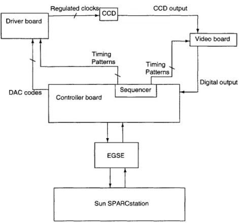
Much work has been done by the MIT CCD lab staff in preparation for the launch of the fifth Japanese x-ray astronomy satellite, known as Astro-E2 [6]. Astro-E2 contains, as one of its instruments, the X-ray Imaging Spectrometer (XIS) [5]. A team from MIT designed the analog electronics and CCDs for XIS. These electronics have become the standard CCD test platform in the lab, and as such it was desirable to attempt to run 1 using the XIS system. Adapting the XIS electronics for APS-1 necessitated substantial modifications to the electronics. The XIS system consists of three circuit boards: controller, driver, and video. The box containing these boards is connected to a Sun SPARCstation equipped with a DSP card, and an additional box (electrical ground support equipment, or EGSE) to simulate the interface with the rest of the spacecraft. Figure 3-1 is a block diagram of the XIS electronics.
Driver board
DAC codes
Regulated clocks ,= CODC CCD output
Video board Timing Patterns Timing Patterns Digital output Sequencer Controller board EGSE Sun SPARCstation
Figure 3-1: Block diagram of the XIS electronics. The controller board issues com-mands and timing information throughout the system. The driver board provides tightly regulated clocking and DC voltages to the CCD. The video board reads the
CCD and performs A/D conversion, sending the data back to the controller and
eventually back to the user.
3.1.1
Controller Board
The controller board is responsible for interfacing with the SPARCstation. Com-mands are received from the workstation and sent over the backplane to other boards in the system. The controller board is home to two other important systems: the housekeeping (HK) and sequencer.
Housekeeping
The HK system allows the XIS operator to monitor voltages and temperatures in the system, which would be otherwise impossible for an in-flight spacecraft. All important voltages on all the boards are multiplexed onto the HK bus on the backplane. When
the controller board receives a request for a particular measurement, the MUXes are set appropriately and the correct signal is routed to the controller, where a 16-bit
A/D converter captures the value and sends it back to the Sun.
Sequencer
From the point of view of the operator, the most interesting part of the controller board is the sequencer. The sequencer is used to provide precise control over CCD timing through the use of 16 control lines, called S-lines. The sequencer is connected to two small memories, known as the PRAM and SRAM. The PRAM stores a program for the sequencer to execute. The PRAM instruction set is quite small, limited to
loops, jumps, and three variations of SRAM reads. The SRAM contains the actual
waveforms for the S-lines.
Each SRAM location contains 48 bits of timing for each of the 16 lines. A typical example is shown in Figure 3-2. This figure comes from an actual data file used to program the SRAM. Note that the timing patterns for each of the control lines are given by a simple binary choice, which translates to 0 or 5 volts at the output of the sequencer. The sequencer runs on a 1,966,080 Hz clock, resulting in each timing bit lasting 508 ns, or one pixel minor cycle. A pixel cycle is composed of 48 pixel minor cycles. Each SRAM location stores one pixel cycle, or 24.384 ps, worth of data.
The simple variety of sequencer read command, SEQ, simply reads one pixel cycle worth of data and outputs it to the S-lines, while blocking any external commands received. The second variety, SEQE, is identical to SEQ but allows processing of any external commands received. The third form, SEQI, allows the user to specify an additional system-level command, typically a DAC change to occur at the same time.
3.1.2
Driver Board
The main purpose of the XIS driver board is to provide precisely regulated voltages for the clock* waveforms required by the CCD. The CCD is essentially an analog
*In this context clock does not necessarily refer to a strict periodic square-wave clock, but rather any waveform consisting solely of high and low levels.
time: 000000000011111111112222222222333333333344444444 012345678901234567890123456789012345678901234567 bO S1.OR Driver ... -bl S2.OR Driver .... ---b2 S3.OR Driver ----.-.---. -b3 -VINT- Video --- -b4 -VINT+ Video --- - - ---b5 -VTRACK Video ---- ... b6 VRST Video .... b7 (unused) Dri. .r.-.-.-b9 S2.IA Driver ---- ---- --
-blO S3.IA Driver
b11 S1.FS Driver . . . . . . . . .
b12 S2.FS Driver
b13 S3 .FS Driver - - - - - - - -
-b14 SRG Driver --- ---
---b15 (unused) ... ... .
Figure 3-2: Sample SRAM input for a CCD. The timing patterns for each of the 16 S-lines are clearly illustrated using dashes and dots. Each SRAM entry contains 48 timing bits for each of the 16 lines.
shift register, and as such its performance is very dependent on having the correct voltages applied. To that end, the driver board contains 16 8-bit DACs. In some
cases, two or three are actually used together to create bipolar signals. While the actual DAC outputs range from 0 to 2.5 V, amplification boosts the outputs to a typical range of approximately 0 to 13 V. The amplified, buffered DACs are known as the regulated DAC outputs, or just regulated outputs. Regulation circuitry for different DAC channels can vary widely depending on the needs of that particular signal.
The S-lines from the controller board arrive at the driver board via the backplane. On the driver board the clocks are used as the control inputs to analog switches. The switches select between different regulated voltages (determined by the DACs), sending these voltages to the CCD inputs. This arrangement of switches and DACs allows the sequencer, with its digital outputs consisting of either 0 or 5 V, to control a digital signal that may vary from -2 V to +13 V. The analog levels and timing patterns are separately programmable, allowing them to be fine-tuned independently of each other.
As a safety measure, the driver board power supply is partitioned into several local supplies, each of which has its own current limit set. If a current limit is exceeded, a switch is flipped, lowering the power supplies to a safe level. The only way to clear
current limiting is through a system reset. Limits range from 6 mA up to 97 mA.
3.1.3
Video Board
Capture, processing, and packaging of data from the CCD is done by the video board. Figure 3-3 is a block diagram of the video board analog electronics. Once per pixel cycle the video board initiates an A/D conversion. The video board contains four bit A/D converters (each XIS CCD contains four output nodes). A programmable 16-bit bias may be subtracted from the data immediately after A/D conversion, and this bias may be different for different A/D channels. Bias subtraction is useful because the whole 16-bit word is not sent back to the SPARCstation. Instead, the two least significant bits are always removed, and the user then has a choice of receiving the upper 12 or lower 12 remaining bits. If a sample appears to be out of range when operating in the low-range mode, it may be possible to save the data by performing the subtraction while still in 16-bit form. The truncation from 16 bits is due to the fact that XIS is intended to be operated in space. Bandwidth and power are limited,
and on the XIS the two LSBs do not provide useful data.
Since the CCD operates in a CDS mode, the video board needs to subtract two samples before A/D conversion. The subtraction is accomplished by combining cur-rent steering and an integrator. When the reset level is being read out, a curcur-rent proportional to the reset level is fed into an opamp-C integrator. Next, the signal level is read out, with a current mirror being used to reverse the direction of the current into the integrator, effectively subtracting the two signals. This subtraction cancels out reset noise from the CCD, as well as helping to suppress flicker noise and thermal from the amplifiers and switches.
There is another gain stage prior to the A/D. The purpose of this gain stage is to set the digital response at 1 ADU/e-. The ability to count photoelectrons allows the XIS to operate as a spectrometer, revealing not just the locations but also the energies of incident photons.
16-bit digital bias
CCD output A/D Bit Truncation To Controller Current switch Integrator Gain and offset Digital manipulation
Figure 3-3: Block diagram of CCD video chain. The CCD reset level is integrated onto the capacitor. The switches flip, and the signal level is then integrated onto the capacitor with an opposite polarity, performing the required subtraction. The resulting signal is sent through a final gain stage to set the overall response at 1 ADU/e-. After A/D conversion a programmable bias may be subtracted. Finally, four of the 16-bits are removed and the result is sent to the controller board and eventually the EGSE and the SPARCstation.
3.2
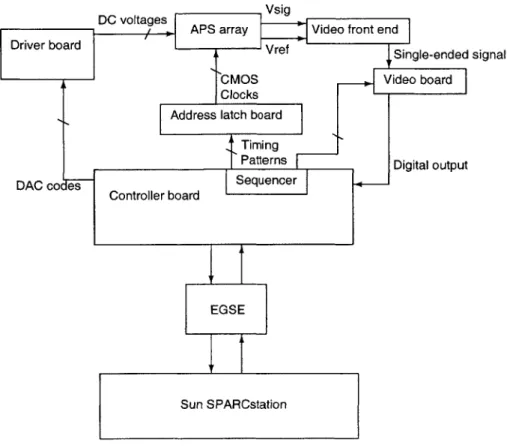
APS-1 and XIS Electronics
The reader should refer to Figure 2-3 for a schematic of APS-1.
3.2.1
APS-1 Requirements
Many CMOS-level clocks are needed for APS-1. Specifically, signals SHS, SHR, and CB, as well as COL and ROW are ordinary digital signals. Since APS-1 is a 256x256 pixel array, COL and ROW are actually internally generated, decoded versions of 8-bit column and row address signals. With some care RSTG and PG can be considered ordinary digital signals too. Counting all of these signals brings the total number of
CMOS clocks up to 21.
Not shown in Figure 2-3 is the full number of DC voltages needed. Besides VDD and
VRST, three other power supplies, VDDD, VDDMAXA, and VDDPG are needed. Internal
logic is powered by VDDD; protection diodes and some photogate circuitry are powered
by VDDPG; the output transistors (shown in Figure 2-3 with drains connected to VDD)
are actually connected to VDDMAXA. A DC bias is needed for the transfer gate TX.
To ensure optimal performance from the photogate pixels, it is possible to change the voltage that appears on the photogate when PG is high by setting the proper bias voltage on the PGBIAS line. A voltage SCP is also needed to bias the scupper, a special diode that collects excess electrons from leakage currents, especially around the edge of the device.
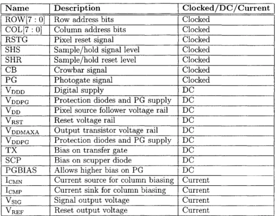
Name Description Clocked/DC/Current
ROW[7: 0] Row address bits Clocked
COL[7 : 0] Column address bits Clocked
RSTG Pixel reset signal Clocked
SHS Sample/hold signal level Clocked
SHR Sample/hold reset level Clocked
CB Crowbar signal Clocked
PG Photogate signal Clocked
VDDD Digital supply DC
VDDPG Protection diodes and PG supply DC
VDD Pixel source follower voltage rail DC
VRST Reset voltage rail DC VDDMAXA Output transistor voltage rail DC
VDDPG Protection diodes and PG supply DC
TX Bias on transfer gate DC
SCP Bias on scupper diode DC
PGBIAS Allows higher bias on PG DC
ICMN Current source for column biasing Current
ICMP Current sink for column biasing Current
VSIG Signal output voltage Current VREF Reset output voltage Current
Table 3.1: Required signals for APS-1 operation. The device requires 21 clocked
CMOS level waveforms, 9 DC biases, and 4 current sources.
Besides the CMOS clocks and DC voltages, four current sources are needed. The current load on the first source follower stage is set by 'CMN, while the load for the
second stage is set by ICMP. Current loads are required at the outputs VSIG and
VREF-A summary of required signals in shown in Table 3.1.
3.2.2
XIS Modifications
The XIS electronics have been modified so that the regulated DAC outputs from the driver board are available on the device as DC voltages. The sequencer is used to control the digital lines. The front-end of the video board has been changed to provide current source biasing for the output transistors. XIS project engineer Dick Elder assisted in the analog design work.
Vsig
DC voltages, APS array
Video front n
Driver board VSingle-ended
signal
CMOs Videbar
Clocks Address latch board
Timing
Patterns Digital output DAC co es- Sequencer
Controller board
EGSE
Sun SPARCstation
Figure 3-4: Block diagram.
Driver Board
The necessary DC voltage sources were provided by simply mapping several of the
DAC channels on the driver board to the appropriate APS-1 lines. The gain applied
to the raw DAC outputs was changed in order to provide an output range of 0 to 4 V for most signals.
Current source biasing for ICMN and 'CMP was created simply using a voltage source in series with a resistor. By making the voltage on the order of 10 V and adding a resistor on the order of 500 kQ in series, current sources in the range of 20 pA are realized. The double-cascode structure of the current mirrors means that the resistance looking into the mirror from the current source is negligible. The current can be fine-tuned by changing the applied voltage.
Some effort was required to modify current-limiting circuitry. Many of the original
addressed by changing the allowable current drive of the regulated voltages.
Sequencer Adaptation
The sequencer contains 16 programmable digital control lines, four of which are re-served for controlling the video board, leaving 12 digital signals to control the 21 required by APS-1. In order to map 12 signals onto 21, a small add-on board, the address-latch board, was designed. The address-latch board uses a 3.3V Xilinx CPLD to create the necessary outputs. One sequencer bit, B [0], was designated as the Mode bit. The value of this bit determines the functionality of the others. Given that readouts are usually sequential, the row and column addresses are rarely set to a new value, other than being incremented or decremented. This trend suggested an obvious division between the two modes.
In mode 0, five of the sequencer lines are used to directly control the more-freely varying clock signals SHS, SHR, CB, PG, and RSTG. The remaining six S-lines are used to initiate frequent row and column operations. For example, it is possible to increment the row address by setting the three bits designated for row operations to 101.b Opcodes exist for decrementing, setting to OxOG, setting to OxFF, and using a quick-load feature. Quick-load allows the user to save a desired address and then recall it later instantly. This feature may be used, for example, to store the initial column in a subarray readout. The column address is incremented as the row is read out, but at the end of the row the original column address may be restored via the quick-load feature to begin reading the next row.
In mode 1, eight of the remaining sequencer lines are mapped directly to ADD [7:0], with the value of another bit determining whether ADD maps to COL or ROW. One of the remaining two bits is used as a load signal, telling the CPLD to latch the new value into its row or column address outputs. In mode 1 the other CMOS clocks (SHS, SHR, CB, PG, and RSTG) are all forced into the unasserted state (high for PG, low for the others).
Appendix C contains a complete reference for the new board. Table C. I shows the sequencer bit reassignments more clearly. Table C.2 shows the possible operations
CB Pot. voltage 16-bit digital bias
A/D + Bit Truncation To Controller
Input amp Current switch Integrator Gain and offset Digital manipulation
Figure 3-5: Block diagram of modified video chain. The input differential amplifier subtracts Vref from Vig. The difference is integrated onto the capacitor. The crowbar is asserted, and the new values of Vret and Vig are subtracted and then integrated with the opposite polarity because of the current switch. The resulting signal is added to an adjustable offset and sent through a final gain stage to set the overall response near 1 ADU/e-. After A/D conversion a programmable bias may be subtracted. Finally, four of the 16-bits are removed and the result is sent to the controller board and eventually the EGSE and the SPARCstation.
performed on addresses while in mode 0.
Video Board
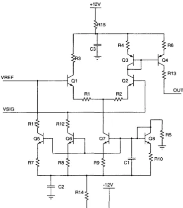
A block diagram illustrating the operation of the video board is shown in Figure 3-5. In order to accommodate the two differential outputs from APS-1, and provide
current source biasing for both, a new front end was added to the video chain. The new front end is shown in Figure 3-6. The current sources needed at the output transistors of APS-1 are provided in the form of
Q5
and Q6, nominally 5 mA each.Qi
and Q2 are a differential pair, subtracting Vrej from Vsig.Q7
andQ8
are involved in biasing, andQ3
and Q4 simply act as a mirror, flipping the direction of the output current. The gain is set such that for a typical integration time, the video board will produce a response of 1 ADU/e-.Since the video board has dual-slope integration capabilities, it may seem unnec-essary to perform a subtraction at the front end. However, when operating APS-1 in crowbar mode, there is a second signal to subtract, that of the crowbarred difference. Full operation of the video board involves integrating up the dual-slope integrator while reading the true outputs, then pulsing the crowbar and integrating down.
The video board is capable of subtracting a digital offset from the data after the
A/D conversion, but this subtraction does not help if the signal to be sampled is
+12V 15 C3 R4 R6 3 -- Q3 04R13 VREF 01 Q2 R1 R2 U VSIG R1 R12 05 06 Q7 08 R7 R8 R9 C- R10 C2 R4 -12V
Figure 3-6: New front end for video board. Q, and Q2 are a differential pair which
subtract Vrej from Vsig.
Q5
and Q6 provide the 5 mA current sources required on theoutput transistors of APS-1. The collector of
Q4
connects to the rest of the videoboard, leading into the dual-slope integrator.
approximately 82 mV, a potentiometer was added to provide an adjustable analog
offset to the signal before A/D conversion. The pot allows introduction of 2 V of
offset before the A/D converter.
The operation of the video board was verified using a dummy load consisting of 9.6 Q resistors from Vig and Vrey to ground. The voltage across these resistors provided an easy way to measure the current being drawn by Q5 and Q6. In order to simulate a signal, a 4.3 kQ resistor was connected between the CB signal from the address-latch board and Vsig.
When CB is pulsed high, the voltage at Vig increased by 7.36 mV. Assuming a responsivity of 5 pV/et, this signal represents 1473 electrons. Running the video tThis number was an initial estimate for the responsivity of APS-1. Testing has confirmed that responsivities are on the order of 5 pV/e- (see Chapter 4)..