HAL Id: tel-00520605
https://tel.archives-ouvertes.fr/tel-00520605
Submitted on 23 Sep 2010
HAL is a multi-disciplinary open access
archive for the deposit and dissemination of sci-entific research documents, whether they are pub-lished or not. The documents may come from
L’archive ouverte pluridisciplinaire HAL, est destinée au dépôt et à la diffusion de documents scientifiques de niveau recherche, publiés ou non, émanant des établissements d’enseignement et de
To cite this version:
Maxim Korytov. Quantitative Transmission Electron Microscopy Study of III-Nitrides Semiconductors Nanostructures. Condensed Matter [cond-mat]. Université Nice Sophia Antipolis, 2010. English. �tel-00520605�
UNIVERSITE DE NICE-SOPHIA ANTIPOLIS - UFR Sciences
Ecole Doctorale de Sciences Fondamentales et Appliquées
T H E S E
pour obtenir le titre de
Docteur en Sciences
de l'UNIVERSITE de Nice-Sophia Antipolis
Discipline : Physique présentée et soutenue par
Maxim KORYTOV
Quantitative Transmission Electron Microscopy Study of
III-Nitride Semiconductor Nanostructures
Thèse dirigée par Philippe VENNÉGUÈS
soutenue le 26.04.2010
Jury :
M. Martin ALBRECHT Chercheur/docteur, IKZ, Berlin Examinateur M. Michel GENDRY Directeur de Recherche, CNRS, Lyon Rapporteur M. Colin HUMPHREYS Professeur, University of Cambridge Examinateur M. Thomas NEISIUS Ingénieur/docteur, CNRS, Marseille Examinateur M. Jean-Luc ROUVIÈRE Ingénieur/docteur, CEA, Grenoble Rapporteur
M. Philippe VENNÉGUÈS Ingénieur/docteur, CNRS, Valbonne Directeur de Thèse M. Borge VINTER Professeur, University of Nice Président
ACKNOWLEDGEMENTS
The present thesis has been carried out in the Center de Recheche sur
l'Hétéro-Epitaxie et ses Applications (CRHEA) of the Centre National de la Recherche Scientifique
(CNRS). I would like to thank all people from the CRHEA laboratory for their support and concern.
I thank Michel Gendry and Jean-Luc Rouvière for accepting to be a member of the jury and reporting this work. My acknowledge also to Martin Albrecht, Colin Humphreys,
Thomas Neisius and Borge Vinter for their participation in my jury.
I feel sincere gratitude to Philippe Vennéguès, who familiarized me with various techniques of transmission electron microscopy and successfully supervised my work during these three years. Due to him I have mastered a complicated, but an exciting profession of researcher.
Julien Brault and Thomas Huault I want to thank you for growing the top-quality
samples and for being open for discussions on any epitaxy-related topics. Special appreciations to Julien for providing me essential papers on the nitride semiconductor growth. I also thank a lot Benjamin Damilano for always giving competent answers to my diverse questions. I want to express my gratitude to Mathieu Leroux, for explaining me the finest nuances of photoluminescence, as well as for critical corrections of this manuscript and for his remarks to my thesis presentation.
I would like to thank people with whom I have pleasure to work side by side on the transmission microscope of our laboratory: Olivier Tottereau for introducing me into TEM samples preparation and providing a comprehensive support for any event of live and
Jean-Michel Chauveau for fruitful discussions on the physical background of transmission
electron microscopy and numerous aspects of reliable high-resolution imaging.
I thank Luan Nguyen and Stéphane Vézian for complementary characterisation of the studied samples. Thanks to them and other people (Christian Morhain, Jesús
Zúñiga-Pérez, Denis Lefebvre, Sylvain Sergent, Aimeric Courville, Martin Jouk ...) for keeping
me an superb company during my stay in Valbonne. Special thanks to Boris Poulet for his incredible efforts in teaching me French.
I am also thankful to Isabelle Cerutti, Michèle Pefferkorn and Anne-Marie
Galliana for their administrative support and for easy solving of everyday problems. I
acknowledge Jean-Yves Duboz for competent direction of the CRHEA laboratory and for giving me an excellent opportunity to work in it.
This thesis gave rise to collaboration with other laboratories. Many thanks to Jorge
Budagosky from University of Valencia for his extensive strain computations. I also express
my gratitude for Vincenzo Grillo from National Research Centre for doing quantitative analysis of HAADF images. And I thank Mohammed Benaissa from Centre National pour la Recherche Scientifique et Technique in Rabat for EELS analysis, which is shown in this work.
Last but not least, I thank French national project METSA for providing me a unique possibility to work on the microscope facilities of CEA-Grenoble and CP2M centre in Marseille. The experimental results obtained in this thesis were considerably enriched due to the employment of these state-of-art microscopes.
RÉSUMÉ
Cette thèse est dédiée à l’étude et à la caractérisation de boîtes quantiques (BQs) GaN réalisées sur une couche épaisse d’Al0.5Ga0.5N. Une BQ se comporte comme un puits de
potentiel qui confine les porteurs de charges dans les trois dimensions de l'espace. Le spectre d’énergie d’exciton localisé dans une BQ dépend fortement de sa taille, qui est de l'ordre de quelques nanomètres.
La compréhension des mécanismes de croissance et des propriétés physiques et structurelles des objets nanométriques, telles que des BQs, nécessite l’utilisation d’outils de caractérisation adaptés à leur faible taille. La microscopie électronique en transmission (MET), largement employée dans ce travail, est une des rares techniques qui permettent ce genre d’études.
Le premier chapitre est consacré à l’introduction des fondements physiques de la microscopie électronique en transmission et à ses modes de fonctionnement. La technique de microscopie électronique en transmission haute résolution (METHR) et les facteurs limitant la résolution du microscope sont discutés en détail. Ensuite, les aspects de microscopie quantitative, tels que la simulation des images METHR et les méthodes de mesure de contrainte de la maille atomique à partir d’images METHR sont présentés. Deux techniques complémentaires au METHR, notamment l’imagerie en contraste de Z en mode balayage (STEM-HAADF) et la spectroscopie des pertes d'énergie (EELS) sont introduites à la fin de ce chapitre.
Dans le deuxième chapitre les champs d'application des nitrures d’éléments-III et certains problèmes fondamentaux liés à leur croissance épitaxiale sont discutés. Après cela, deux techniques de la croissance de ce type d’hétérostructures - l’épitaxie par jets moléculaires (EJM) et l’épitaxie en phase vapeur d’organo-métalliques (EPVOM) - sont
présentées. Ce chapitre se termine par la description des propriétés structurales des matériaux nitrures, y compris leur structure cristalline et les propriétés élastiques.
Dans le troisième chapitre, l'adaptation de l'imagerie METHR pour l'étude des matériaux à base de GaN est présentée. Tout d’abord, le moyen d'évaluation de la composition chimique dans une hétérostructure par la mesure des contraintes de la maille atomique à partir d’images METHR est décrit. L'effet de la distorsion de la maille atomique d’une couche mince due au désaccord paramétrique est pris en compte de manière analytique. Un rapport numérique entre le paramètre de réseau local et la composition des alliages InxGa 1-xN/GaN et AlxGa1-xN/Al0.5Ga0.5N est déterminé. L'influence des incertitudes des constantes
élastiques ainsi que l'effet de la relaxation de surface sur la précision de la détermination de la composition sont discutés.
Ensuite, une comparaison de deux techniques de mesure de contrainte, l'analyse des phases géométriques (GPA) et la méthode de projection, est présentée. Pour réaliser le traitement des images HRTEM dans l'espace réel (méthode de projection) un script dédié a été développé. Les deux méthodes ont été appliquées à des images modèles afin d'évaluer leurs performances pour la mesure des variations rapides de contrainte et pour le traitement des images bruitées. Il a été montré que la méthode GPA peut créer des fluctuations artificielles là où la contrainte varie rapidement. La méthode de projection est capable de mesurer les variations rapides de contrainte à l'échelle atomique, mais sa précision diminue considérablement pour les images bruitées.
Les effets des conditions d'imagerie sur les mesures de contrainte ont été mis en évidence dans la dernière partie de ce chapitre. Les images METHR en axe de zone et hors axe de zone ont été simulées par le logiciel Electron Microscopy Software (EMS) en utilisant les paramètres d'imagerie typique pour un microscope JEOL 2010F et un microscope Cs-corrigé Titan 80-300. Le rôle critique de l'épaisseur de l'échantillon pour l’imagerie quantitative METHR en axe de zone a été montré. Les gammes de défocalisation appropriées pour une détermination fiable des déplacements atomiques pour certaines épaisseurs d’échantillon ont été déterminées. La même étude a été faite pour des images METHR acquises hors axe de zone. Les conditions d'acquisition METHR adaptées aux mesures de contrainte ont été appliquées pour l'étude des BQs GaN/AlGaN.
Cette étude, présentée dans le quatrième chapitre, a révélé plusieurs phénomènes originaux pour les nitrures d’éléments III. Un changement de forme des BQs de surface de pyramides parfaites à pyramides tronquées avec l'augmentation de l'épaisseur nominale de GaN déposé a été observé. Le recouvrement des BQs par une couche d’AlGaN mène à une modification de leur forme de pyramide parfaite à pyramide tronquée. Dans le même temps, le volume moyen des BQs augmente. Un comportement similaire a été révélé pour des BQs GaN recouvertes par de l’AlN.
Une séparation de phase a été observée dans les barrières AlGaN recouvrant les BQs avec formation de zones riches en Al au-dessus des BQs et de régions riches en Ga placées autour des zones riches en Al. La concentration en Al dans les zones riches en Al est d'environ 70% et elle diminue avec la distance à la BQ; la concentration en Ga varie de 55% à 65%. Les facettes latérales des zones riches en Al sont bien définies, leur forme et leur taille sont similaires à celles des BQs au-dessus desquelles elles sont placées. Une séparation de phase a également été observée dans les échantillons avec des boîtes quantiques anisotropes (quantum dashes).
Les observations en microscopie électronique en transmission à balayage en mode Z-contraste (STEM-HAADF) ont fourni une preuve indépendante du phénomène de séparation de phases dans les barrières AlGaN. De plus, l'intensité des images HAADF a été convertie en compositions locales en gallium, à l’aide de simulations du signal HAADF. La concentration moyenne en Al de 70% dans les zones riches en Al obtenue par l'analyse HAADF a été confirmée par spectroscopie de pertes d’énergie électronique. En outre, l'analyse précise du changement de l'énergie de plasmon a révélé une diminution progressive de la composition en Al avec l’augmentation de la distance à la BQ.
Pour expliquer les phénomènes observés, différents modèles basés sur les données expérimentales ont été élaborés. Nos explications sont fondées sur le principe de minimisation de l'énergie totale des BQs. La variété des formes des BQs de surface est expliquée par la compétition entre l'énergie de surface et l'énergie élastique accumulée dans les BQs. L'augmentation du volume des BQ pendant leur recouvrement est expliqué par le transport de GaN de la couche de mouillage vers la BQ, qui peut aussi être relié à une baisse de l'énergie
élastique. Une séparation de phase dans les barrières AlGaN est aussi expliquée par la relaxation de la contrainte introduite par la présence des BQs.
Plusieurs voies, basées sur les résultats de cette étude et en vue de l’amélioration des propriétés des dispositifs optoélectroniques sont proposées. Par exemple, la fabrication de BQs sans couche de mouillage est une approche perspective pour augmenter l’efficacité de photoluminescence.
Contents
ACKNOWLEDGEMENTS... III
RÉSUMÉ... V
INTRODUCTION ... 1
Chapter I TRANSMISSION ELECTRON MICROSCOPY ... 5
1.1. High-Resolution Transmission Electron Microscopy ... 5
1.1.1. Evolution of Microscopy: from photons to electrons... 5
1.1.2. Electron transmission through the matter: scattering and diffraction ... 7
1.1.3. Principles of transmission electron microscopy; types of TEM contrast ... 10
1.1.4. Optical aberrations and practical resolution ... 14
1.1.5. Transfer function and information limit ... 16
1.1.6. Methods for spatial resolution improvement ... 21
1.2. Quantitative High-Resolution Transmission Electron Microscopy... 25
1.2.1. TEM contrast simulation ... 25
1.2.2. Heterostructure composition evaluation by high-resolution imaging ... 30
1.2.3. Methods of strain measurement ... 31
1.3. Complementary techniques... 36
1.3.1. High-angle annular dark-field imaging ... 36
1.3.2. Electron energy loss spectroscopy ... 38
Bibliography... 42
Chapter II NITRIDE SEMICONDUCTORS ... 45
2.1. Gallium nitride specificities and domains of applications ... 45
2.2. Growth of III-nitrides ... 47
2.2.1. Molecular beam epitaxy ... 47
2.2.2. Metalorganic vapour phase epitaxy... 48
2.3. Structural properties of III-nitride materials ... 49
2.3.1. Crystal structure ... 49
2.3.2. Elastic properties ... 52
Chapter III ADAPTATION OF HIGH-RESOLUTION TRANSMISSION ELECTRON
MICROSCOPY FOR THE STUDY OF III-NITRIDE HETEROSTRUCTURES... 57
3.1. Relation between III-nitride alloy composition and its local lattice parameter... 57
3.2. Evaluation of the strain measurement techniques ... 61
3.2.1. Strain distribution at the interfaces... 63
3.2.2. Noisy images treatment ... 69
3.2.3. Conclusion ... 76
3.3. Acquisition conditions for reliable high-resolution imaging... 78
Bibliography... 92
Chapter IV STUDY OF GaN/AlXGa1-XN QUANTUM DOTS MICROSTRUCTURE .. 95
4.1. Introduction... 95
4.2. General sample characterization ... 98
4.3. Morphology of GaN QDs ... 105
4.4. Study of the AlGaN barrier microstructure by HRTEM ... 111
4.5. AlGaN barrier composition evaluations by STEM-HAADF and EELS ... 124
4.6. Study of the QD capping ... 130
4.7. Study of the QDash morphology... 140
4.8. Discussion ... 144
Bibliography... 160
GENERAL CONCLUSION AND OUTLOOK ... 163
5.1. General conclusion ... 163
5.2. Perspectives ... 166
Bibliography... 169
APPENDICES... 171
APPENDIX A The relationship between three- and four-index notations ... 171
APPENDIX B Projection of interatomic distances along different zone axis ... 173
INTRODUCTION
This thesis is dedicated to the study of GaN quantum dots (QD) grown on AlGaN templates, which are promising for the development of high-efficient electro-optical applications. The optical properties of QD- based devices are governed by the QD morphology since the energy spectrum of localized exciton strongly depends on the QD size. The study of objects as small as QDs (their typical height is between 3 and 5 nm) requires the employment of a method, which combines atomic-scale resolution with capacities of quantitative analysis. High-resolution transmission electron microscopy (HRTEM) is the tool-of-choice for so challenging objectives.
HRTEM imaging has a wide range of applications; besides GaN, it can be employed for studying the different semiconductor systems. That is why the First Chapter is dedicated to a detailed introduction of this method. First, the background of the electron interaction with matter is given. Then, the different types of electron contrast, including high-resolution contrast, are explained. The main limitations of high-resolution microscopy and the ways of spatial resolution improvement are also described. In the same Chapter, the fundamentals for the local composition determination by means of relative atomic displacement measurement are given. A brief description of two analytical TEM techniques, which were used in this thesis, is presented at the end.
The Second Chapter is consecrated to the introduction of gallium nitride. We present the actual fields of application of this semiconductor, and some fundamental problems related with its epitaxial growth. After that, Molecular Beam Epitaxy and MetalOrganic Vapour Phase Epitaxy, the two epitaxial techniques commonly used for the GaN growth, are described. This Chapter is finished by the characterization of the structural properties of nitride materials, including their crystal structure and elastic properties.
In the Third Chapter, the adaptation of the HRTEM imaging for the study of GaN-based materials is presented. First, the principle of heterostructure composition evaluation by
means of the local lattice parameter measurement is stated. The impact of epilayer lattice distortion along the growth direction is taken into account analytically. A numerical relation between the local lattice parameter and the concentration x of InxGa1-xN/GaN and AlxGa 1-xN/Al0.5Ga0.5N alloy is finally determined.
The comparison of two strain measurement techniques, geometric phase analysis (GPA) and projection method, is then presented. Both methods are applied to a set of artificially created images in order to evaluate their performance in strain measurements at sharp interfaces and in treatment of noisy images.
The last part of the Chapter contains a validation of HRTEM acquisition conditions. On-axis and off-axis HRTEM images are simulated by Electron Microscopy Software with imaging parameters typical for a JEOL 2010F and a Cs-corrected Titan 80-300 microscopes, which were further used for experimental study. Strain maps calculated by geometric phase analysis from HRTEM images are analysed in order to determine the optimum image condition for strain measurements.
The study of GaN/AlGaN QD structures is presented in the Fourth Chapter. The Chapter is separated into several parts according to the investigation logic. The examination starts by the study of QD morphology change due to the QD burying by AlGaN and AlN layers. The AlGaN barriers microstructure is examined first by HRTEM and then by scanning transmission electron microscopy in high-angle annular dark-field (STEM-HAADF) mode. Then, the determination of the AlGaN barriers composition variations by various methods, including electron energy loss spectroscopy (EELS), is presented.
The study is continued by the investigations of the initial stages of the QD capping with an AlGaN layer. Cs-corrected HRTEM and probe-corrected high-resolution scanning TEM were employed for this aim. The examination of GaN/AlGaN QDs was completed by the study of anisotropic GaN islands.
Finally, the main results of the quantitative TEM study of GaN nanostructures are discussed and possible mechanisms of observed phenomena are proposed. Our explanations are based on the principle of total energy minimization and they can be used as a start point for more serious elaborations of the presented hypothesis.
Different people contributed to this study. The QD and QDash sample growth and primary characterisation were done in CRHEA laboratory by J. Brault and T. Huault. The computations of the strain tensor components for surface and buried QDs were performed by J. A. Budagosky (University of Valencia, Spain). The EELS experiments were carried out by M. Benaissa in the Max Planck Institute for Metals Research (Stuttgart, Germany). The quantitative analysis of HAADF images was done V. Grillo (National Research Centre S3, Modena, Italy). TEM study was done by the author together with P. Vennéguès using microscope facilities of CP2M-Marseille and CEA-Grenoble, which were available in the framework of METSA-project [http://www.metsa.cnrs.fr/].
Chapter I TRANSMISSION ELECTRON
MICROSCOPY
The first Chapter is dedicated to the introduction of transmission electron microscopy (TEM) which is the main technique employed in this thesis. In doing that, we will focus on the high-resolution mode, a technique that makes possible the visualization of the atomic structure of the studied matter. The factors determining the resolving power of the TEM will be discussed as well.
The second Section addresses the extraction of quantitative data from High-Resolution TEM (HRTEM) images. We will start by introducing the methods of TEM contrast simulation, which is indispensable for a correct interpretation of HRTEM images. Then, two methods of strain analysis will be presented.
At the end, we will describe two analytical techniques, which were used to verify and complete the results obtained by the HRTEM method: high angular annular dark-field (HAADF) and electron energy loss spectroscopy (EELS).
1.1. High-Resolution Transmission Electron Microscopy
1.1.1. Evolution of Microscopy: from photons to electrons
The human eye can only distinguish adjacent structural details if they are more than 0.08 mm apart; thus we cannot see objects thinner than a hair. A microscope (from the Greek: μικρός, mikrós i.e. "small" and σκοπεῖν, skopeîn i.e. "to see") is an instrument for viewing objects that are too small to be seen by the unaided eye.
The evolution of microscopy is many centuries old. The earliest evidence of "a magnifying device, a convex lens forming a magnified image," dates back to the “Book of Optics” published in 1021. The first multilens microscopes where developed in Holland around 1590. Fast improvement and expansion of microscopes began after Galilei invented a
device with variable distances between the object-glass and eye-glass. He also made a short-focus lens that allowed scope miniaturization.
In the twentieth century, optical microscopes reached their utmost resolution. The fact is that a light ray’s diffraction on the objective lens results in the image blurring. Rayleigh criterion yields a minimum spatial resolution Δl, i.e. the size of the smallest object that the lens can resolve:
∆l = 0.6 λ/β (eq. I-1)
where λ is the wavelength of light, and β is the collection semiangle of the magnifying lens. The Δl value is around 0.2 μm for microscopes operating in the visible spectrum. This means that ordinary optical microscopes are not suitable for investigation of nanostructured materials.1
The wavelength of X-rays varies from 0,005 to 10 nm allowing very attractive spatial resolution. Nevertheless, the quality of X-ray focusing systems limits the application of this method.
In 1924 Louis de Broglie formulated the hypothesis of wave-particle duality [1], which was confirmed experimentally three years later [2]. This inspired scientists to employ electrons as microscopic probe by using magnetic or electrostatic fields as lenses. The ultimate advantage is that the wavelength of an electron with a kinetic energy of 1keV is as small as 0.038 nm and it decreases as energy increases.
When the team of Max Knoll and Ernst Ruska, initially involved in developing a cathode ray oscilloscope [3], realized this fact, they aimed at the construction of a new electron device for the direct imaging of condensed matter. The first prototype of an electron microscope had quite a low magnification; the real TEM, with a resolving power greater than that of light was already built in 1933. Five years later a resolution of 10 nm was obtained with the first practical electron microscope built by Siemens.
From that time on, the interest in electron microscopy had increased and the method developed rapidly. At present day, the atomic structure of the majority of materials can distinctly be visualized with a spatial resolution better than 0.1 nm.
1.1.2. Electron transmission through the matter: scattering and diffraction
The electron has to be described quantum mechanically by a wave function which is a solution of the Schrödinger equation or Dirac equation. Under the typical illumination conditions of an electron microscope the incoming electron can be treated as a plane wave
Ψ = A0 exp [2πi(k0·r + φ0)] (eq. I-2)
where A0 is the amplitude, k0 is the wave vector and φ0 is the phase of the wave. The
wave function of the electron propagating through the sample has to take into account the interaction with the matter.
The ability of atoms to scatter electrons was experimentally discovered by Thomson at the beginning of the twentieth century [2]. If the re-radiated electron has the same magnitude of the wave vector (i.e. the same energy) as the incident one, then the interaction is called elastic; all other cases are called inelastic. The probability that an electron will be elastically scattered by an isolated atom is given by the scattering cross section:
2 = θ π σ V Ze (eq. I-3)
where Z is the atomic number, e is the elementary charge, V is the potential of the incoming electron and θ is the angle of scattering. As a result of the scattering, the intensity of the transmitted beam decreases, but new waves propagating in different directions arise.
In order to describe the elastic scattering of an electron in condensed matter the different scattering events have to be summed up coherently in crystals or non coherently in amorphous materials. However, an exact analytical description of the elastic scattering cross section is not available, since the interaction potential has to take into account as well the nucleus of the target atom as well as its electrons with very complex screening effects.
1
However some specialized techniques such as Near Field Scanning Optical Microscopy or Stimulated Emission Depletion Microscopy are capable to overcome the resolution limit imposed by diffraction.
Generally one can say that the cross section depends on the atomic number Z of the target atom, i.e. the heavier the atom the more probable is a scattering event. In condensed matter, the overall probability that an electron will be deflected from its initial direction is proportional to the length of his path into the substance. Thus, the thicker areas of the specimen scatter more electrons than the thinner ones.
The angular distribution of scattering events is highly inhomogeneous due to the matter periodicity, an effect which is called diffraction. The periodic spatial arrangement of atoms dictates that the outgoing waves leave the crystals only in certain directions. The fact is that the waves elastically diffracted by a set of parallel planes interfere with each other (Figure I-1). And constructive interference occurs only if the phase shift is a multiple of 2π. The diffraction angles θ which are satisfying this criterion of constructive interference are determined by the Bragg's law:
2d sinθ = n·λ (eq. I-4)
where θ is the angle between the wave vector of incident rays and the scattering planes, d is the spacing between those planes, λ is the wavelength of electrons, and n is an integer.
Figure I-1: Illustration of constructive (a) and destructive (b) interference: two incident waves with wave-length λ are diffracted at an angle 2θ. The red and green parts of the second wave show the path-wave-length difference.
(b) (a)
The same condition can be stated in terms of the wave and reciprocal lattice vectors (Laue equation):
k0 – kD = g (eq. I-5)
where g is a reciprocal lattice vector and k0 and kD are the wave vectors of the incident
and diffracted beams. Those vectors have the same modulus equal to 2π/λ, which is more than hundred times greater than the modulus of any primitive vector of the reciprocal lattice, typically few nm-1 long. It signifies that for an arbitrary orientation of k0 relative to the crystal
lattice, several diffracted beam vectors kD satisfying Laue equation can be chosen. Hereby the
incident wave always produces a set of diffracted beams.
At last, when an electron passes through the matter its phase is shifted in proportion to the specimen’s thickness and the inner potential relative to the phase of the electron passed through the vacuum (Figure I-2). Thereby the interaction of electrons with crystal is quite productive. Now let us see how the electron microscope reveals the structural information.
Figure I-2: The dotted line symbolizes electron propagation in vacuum. The solid line is the same for an electron travelling in the specimen. The effect of the wavelength decrease is exaggerated for better visualization. phase shift wavelength of free electron electron wavelength in specimen
1.1.3. Principles of transmission electron microscopy; types of TEM contrast
The incident electron wave should be highly coherent, so that the variations induced by the sample can be detected. Two fundamentally different types of electron sources are used in transmission microscopes. Thermionic emission, i.e. the electrons ejection over the potential barrier (called “work function”) is possible by heating the metals to high temperatures and application of a positive voltage. An alternative method of electron generation is field emission, the process whereby electrons are withdrawn from a sharp tip using a high electric field. In the latter case the electron beam has a higher spatial coherency and a shorter energy spread (0.3 eV as compared to 1.5 eV in the case of thermionic emission), which makes field emission guns (FEG) more favourable for high-resolution imaging, as we will see afterwards.
Then extracted electrons are accelerated to relativistic velocities by a voltage of several hundred kV applied to the anode (Figure I-3). The magnetic coils of the illuminating system perform shift, tilt and convergence of the electron beam. The specimen itself may be manipulated in three directions and tilted around two orthogonal axes.
Figure I-3: Image formation in TEM, at a first approximation, is quite similar to slide projection [4]. Both procedures require a source producing photons/electrons. The condenser lens creates parallel illumination
The objective lens focuses all beams diffracted by the sample, thus forming a diffraction pattern in the back focal plane. An objective aperture selects the beams which will contribute to the TEM image formation. Magnetic lenses of the projector system just magnify the final image, which is then viewed on a fluorescent screen or a CCD camera. The final image intensity is proportional to the square of the electron wave amplitude; whereas the wave phase is lost during the acquisition. So, what is the origin of the contrast that we see on the TEM screen?
A monocrystalline sample, aligned along one of the low index zone axis produces a diffraction pattern with a great number of reflections. Let us begin with the simplest case, considering that the objective aperture cuts off all diffracted beams.
The variations in thickness or composition along the field of view will change the transmitted beam intensity: since a thicker or heavier specimen area diffracts more electrons from their initial trajectory, the beam transmitted through such areas is less intense (Figure I-4). Due to this, the final TEM image represents the composition variations superposed on the contrast caused by the sample thickness fluctuations.
Figure I-4: The mass-thickness contrast formation: lighter or thinner zone of a monocrystalline specimen diffract less electrons than thicker or heavier one. Objective lens focuses all divergent waves, but only transmitted beam pass through the objected aperture. In the image plane, it forms an intensity profile representing mass and thickness variation in the field of view.
If the crystallographic orientation of the specimen varies, like in polycrystalline samples, zones satisfying to the Bragg's condition will diffract more electrons than others. This will change the intensity of the transmitted beam, revealing thereby the formation of diffraction contrast. Particularly, the observation of dislocations in bulk material is due to this mechanism.
Let us now assume that one diffracted beam passes through the objective aperture in addition to the transmitted beam (Figure I-5). The transmitted beam kT has the same wave
vector as the incident one k0.
ΨT = AT exp [2πi(k0·r + φT)] (eq. I-6)
The diffracted wave ΨD is described similarly, but the wave vector kD is related to k0
by equation I-5. The wave vectors of both beams have the same magnitude (i.e. the wavelength) but different directions. Thus, when converged by the objective lens, those waves will interfere. The interference image intensity equals
I = Ψ∑·Ψ∑*, Ψ∑ = ΨT + ΨD (eq. I-7)
back focal plane objective aperture
k0 kD specimen incident beam image plane k0 objective lens
The final image intensity I contains item ΨT*·ΨD + ΨT·ΨD*, which is proportional to
exp [2πi((k0-kD)·r + φT–φD)] + exp [-2πi((k0-kD)·r + φT–φD)] =
2cos (2π (g·r + φT–φD)) (eq. I-8)
The item ΨT*·ΨD + ΨT·ΨD* is responsible for the appearance of a sinusoidal
oscillation in the interference image. The fringe periodicity equals 1/g, i.e. it represents the spacing between the planes, which diffracted the beam kD. Therefore interplanar distances in
the studied material can be visualised by means of the high-resolution contrast.
When a few (or all) diffracted beams interfere in the image plane, they reveal the periodicity of planes that reflected these beams. However, the overall image intensity is more complicated than just the superposition of fringes formed by each diffracted beam. The problem is that the objective lens itself affects the amplitudes and phase of the diffracted waves; and this effect strongly varies with microscope defocus. Besides, the final image is also modulated by composition variations and thickness fluctuations, if they are present in the field of view.
Therefore, no matter how fine the high-resolution image looks, one should beware of direct interpretations. Only knowledge of exact microscope settings and simulation of HRTEM images may eliminate this uncertainty. We will return to this question when we will talk about the adaptation of HRTEM for studying GaN-based heterostructures (Section 3.3). Now let us consider the TEM resolution power and discuss its main limiting factors.
1.1.4. Optical aberrations and practical resolution
Indeed, since the relativistic wavelength of the electron accelerated by 200kV potential is as small as 2.5 pm, one can expect that the electron microscope will have a spatial resolution of the same order of magnitude. In practice, until recently, TEMs’ resolution was saturated around 200 pm.
The reason is, as we mentioned above, that the diffracted electron waves, which carry the structural information, are noticeably modified by the microscope itself. Magnetic lenses distort electron beams in the same way as common magnifying glasses deform the ray of light. The non-uniformities of the magnetic field inside the lens are described by aberration coefficients, similarly to light optics.
The imperfections of the objective lens have the most important impact on the spatial resolution, since that lens focuses diffracted beams and forms the primary image. Here we will briefly review the main aberrations that are of importance for HRTEM imaging.
• Azimuth nonuniformity of the magnetic field inside the objective lens causes astigmatism effect. The rays, propagating in non-parallel planes, will have foci at different points (Figure I-6). This effect introduces distortion of amount β∆f, where β is collection semiangle and ∆f is maximum difference in defocus induced by the astigmatism. Real lenses are described by different orders of astigmatism, accordingly to the symmetry of the distortion. Fortunately, the first order astigmatism can be properly balanced by tuning the compensating field inside the stigmator.
Figure I-6: Astigmatism effect: rays leaving the object B in the horizontal plane (red lines) are focused far from the rays lying in the vertical plane (blue lines) because of astigmatism. Dot-and-dash show optical axis of the lens.
• Radial nonuniformity of the objective lens field produces spherical aberration: parallel beams, which pass at different distances from the optic axis, fail to converge to the same focus (Figure I-7 (a)). Different orders of spherical aberration are also defined, but generally microscope performance is governed by the third-order aberration. As a result, a point source is imaged as a disk of minimum radius rS = C3β3, where C3 is the
third-order spherical aberration coefficient. Consequently, all nonperiodic details of the object are smoothed at the same amount; thereby the microscope practical resolution decreases.
• At last, the electrons with various wavelengths are deflected by magnetic lenses at different angles (see Figure I-7 (b)). The effect, called chromatic aberration, is always present since high-tension supplies have an intrinsic energy spread. The variation of the electrons’ wavelength blurs the image by an amount rC = CCβ∆E/E0, where ∆E – is the
energy spread of electrons, E0 – the initial beam energy, and Cc is the chromatic
aberration coefficient.
In this way, the objective lens magnifies the image, but confuses the finest details at the same time. This problem was formulated in Scherzer theorem saying that, neither chromatic, nor spherical aberration could be corrected by the rotationally symmetric elements [5]. As a result, the resolution of conventional electron microscopes is limited to about 100 times the wavelength of the electron.
Figure I-7: Due to the spherical aberration (a) initially collimated rays are not brought to a single focus, but have different focal distances. Chromatic aberration effect (b): electrons with smaller energy (blue line) has shorter focal length, than the higher energy ones (red line)
(b) (a)
0 10 20 30 40 50 0.0 0.1 0.2 0.3 0.4 0.5 c o n fu si o n d is c r a d iu s (n m )
collection semiangle β (mrad) diffraction limit chromatic aberration spherical aberration overall confusion
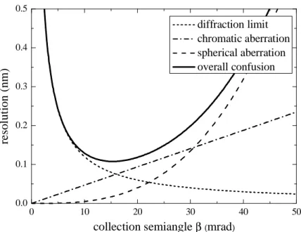
Figure I-8: Confusion disc radius as a function of the collection semiangle. The impacts of diffraction limit, spherical and chromatic aberration were plotted for JEOL 2010F with E = 200kV, energy spread = 0.8 eV, Cs = 0.5 mm, Cc = 1.1 mm.
This effect is illustrated on the example of the JEOL 2010F microscope. The diffraction limit, due to the Rayleigh criterion (eq. 1.1) equals rD = 0.6λ/β. The total radius of
the confusion disk R = (rS2 + rC2 + rD2)½ is entirely governed by the spherical aberration
(Figure I-8). And the practical resolution of the microscope is equal to the minimal radius of confusion disc Rmin ≈ 0.9 (Csλ3)¼, achieved at βopt ≈ 0.8 Cs-¼λ¼.
However, sometimes images of the crystal lattice contain some periodical features separated from one another by distances smaller than Rmin. Are such small details
distinguishable in HRTEM image still reliable?
1.1.5. Transfer function and information limit
We know that a periodic atomic lattice gives rise to strong diffraction. The diffracted beams propagate through the objective lens on slightly different paths than the transmitted one. So, once again, the role of spherical aberration is of great importance, since the electrons scattered
distance from the optical axis) transmit the smallest periodicity in the object, which defines the microscope resolution. But the outermost beams are deflected more strongly than the ones close to the optical axis, which indicates that these beams are not properly focused in the image plane. Thereby transmission of highest spatial frequencies is hindered by the objective lens aberrations.
The transfer function formalism is introduced to describe the influence of the microscope optics on the the electron wave exiting from the sample? To describe how the specimen modifies the incident uniform electron wave we should make certain simplifications. First, we presume that diffracted beam intensities are much smaller than the direct one. Thus, we focus only on the phase changes during the wave transmission through the sample; moreover we assume that those phase changes are small. This approach is known as a weak phase-object approximation (WPOA) and it only holds true for thin specimens [6]. Using WPOA the specimen function can be expressed as
f(x,y) = 1- iσVt(x,y), with σ = π /λE (eq. I-9)
where σ is the scattering constant, Vt(x,y) is the projected potential of crystal, E and λ
are the wavelength and energy of the electron wave. The image wave is given by the convolution of f(x,y) with the inverse Fourier transform of the microscope transfer function. In the WPOA only the imaginary part of the transfer function T(q) contributes to the image intensity and it can be written as:
T(q) = A(q) E(q) sinχ(q) (eq. I-10)
where q is a spatial frequency, A(q) is the aperture function, E(q) is an envelope function and χ(q) is the phase-distortion function. The aperture function shows that the objective aperture cuts off all rays diffracted above a certain angle, thus directly confining the maximum spatial frequency transmitted to the image. The phase-distortion function represents the phase difference introduced by the optical aberrations; whereas the envelope function describes their damping effect.
Let us first discuss the phase-distortion function. Every geometrical aberration contributes to the χ (q) [7], but we will consider only the main impacts:
χ(q) = πC1λq2 + ½πC3λ3q4 (eq. I-11)
where C1 is the defocus value of the objective lens, and C3 is the third-order spherical
aberration coefficient.
The behaviour of the phase-distortion for the JEOL 2010F is shown on Figure I-9 (a) (the envelope functions we will discuss bit later). The transfer function T(q) oscillates within the envelope function it reverses its sign every time when χ(q) reaches a value divisible by π. Besides, certain spatial frequencies q0, which correspond to the zeros of T(q) are not
transmitted to the image.
Moreover, the transfer function shape changes with the defocus value (compare Figure I-9 (a) and (b)). Fortunately, the operating band of T(q) can be maximized by setting the appropriate defocus value. The defocus C1Sch = -(4/3Csλ)½ proposed by Scherzer, creates the
widest band for low spatial frequencies transmission [8]. The idea is that a negative value of defocus compensates, for a certain range of q, the phase distortion due to the spherical aberration (eq. I-11).
Figure I-9 : Imaginary part of the transfer function for JEOL 2010F for 2 values of defocus. Phase-distortion function causes oscillation, whereas the envelope functions (shown by colour lines) have a
Indeed, by setting the Scherzer defocus, the first zero of T(q) is pushed towards the maximum value of q0 = 1.5 Cs-¼λ-¾ (Figure I-10). The point-to-point resolution for every
microscope is always given at Scherzer defocus.
The phase-distortion function χ(q) complicates the image contrast, whereas the envelope function E(q) limits the transfer of high spatial frequencies to the image. E(q) can be represented as a product of single envelopes:
E(q) = Es(q) Ec(q) Ed(q) Ev(q) ED(q) (eq. I-12)
where Es(q)is the spatial envelope, describing the spatial coherency of the beam, Ec(q)
is the temporal envelope describing the temporal beam coherency, Ed(q)is the specimen drift,
Ev(q)is the specimen vibration and ED(q) describes the detector performance. Specimen drift
and vibration can be minimized by maintaining a stability of the working environment. The detector envelope function is due to the delocalisation of fast electrons on the CCD camera scintillator and to the limited size of CCD pixels (Nyquist criterion). The modulation transfer function can be calibrated for a given CCD camera and taken into account for the fine analysis of HRTEM images.
Figure I-10 : Imaginary part of the transfer function for a JEOL 2010F as a function of the spatial frequency at Scherzer defocus. The point-to-point resolution corresponds to the first zero of the transfer function. The information limit (see paragraphs below) is determined by the damping effect of the envelope function.
Spatial coherency of the beam is mainly due to the angular spread of the electron source. If we consider that the electron probe has a Gaussian distribution of intensity, the spatial envelope will be
Es(q) = exp [-(πα/λ)2 (∂χ(q)/∂q)2] (eq. I-13)
where α is the semiangle describing the Gaussian distribution of electron intensity. The information throughput of a microscope can be maximized by setting it at Lichte defocus ΔfLichte = -0.75Cs(umaxλ)2, where umax is the maximum transmitted spatial frequency
[9]. At Lichte defocus the derivative of χ(u) is minimized, which decrease the damping effect of the spatial envelope. On the other hand, the use of high-coherence FEG extends the Es(q)
envelope, thus making transmission of high spatial frequencies possible at various defocuses.
The temporal envelope also damps high spatial frequency due to chromatic aberration: Ec(q) = exp [-½ (πλδ)2 q4] (eq. I-14)
where δ is the defocus spread, which is given by the equation
(eq. I-15)
here Cc is the chromatic aberration coefficient, ∆I/I is the instability of the objective
lens current, ∆E/E is accelerating tension fluctuation, and ∆U/U is the natural energy spread of the high-voltage supply. Modern transmission electron microscopes equipped with FEG have a defocus spread in the order of a few nanometres.
The spatial and temporal envelopes are shown on Figure I-11 as well as on Figures I-9 and I-10. The chromatic aberration envelope Ec(q) has, de facto, the same influence than the
aperture function A(q), since it imposes a maximum to the transmitted spatial frequency. This maximum determines the highest resolution attainable with a microscope and is called the information limit. If we neglected any other contributions to the envelope function, than the information limit due to the chromatic aberration is
Figure I-11: Imaginary part of the transfer function for JEOL 2010F at Scherzer defocus.
This equation has a fundamental value, determining the highest possible resolution achievable on a given machine (see Figure I-10). Anyhow, the extraction and correct interpretation of information lying beyond the point resolution requires serious efforts. We will return to this subject at the beginning of the next Section, when we will talk about the simulation of high-resolution images.
1.1.6. Methods for spatial resolution improvement
We finish the introduction to the HRTEM by discussing how to improve the resolution of an electron microscope. We already saw that the spherical aberration has the most important impact on the resolving power. The minimization of spherical aberration was of great interest since the TEM development. By improving the design of the objective lenses the value of the spherical aberration coefficient could be decreased down to one half of a millimetre. But as shown by Scherzer the decrease of the magnetic field in the centre of rotationally symmetric electron lenses will always produce certain spherical aberration.
Furthermore, two fundamental approaches exist to overcome the aberration limit. The pioneering idea was to increase the accelerating voltage of the electron gun up to a few MeV, decreasing thereby the wavelength of electrons below 1pm. In that way the confusion disc radius, the phase-distortion function, the point-to-point resolution and the information limit are considerably reduced. The problem was that the optical aberration increases with the accelerating voltage, diminishing thereby the positive effect of electron wavelength reduction. However, an electron beam with an energy of 1 MeV considerably damages the specimen. Nevertheless high tension TEMs are more efficient than common microscopes; and quite a number of such machines were built. But an enormous fabrication cost makes this approach economically unattractive; only few MeV-voltage TEMs are operating nowadays [10].
The alternative way consists in the correction of optical aberrations. In light optics the spherical aberration can be minimized using combination of convex and concave lenses, having opposite values of Cs. Unfortunately all magnetic lenses are convex, thus the spherical aberration coefficient is always positive. Scherzer theorem claims that the correction of Cs is possible only by the introduction of a special correcting element.
Various prototypes were suggested, but only the concept proposed by Rose [11] turned to be realizable. The principle is to introduce multi-pole elements into the microscope column. Properly tuned internal magnetic field of the multi-pole elements will strongly deflect electron beam that passes at higher distance from the optic axis. Additional electron lenses are introduced to compensate the low-order aberrations produced by multi-poles elements.
Finally overall microscope spherical aberration (objective lens + corrector) can be tuned to zero or even to a negative value with an accuracy of a few µm. In fact, all optical aberrations up to third-order can be balanced with a high accuracy.
The realization of a Cs-corrector in 1995 broke fresh ground in the field of electron microscopy. If we look again to the problem of image blurring due to the optical aberrations described in Section 1.1.5, then we will see that now the practical resolution is twice improved (Figure I-12). The minimum confusion disc radius is governed only by the chromatic aberration Rmin ≈ 1.1(λCC∆E/E0)½, where ∆E is the natural energy spread of
electron source and E0 is the beam energy. The range of optimum β is larger than in the case
0 10 20 30 40 50 0.0 0.1 0.2 0.3 0.4 0.5 re so lu ti o n ( n m )
collection semiangle β (mrad) diffraction limit chromatic aberration spherical aberration overall confusion
Figure I-12: Confusion disc radius as a function of collection semiangle for a Cs-corrected microscope. The impacts of diffraction limit, spherical and chromatic aberration were plotted for a Titan 80-300 with E = 300kV, energy spread = 0.7 eV, C3 = -0.005 mm, C5 = 4 mm, Cc = 2.0 mm. Note the difference
comparing to Figure I-8.
The transfer function of the Cs-corrected microscope is smooth and simple (Figure I-13). The spatial envelope stretches over the high-frequency part due to the phase-distortion function correction. The information limit is also significantly improved, since now it is governed only by the chromatic aberration. The foremost advantage is that the point resolution approaches the information limit. In fact, “resolution” term is no more in use, since now the microscope performance is entirely determined by the information limit which mainly due to on the electron gun energy spread, chromatic aberration coefficient and microscope stability. Modern Cs-corrected microscopes, equipped with a FEG, have information limit around 0.08 nm2.
The further improvement of microscope performance might be achieved by the compensation of the chromatic aberration. The Cs- and Cc-correctors have the a similar principle, however in the second case the electron trajectory rectification is obtained by tuneable electric fields.
2
For the time being, the ultimate information limit, as small as 50 pm, belongs to the TEAM 0.5. This 300kV microscope houses high-brightness gun with low energy spread and improved Cs corrector able to compensate fifth-order of spherical aberration. Superior machine with spherical and chromatic aberration corrector will be elaborated soon within the framework of this research project.
Figure I-13: Imaginary part of the transfer function for the Cs-corrected Titan 80-300 as a function of the spatial frequency. The C3 coefficient is -4 µm, Cc is 2 mm and the energy spread 0.7 eV. Comparing to the
JEOL 2010F (Figure I-9) the microscope passband is extended towards spatial frequencies allowing 80 pm resolution; note that the abscissa scale is twice greater to display high-frequency part of T(q).
An alternative approach is to use a monochromator, which decreases the energy spread of the outgoing electron beam. Its mode of functioning is rather simple: transiting electrons are deflected by a magnetic field and only those having required energy pass through the exit slit. The outgoing beam is less intense, but its’ energy spread is considerably reduced.
Nevertheless, machines with large spatial and temporal envelopes (considering equation I-12), are extremely sensitive to any extrinsic instabilities. Whatever the case, microscope environment should be as stable as possible. However, to achieve sub-angstrom resolution it is essential to entirely isolate sample stage from acoustic noises, ground vibrations and temperature changes. Otherwise specimen drift and vibrations will make atomic resolution unachievable. Besides, electrical supplies should provide constant voltages to electron gun and objective lens, in order to minimize the defocus spread, reducing thereby the information limit.
So, transmission electron microscopy progressed a lot since its invention in 1933. Anyhow the method is still far from being perfect and it will be certainly improved in the future. But even at the present, a non-ideal state TEM is an exclusive research tool for the characterization of materials crystal structure and obtaining unique information on the sample microstructure. In the following Section we will discuss the essential aspects of the
1.2. Quantitative High-Resolution Transmission Electron Microscopy
In the first part of this Chapter we discussed the factors governing the resolving power of TEM. Here we will talk about imaging of the specimen structure, image treatment and quantitative data extraction. Though the resolution of modern microscopes (0.08 – 0.1 nm) is few times lower than the interatomic distances of most solids (0.2 – 0.5 nm), the HRTEM images do not always represent the exact atomic structure. The factors limiting the utilization of HR microscopy and the need of image simulation are discussed first. Then we will talk about heterostructure composition determination by means of local lattice parameter. After that the techniques used for the displacement measurement from the HRTEM images will be discussed.
1.2.1. TEM contrast simulation
The ultimate aim of HRTEM imaging is the local atomic structure determination. However, the wave exiting from the sample is strongly distorted by the optical aberrations. The HRTEM image thereby depends on the shape of the transfer function, which noticeably varies with the defocus (Figure I-9).
But even the wave exiting from the object does not correspond exactly to the projected potential of the studied structure. The point is that the electron wave may diffract several times even in a thin crystal. Indeed, a diffracted beam in perfect Bragg orientation is to be diffracted again by the same set of planes (Figure I-1). Consequently the exit wave function greatly depends on the crystal thickness.
As a result, finding the true atomic positions from a HRTEM image is a very intricate objective. However, it is much easier to solve an inverse problem: to calculate a HRTEM image by the convolution of the microscope transfer function with the exit wave from an assumed atomic structure. The image simulation is realized in the following way:
• At first the assumed atomic structure is modelled.
• Next the interaction of the electron wave with the inner potential of the crystal is calculated.
• Then the exit wave is distorted during the propagation towards the image plane.
• Finally the image wave interferes following the Abbe’s theory and forms thereby the HRTEM image.
If the simulated HRTEM image differs noticeably from the experimental one, then, either the assumed atomic structure or the microscope characteristics should be modified. If satisfactory resemblance is achieved, than one may conclude that the atomic arrangement in the studied area is known. Anyhow it should be kept in mind that sometimes two different structures can produce similar images.
The effects of optical aberrations are taken into account by means of the microscope transfer function. But the exit wave can be calculated by different methods. The kinematical theory is the simplest approach to compute the amplitude of the scattering beam. It assumes that an electron beam passing through the sample will be diffracted only once and without losing energy. Thus, inelastic scattering and multiple diffraction are excluded. Such approach simplifies noticeably the calculations, but it fails completely for samples with thicknesses above 5 nm. The probability of multiple diffraction increases with the thickness, which necessitates the use of dynamical calculations.
The full description of any physical system evolution is given by the time dependent Schrödinger equation. The Bloch’s theorem proves that the wavefunction of a particle placed into a periodic potential can be described as the product of a plane wave eik·r and of a periodic function unk(r) = unk(r+R), where vector R is the period of the potential:
(eq. I-17)
By the substitution of this definition into the Schrödinger equation, the latter is reformulated into the nonlinear matrix problem of finding the electron wave vectors and the Bloch wave coefficients [12].
The total calculation time of the Bloch wave method is proportional to the cube of the number of used Bloch waves. The calculation might be notably simplified, by applying the
weak diffracted beams as small perturbations to the strong ones. A simple test allows checking if enough reflections have been introduced into the calculation: one has to repeat the routine with an additional reflection and to check that the change induced in the largest eigenvalue is smaller than a given maximum [13].
The Bloch wave method is very efficient for unit cells containing a small number of atoms. The key point is that only a small number of waves are required to fully reproduce the electron state in such structures. When the lattice parameters of unit cell increases, further reflections are required to describe it; thus the calculation time increases considerably.
The multislice technique [14,15] is better adapted to calculate the contrast created by a large set of atoms. The atomic lattice is sectioned in many slices, normal to the incident beam. The incident beam interacts with the projected potential of the first slice, thereby giving rise to a number of diffracted waves. Then all these beams propagate towards the second slice potential and scatter once again. Renewed sets of waves iterate the same sequence of propagation and interaction till it leaves the specimen.
The slice thickness is a free parameter and can be diminished, improving thereby computation accuracy. The optimal way of atomic lattice cutting is when every slice is thin enough to satisfy the weak phase approximation. This criterion is fulfilled if the product of the maximum value of the projected potential on the scattering constant σ, defined by equation I-9, is smaller than 1. The scattering constant σ is inversely proportional to the electron wavelength. For microscope operating at 200 keV, σ is close to 6.26·10-3 and for 300 keV microscope, σ equals to 5.32·10-3.
The multislice method can only be applied to orthogonal atomic lattices. The majority of structures can be reformed to orthogonal ones by addition of further atoms; but often this procedure results in noticeable enlargement of atomic cells, which increases the calculation time.
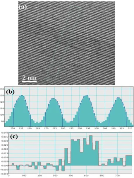
Both techniques are illustrated by the calculation of a HRTEM image from a Si crystal using the JEOL 2010F microscope configuration. The simulation was carried on the Java version of Electron Microscopy Software (JEMS) [16]. Bloch wave algorithm uses Bethe's approach with 25 strong reflections. No sub-slicing is introduced for the multislice calculations.
Figure I-14: A series of high-resolution TEM images of a Si crystal along the [1,1,0] zone axis simulated by Blochwave (a), (c), (e) and Multislice techniques (b), (d), (f). The sample is 10 nm thick and the microscope parameters are those of the JEOL 2010F: E=200kV, energy spread = 0.8 eV, Cs = 0.5 mm and objective aperture = 30 nm-1. (a) and (b) images are taken at Scherzer defocus (-43.4 nm), (c) and (d) at zero defocus, and (e) and (f) at a defocus of -29 nm. The exact positions of atoms are indicated by the colour spots.
The projections of the distances between two neighbouring Si atoms along the [1,1,0] zone axis is as small as 0.136 nm. A JEOL 2010F microscope having a point-to-point resolution of 0.194 nm is not able to resolve this distance. Thus, two atomic columns are represented by a single white spot (Figure I-14).
Both Bloch wave and multislice techniques produce rather similar images, while image contrast varies noticeably with changes of defocus. In the images acquired at Scherzer defocus (figures I-14 (a) and (b)) intensity maxima are between the atomic columns. Whereas pictures calculated at zero defocus (figures c and d) exhibit an opposite contrast. The defocus value of -29 nm (figures e and f) produces images with a double number of intensity maxima.
Only the combination of electron micrograph with image simulation techniques can provide reliable structural information. The best precision is obtained when a series of images with different defoci is matched with simulated data.
HRTEM images simulated using parameters of Cs-corrected machines are shown on Figure I-15. The point-to-point resolution of the Titan 80-300 with a Cs-corrector is about 0.08 nm, thus the Si doublets are instantly resolved (Figure I-15 (a)). Improving of the beam temporal coherency pushes information limit toward higher spatial frequencies, making image sharper (figures (b) and (c)). A hypothetical, aberrations-free machine produces an ultimate image (figure d).
So, HRTEM image simulation is essential to understand or even predict the contrast of experimental images. Another approach, called exit wave reconstruction, is capable to calculate back numerically the exit wave function [17]. This procedure is based on the treatment of a large focal series of images, supposing that all acquisition parameters are precisely known. Exit wave reconstruction was not used in this work, but image simulation was largely employed.
Figure I-15: High-resolution TEM images of a Si crystal simulated by the Blochwave technique for a Titan 80-300 microscope equipped with a Cs-corrector. Image (a) is for a machine operating at 300 keV with C3
= -5 µm, C5 = 4 mm, Cc = 2 mm, and energy spread = 0.7 eV. Further image improvement can be achieved
either be correcting the chromatic aberration up to Cc = 5µm (b) or by decreasing the energy spread up to 0.3 eV (c). An ultimate image (d) was obtained on the ideal machine free of any aberrations and having an energy spread of 0.01 eV.
1.2.2. Heterostructure composition evaluation by high-resolution imaging
High-resolution transmission electron microscopy has a broad field of applications. The central objective of this thesis is an investigation of the structural properties and compositions of group-III nitride heterostructures. For doing this, we will focus on the measurement of the local lattice parameter (LLP), i. e. the distance between two adjacent atomic planes. The LLP varies with the chemical composition. The Vegard’s law, which holds true for a majority of compounds, states a linear dependence between the lattice parameter a of a ternary alloy AxB1-xC and its concentration x.
a(AxB1-xC) = a(BC) + x · [ a(AC) - a(BC) ] (eq. I-18)
Using this equation the composition variation may be determined with a spatial resolution equivalent to an interatomic distance. It has to be noted that, despite the high lateral resolution, the LLP measured by HRTEM is always averaged through the TEM sample thickness (5-50 nm).
This approach is widely used to study compound structures, where composition variations may exist. Two main aspects giving rise to a deviation from the linearity of the Vegard’s law should be considered. First, the stress field, which generally exists in heterostructures, may cause a displacement of atoms from their initial positions. However, if the atomic displacement is regular, the change of LLP can be analytically taken into account. The simplest case is the biaxial stress, which generally takes place in thin epilayers. We will produce some formulas in Section 2.3.2, when we will talk about the strain states in nitride films.
Another phenomenon that often affects the atomic arrangement is a surface relaxation effect in thin crystals. Atoms situated near free surfaces have a higher freedom to move. This results in additional atom displacements which minimizes the total stress energy. The TEM sample has to be thinned down to 5 - 50 nm, otherwise electron waves will be highly absorbed. So the number of near-surface atoms may be quite high (ratio surface/volume). The effect of atomic reorganization is non-linear and depends strongly on sample composition,

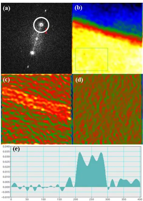
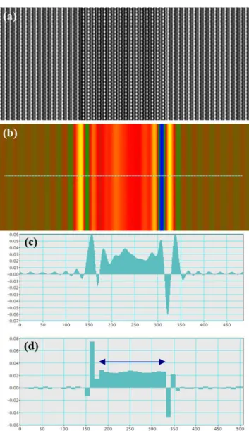
![Figure III-3: Actual HRTEM image of a GaN/AlGaN interface taken along the [1100] direction (a)](https://thumb-eu.123doks.com/thumbv2/123doknet/12991959.379387/72.892.137.796.576.1029/figure-actual-hrtem-image-algan-interface-taken-direction.webp)
![Figure III-23: Atomic structure of an AlGaN/GaN/AlGaN interface projected along the [1100] zone axis](https://thumb-eu.123doks.com/thumbv2/123doknet/12991959.379387/90.892.137.831.736.1003/figure-iii-atomic-structure-algan-algan-interface-projected.webp)