RESEARCH OUTPUTS / RÉSULTATS DE RECHERCHE
Author(s) - Auteur(s) :
Publication date - Date de publication :
Permanent link - Permalien :
Rights / License - Licence de droit d’auteur :
Bibliothèque Universitaire Moretus Plantin
Institutional Repository - Research Portal
Dépôt Institutionnel - Portail de la Recherche
researchportal.unamur.be
University of Namur
Graphene-coated holey metal films
Reckinger, Nicolas; Vlad, Alexandru; Melinte, Sorin; Colomer, Jean-François; Sarrazin,
Michaël
Published in:
Applied Physics Letters
DOI:
10.1063/1.4808095 Publication date:
2013
Document Version
Peer reviewed version
Link to publication
Citation for pulished version (HARVARD):
Reckinger, N, Vlad, A, Melinte, S, Colomer, J-F & Sarrazin, M 2013, 'Graphene-coated holey metal films: Tunable molecular sensing by surface plasmon resonance', Applied Physics Letters, vol. 102, no. 21, 211108. https://doi.org/10.1063/1.4808095
General rights
Copyright and moral rights for the publications made accessible in the public portal are retained by the authors and/or other copyright owners and it is a condition of accessing publications that users recognise and abide by the legal requirements associated with these rights. • Users may download and print one copy of any publication from the public portal for the purpose of private study or research. • You may not further distribute the material or use it for any profit-making activity or commercial gain
• You may freely distribute the URL identifying the publication in the public portal ?
Take down policy
If you believe that this document breaches copyright please contact us providing details, and we will remove access to the work immediately and investigate your claim.
arXiv:1304.3291v2 [cond-mat.mes-hall] 23 May 2013
Graphene-coated holey metal films: tunable molecular sensing
by surface plasmon resonance
Nicolas Reckinger,1,† Alexandru Vlad,2,† Sorin Melinte,2 Jean-Fran¸cois Colomer,1 Micha¨el Sarrazin1,†∗
1
Research Center in Physics of Matter and Radiation (PMR), Department of Physics, University of Namur, 61 rue de Bruxelles, B-5000 Namur, Belgium
2
Institute of Information, Communication Technologies, Electronics and Applied Mathematics, Electrical Engineering, Universite catholique de Louvain, Louvain-la-Neuve, B-1348, Belgium and
†These authors contributed equally to this work
We report on the enhancement of surface plasmon resonances in a holey bidimensional grating of subwavelength size, drilled in a gold thin film coated by a graphene sheet. The enhancement originates from the coupling between charge carriers in graphene and gold surface plasmons. The main plasmon resonance peak is located around 1.5 µm. A lower constraint on the gold-induced doping concentration of graphene is specified and the interest of this architecture for molecular sensing is also highlighted.
†These authors contributed equally to this work.
PACS numbers: 78.67.Wj, 73.20.Mf, 42.79.Dj, 07.07.Df
Plasmonic devices offer valuable platforms for a wide range of emerging molecular detection schemes. Among such applications, biosensors are very promising espe-cially from the point of view of lab-on-a-chip (LOC) technologies.1Indeed, plasmon resonances are
character-ized by both a strong electric field and a great sensi-tivity to environmental conditions. As a consequence, adsorbed species can be detected through the reso-nance wavelength shift. In addition, the strong elec-tric field enhancement allows for surface enhanced Ra-man spectroscopy, which can be used for single molecule detection.2
Surface plasmons (SPs) require specific conditions to be excited. For instance, in the Kretschmann configura-tion, a light beam is totally internally reflected in a prism on which a metallic film is deposited and triggers the gen-eration of SPs.3In a holey metal film, SPs can be excited
by a normal incidence light beam.4Light is scattered due
to the corrugations and the evanescent diffraction orders can excite SPs.5 For a metallic layer accommodating an
array of holes with subwavelength size, it is possible to probe SPs by simply measuring the intensity of the trans-mitted light. Such a simple configuration is much more practical in the LOC context and it has been widely stud-ied since the pioneering work of Ebbesen et al. in 1998.4
Recent theoretical works have shown that doping can induce SP modes in graphene.6–8 Graphene, which
ap-pears as a monoatomic layer made of sp2 carbon atoms
in a hexagonal lattice configuration, presents a plethora of amazing properties.9 In that context, SPs have been
observed for graphene doped by charge transfer from metal thin films,10–13 external atoms14 or electrostatic
gating15,16. It has been also suggested that SPs could
be excited in graphene on a periodically structured
∗e-mail: michael.sarrazin@unamur.be
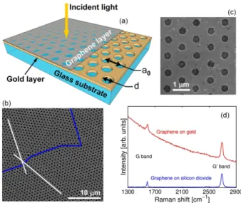
FIG. 1: (Color online). (a) Sketch of the device. A microscope glass slide with a thickness of 1 mm is coated with a 25-nm-thick gold film. The metallic film is perforated by a hexag-onal array of holes with a grating parameter a0 = 980 nm.
The hole diameter is d = 405 nm. The perforated gold film is coated by a graphene sheet. (b) Scanning electron microscopy (SEM) picture of two domains (delimited by blue lines) with different orientations (white straight lines) in the holey gold film. (c) SEM top view of the final device. (d) Raman spec-troscopy of the synthesized graphene layer, transferred on gold and on silicon dioxide.
substrate17,18 or via regular patterns in graphene.19–25
A recent experimental result showed that graphene SPs can be excited in a Kretschmann configuration using graphene deposited on a planar gold layer.10 A different
approach26 was used in which SP resonance tunability
was achieved by electromagnetic field coupling between a graphene sheet and SPs excited in gold nanoparticles.
opti-2
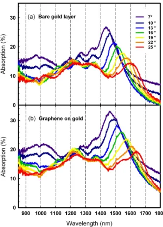
FIG. 2: (Color online). Optical characteristics of the device. Absorption spectra of the uncoated holey gold film (a) and of the graphene-coated device (b) for various incidence angles.
cal device constituted by a planar hexagonal array of subwavelength-sized holes in a gold thin film functional-ized with a graphene layer. The entire device is built on a glass substrate. Resonances of the device are measured for various incidence angles. It is shown that graphene enhances the plasmon resonances and induces a redshift of the resonance wavelength. This plasmonic device used as a molecular sensor displays a wavelength shift which is highly sensitive to environmental conditions.
Figure 1(a) gives a conceptual illustration of the nanos-tructured plasmonic platform. It was fabricated by us-ing colloidal nanosphere lithography. Briefly, polystyrene spheres (980 nm in diameter, Microparticles GmbH) were deposited on soda-lime glass plates via an interfacial self-assembly protocol.27,28 Reactive ion etching using O
2
chemistry (Oxford Plasmalab, 100 W RF power, 100 sccm O2, 25 mTorr, 12 min) was used to reduce the
size of the colloids to half the nominal diameter. Sub-sequently, 2 nm of Ti followed by 25 nm of Au were deposited using physical vapor deposition. The liftoff was performed using adhesive tape and ultrasonication in dichloromethane. Figure 1(b) shows a Scanning Elec-tron Microscopy (SEM) top view of the array made of large periodic crystal-like domains.
Graphene was synthesized by atmospheric pressure chemical vapor deposition at 1000◦C on copper foils with
methane as carbon source.29–31 The copper foil was
in-serted into a quartz reactor inside a hot-wall furnace. After annealing at 1000◦C for 30 min under argon (500
ml/min) and hydrogen (100 ml/min), methane was ad-mitted (0.5 ml/min) for 15 min to grow graphene. It was next cooled down rapidly under argon and hydrogen. After spin-coating a polymethyl methacrylate (PMMA) film over graphene,32the copper foil was etched in
aque-ous ammonium persulfate. Next, the PMMA/graphene stack was rinsed in distilled water and transferred onto the holey gold/glass substrate. The PMMA film was then removed by soaking into acetone and finally blown dry with nitrogen. Figure 1(c) shows a SEM top view of the resulting device. In addition, a reference sample with graphene over planar gold was fabricated. Graphene was also transferred on silicon dioxide (300-nm-thick) for Raman inspection. The detection of G (∼1590 cm−1)
and G′ (∼2690 cm−1) bands testifies of the presence
of graphene (see the Raman spectra in Fig. 1(d), for graphene over planar gold and silicon dioxide). No disorder-related D band (∼1350 cm−1) is observed,
sug-gestive of virtually defect-free graphene.
Optical characterization was carried out at various incidence angles by using an integrating sphere setup mounted on a Perkin-Elmer Lambda 750S UV/Vis/NIR spectrophotometer. The sample was positioned such that the light source faces the graphene surface at normal inci-dence. Figure 2(a) shows the absorption (AB) of the bare
holey gold film (i.e. without graphene). The extinction of the graphene-coated holey gold film is shown in Fig. 2(b) (AG). The typical absorption peaks denote surface
plasmon polaritons.5 As it can be observed, graphene
induces a redshift of the plasmon resonance peaks and dramatically enhances the absorption of the device up to 40% (see also Fig. 3(a)). It is noteworthy that the main plasmon resonance peak is located around 1.5 µm, close to the wavelength range of interest to optoelectronic applications.
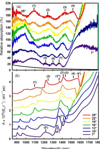
The relative absorption R, calculated as R = (AG −
AB)/AB, is shown in Fig. 3(a). The role of SPs is
an-ticipated from the relative shift of the peaks in Fig. 3(a) for the considered incidence angles. In addition, the rel-ative absorption of a graphene layer deposited on un-structured gold (black curve in Fig. 3(a)) shows a weak enhancement by contrast with the corrugated gold film. Since corrugated metallic films allow for SP modes, it is a strong argument for the coupling between SPs on gold and graphene. To further support this, we have run numerical simulations based on a homemade code which rests on a rigorous coupled wave analysis (RCWA) method.5 By considering the frequency − and position
− dependence of the electric field E(ω, r) inside a given material, the absorbed power is given by:33
Pabs= − ε0ω 2 Z V ε′′(ω, r) |E(ω, r)|2d3r (1) where ε0 is the vacuum permittivity, ε′′ is the imaginary
FIG. 3: (Color online). (a) Relative absorption of the graphene-coated versus uncoated gold for various incidence angles. The black curve represents the relative absorption for a non structured metal film. For the sake of clarity, each curve is shifted vertically by 25 units with respect to the pre-vious one. (b) Numerical simulation of the absorption of the graphene-coated device for various angles of incidence. For the sake of clarity, each curve is shifted vertically by 0.5 units with respect to the previous one.
part of the relative permittivity of the medium (here the graphene layer), and V its volume. This formula can be expressed according to the real part of the medium conductivity, i.e. γ′= ε
0ωε′′. For a two-dimensional-like
medium, such as graphene, we get Pabs= − 1 2 Z S γ′(ω, ρ) |E(ω, ρ)|2 d2ρ (2)
with S the surface, ρ the position vector along the graphene layer, and where γ′ is the real part of the
graphene conductivity.34,35 γ′ can be restricted to the
intraband term:7,35,36 γ′= e 2E F π~2 τ−1 (ω2+ τ−2) (3)
with ~ the reduced Planck constant, e the electron charge, EF the Fermi level, and τ the relaxation time.
FIG. 4: (Color online). Zeroth order transmission through graphene-coated gold (red curves) and bare gold (black curves) devices. A significant peak shift occurs when ethanol is deposited on the devices (dashed curves) by contrast with cases without ethanol (solid curves). Compared to the bare gold device, for the device coated with graphene, the wavelength-shift is enhanced by 33%. Peaks retrieve their initial positions after few minutes when ethanol is fully evap-orated.
The intraband approximation is legitimate since no res-onance occurs below 900 nm, suggesting that EF ≥ 0.7
eV,19,36
corresponding to a charge density n ≥ 4×10¹³
cm−2.7 Albeit large, these values are in agreement with
those achieved in other works.11,12,14
Let us now consider E(ω, r) as the electric field of the electromagnetic wave scattered at the air/gold in-terface without graphene. We suppose that such an electromagnetic field is not significantly modified by the graphene layer as a first approximation. In addition, we suppose that the extrinsic conductivity of graphene due to the gold film can be considered as uniform, i.e. γ′
does not depend on ρ. The incident power is given by Pin= (1/2)σcε0Ein2, where c is the speed of light, σ is the
area of the unit cell of the array, and Einthe electric field
amplitude of the incident wave. Then, the absorption of graphene is defined as A = |Pabs| /Pin, and assuming that
we work at frequencies ω ≫ τ−1, we get
A = K0λ2 1 E2 in 1 σ Z S|E(λ, ρ)| 2 d2ρ (4)
where λ is the wavelength (λ = 2πc/ω) and K0 =
e2E
Fτ−1/(4π3c3ε0~2). Except for K0, which is a mere
factor of proportionality, A can be easily computed nu-merically using our homemade RCWA code, allowing to propagate the electromagnetic field on a bare perforated gold layer on glass. The permittivities of materials are taken from the literature.37 In Fig. 3(b), we display the
calculated quantity A/EFτ−1 for different incidence
an-gles. Markers (noted as numerals, from (1) to (7), from (3′) to (7′), and (3′′)) have been added in Figs. 3(a) and
4 matches very well the experimental data shown in Fig.
3(a). This supports the supposition that the enhance-ment is due to graphene conductivity coupled with sur-face modes, i.e. SPs at the gold/air intersur-face. We note a few discrepancies, for instance, the peak at wavelength (3) seems to result from two shifted resonances at wave-lengths (3′) and (3′′). Peaks at wavelengths (5) to (7)
also appear shifted to wavelengths (5′) to (7′). These
dif-ferences between experiment and numerical simulations are due to the fact that we consider a perfectly periodic hole array in our simulation while the real one is consti-tuted of a set of many crystal-like domains (see the SEM picture in Fig. 1(b)). In addition, the retroactive role of the graphene layer on the electric field E(ω, r) is not considered. The present theoretical results indicate that graphene must be doped in order to support SPs (here, the doping is extrinsic and provided by the gold layer). Indeed, if K0 = 0 (i.e. absence of doping) there is no
absorption. In addition, the intraband approximation is also supported by the fact that the interband term35,36
is unable to reproduce the experimental patterns shown in Fig. 3(a).
In the following, we show that graphene-coated holey gold films enhance the wavelength shift against the envi-ronment changes proving the versatility of this configura-tion for LOC sensing applicaconfigura-tions. We have analyzed the response of the devices in the presence of ethanol at the main plasmon resonance around 1.5 µm. Ethanol is first spread on the graphene side of the device. To avoid thin film interferences due to a thick ethanol layer, a delay of 30 seconds is set to allow ethanol to partially evaporate. This preserves an adsorbed layer with a subwavelength thickness. Transmission is then recorded. Figure 4 dis-plays the response of the devices when in presence of ethanol. The zeroth order transmissions at normal in-cidence are plotted where a typical peak is observed for wavelengths around a SP resonance.5 The transmission
peak for both types of gold samples (graphene-coated and bare) is redshifted when exposed to ethanol. However, the graphene-coated sample shows a higher wavelength-shift sensitivity − the resonance peak wavelength-shift being 33% greater than for the bare device. After complete evapo-ration of ethanol, the peaks retrieve their initial position.
Note that the wavelength shift as well as the transmission decrease (i.e. the absorption enhancement) are related. Indeed, the surface plasmon wave vector ksp must verify
ksp =
k//+ g
, where k// is the parallel component of
the wave vector of the incident light wave with respect to the interface, and g is a vector of the reciprocal lattice. For the smallest non trivial vector g and for normal inci-dence, the wavelength λspfor which a plasmon resonance
occurs can be roughly approximated by:3,33
λsp≈ a0 √ 3 2 Re s εd+ i γ′ d ωε0 (5)
where εdis the permittivity of the dielectric environment
which surrounds the metallic layer and γ′
d the
conduc-tivity of the dielectric, which depends on the graphene layer conductivity. If γ′ increases, the optical
absorp-tion increases (since γ′= ε
0ωε′′), but λsp is also shifted.
Moreover, the ethanol layer present on the device alters the combined permittivity εd and also causes shift and
intensity changes.
In summary, nanostructured hybrid graphene-gold ar-chitectures enhance the wavelength shift in plasmonic sensors. The simple graphene-coated metal grating de-vice allows for a facile optical characterization at normal incidence, without the need of a complex Kretschmann configuration, greatly improving the portability of the measurement setup. Moreover, the rich graphene sur-face chemistry offers unique functionalization protocols, enlarging further the sensor’s versatility.38
The authors acknowledge C. N. Santos and B. Hack-ens for their help with Raman measurements, as well as F. J. Garcia de Abajo and L. Henrard for useful discus-sions and comments. This work was supported by the Belgian Fund for Scientific Research (F.R.S.-FNRS) un-der the FRFC contract ”Chemographene” (convention No.2.4577.11) and via the FRFC project No.2.4510.11. A.V., S.M. and J.-F.C. acknowledge F.R.S.-FNRS for fi-nancial support. This research used resources of the In-teruniversity Scientific Computing Facility located at the University of Namur, Belgium, which is supported by the F.R.S.-FNRS under the convention No.2.4617.07.
1
H. Craighead, Nature 442, 387 (2006).
2
M. Moskovits, Rev. Mod. Phys. 57, 783 (1985).
3
H. Raether, Surface Plasmons on Smooth and Rough Sur-faces and on Gratings (Springer-Verlag, Berlin and Heidel-berg, 1988).
4
T. W. Ebbesen, H. J. Lezec, H. F. Ghaemi, T. Thio, and P. A. Wolff, Nature 391, 667 (1998).
5
M. Sarrazin, J.-P. Vigneron, and J.-M. Vigoureux, Phys. Rev. B 67, 085415 (2003).
6
S. H. Abedinpour, G. Vignale, A. Principi, M. Polini, W.-K. Tse, and A. H. MacDonald, Phys. Rev. B 84, 045429 (2011).
7
M. Jablan, H. Buljan, and M. Soljacic, Phys. Rev. B 80, 245435 (2009).
8
F. H. L. Koppens, D. E. Chang, and F. J. Garcia de Abajo, Nano Lett. 11, 3370 (2011).
9
A. K. Geim and K. S. Novoselov, Nature Mater. 6, 183 (2007).
10
O. Salihoglu, S. Balci, and C. Kocabas, Appl. Phys. Lett. 100, 213110 (2012).
11
P. A. Khomyakov, G. Giovannetti, P. C. Rusu, G. Brocks, J. van den Brink, and P. J. Kelly, Phys. Rev. B 79, 195425 (2009).
12
Karpan, J. van den Brink, and P. J. Kelly, Phys. Rev. Lett. 101, 026803 (2008).
13
Z. Fang, Y. Wang, Z. Liu, A. Schlather, P. M. Ajayan, F. H. L. Koppens, P. Nordlander, and N. J. Halas, ACS Nano 6, 10222 (2012).
14
S. Y. Shin, N. D. Kim, J. G. Kim, K. S. Kim, D. Y. Noh, Kwang S. Kim, and J. W. Chung, Appl. Phys. Lett. 99, 082110 (2011).
15
J. Chen, M. Badioli, P. Alonso-Gonzalez, S. Thongrat-tanasiri, F. Huth, J. Osmond, M. Spasenovic, A. Centeno, A. Pesquera, P. Godignon, et al., Nature 487, 77 (2012).
16
Z. Fei, A. S. Rodin, G. O. Andreev, W. Bao, A. S. McLeod, M. Wagner, L. M. Zhang, Z. Zhao, M. Thiemens, G. Dominguez, et al., Nature 487, 82 (2012).
17
X. Zhu, W. Yan, P. U. Jepsen, O. Hansen, N. A. Mortensen, and S. Xiao, Appl. Phys. Lett. 102, 131101 (2013).
18
A. Ferreira and N. M. R. Peres, Phys. Rev. B 86, 205401 (2012).
19
Yu. V. Bludov, A. Ferreira, N. M. R. Peres, and M. I. Vasilevskiy, Int. J. Mod. Phys. B 27 1341001 (2013).
20
A. Yu. Nikitin, F. Guinea, F. J. Garcia-Vidal, and L. Martin-Moreno, Phys. Rev. B 84, 161407(R) (2011).
21
A. Yu. Nikitin, F. Guinea, F. J. Garcia-Vidal, and L. Martin-Moreno, Phys. Rev. B 85, 081405(R) (2012).
22
A. Yu. Nikitin, F. Guinea, and L. Martin-Moreno, Appl. Phys. Lett. 101, 151119 (2012).
23
V. V. Popov, T. Yu. Bagaeva, T. Otsuji, and V. Ryzhii, Phys. Rev. B 81, 073404 (2010).
24
V. V. Popov, O. V. Polischuk, A. R. Davoyan, V. Ryzhii,
T. Otsuji, and M. S. Shur, Phys. Rev. B 86, 195437 (2012).
25
S. Thongrattanasiri, F. H. L. Koppens, and F. J. Garcia de Abajo, Phys. Rev. Lett. 108, 047401 (2012).
26
J. Niu, Y. J. Shin, Y. Lee, J.-H. Ahn, and H. Yang, Appl. Phys. Lett. 100, 061116 (2012).
27
A. Vlad, A. Fr¨olich, T. Zebrowski, C. A. Dut¸u, K. Busch, S. Melinte, M. Wegener, and I. Huynen, Adv. Funct. Mater. 23, 1164 (2013).
28
A. Vlad, I. Huynen, and S. Melinte, Nanotechnology 23, 285708 (2012).
29
X. Li, W. Cai, J. An, S. Kim, J. Nah, D. Yang, R. Piner, A. Velamakanni, I. Jung, E. Tutuc, et al., Science 324, 1312 (2009).
30
B. Wu, D. Geng, Y. Guo, L. Huang, Y. Xue, J. Zheng, J. Chen, G. Yu, Y. Liu, L. Jiang, and W. Hu, Adv. Mater. 23, 3522 (2011).
31
N. Reckinger, A. Felten, C. N. Santos, B. Hackens, and J.-F. Colomer, arXiv:1303.3951 [cond-mat.mtrl-sci].
32
A. Reina, X. Jia, J. Ho, D. Nezich, H. Son, V. Bulovic, M. S. Dresselhaus, and J. Kong, Nano Lett. 9, 30 (2009).
33
J. D. Jackson, Classical Electrodynamics (Wiley, 1998).
34
N. W. Ashcroft and N. D. Mermin, Solid State Physics (Saunders, Philadelphia, PA, 1976).
35
G. W. Hanson, J. Appl. Phys. 104, 084314 (2008).
36
G. W. Hanson, J. Appl. Phys. 103, 064302 (2008).
37
E. D. Palik, Handbook of Optical Constants of Solids (Aca-demic, Boston, 1985).
38
W. Gao, L. B. Alemany, L. Ci, and P. M. Ajayan, Nature Chem. 1, 403 (2009).