ALGERIAN DEMOCRATIC AND POPULAR REPUBLIC MINISTRY OF HIGH EDUCTATION AND SCIENTIFIC RESEARCH
UNIVERSITY FRERES MENTOURI CONSTANTINE 1 FACULTY OF SCIENCES EXACTES
PHYSICS DEPARTMENT
Order N°: Series:
THESIS
PRESENTED TO OBTAIN DOCTORATE OF SCIENCE DIPLOMAT SPECIALTY
ÉNERGÉTIQUE
THEME
Study of the effect of grading in composition on the performance of
thin film solar cells based on AlGaAs and CZTSSe, a numerical
simulation approach
By Nadia MESSEI Defended on: 12 / 06 / 2016
Jury committee:
President: N.ATTAF --- Prof. Univ. frère Mentouri Constantine Advisor : M.S.AIDA --- Prof. Univ. frère Mentouri Constantine Examiners: C.AZIZI --- Prof. Univ. Oum El Bouaghi
A.ATTAF --- Prof. Univ. Biskra S.RAHMANE --- Prof. Univ. Biskra
To my parents
To my twin, the source of beauty in my life,
To you khadidja & soumia
Acknowledgements
Firstly, I would like to thank professor Mohamed Saleh AIDA, the Advisor of this thesis.
I would like to thank all members of the examining committee of this thesis.
Thank you, professor Nadir ATTAF for agreeing to serve as president of the jury. Thank you, professors: Cherifa AZIZI, Abdallah ATTAF and Saad RAHMAN for
agreeing to evaluate this work.
A big thank you, to Professor M. Burgelman for allowing me to use SCAPS1D and for being always opens to discussions and confrontation on different themes of my work.
Thank you Lamine, Faiza and Sabrina for being in my side every time I needed in the preparation of the manuscript
Table of Contents
Chapter 1: Background
1.1 Overview ...1
1.2 Advantages and disadvantages of solar energy ...2
1.2.1 Advantages ...2
1.2.2 Disadvantages ...2
1.3 Energy from solar cell ...3
1.3.1 Cells, modules, panels and Systems ...3
1.4 The history of solar cells ...4
1.5 Aim of this work ...5
References of chapter1 ...8
Chapter 2: Photovoltaic cell and phenomena Overview ...9
2.1 Semiconductors ...9
2.1.1 What is a semiconductor material ...9
2.1.2 Electron and hole concentration ...10
2.2 PN junction ...13
2.3 Current in diode ...14
2.4 Types of Semiconductor Junctions ...15
2.4.1 Homojunction and Heterojunction ...15
2.4.2 Metal-semiconductor contact ...16
2.4.2.1 Ohmic contact ...17
2.4.2.2 Tunnel contact ... ...17
2.5 Solar cell efficiency ...18
2.6 Detailed Balance and Main Assumptions ...20
2.7 Light absorption ...22
2.7.1 The sun ...22
2.7.2 Optical Absorption in Semiconductor ...23
2.8 Solar cell generations ... ...24
2.9 Thin film solar cell ... ...25
2.9.2 Crystalline silicon thin film solar cells ... ...26
2.9.3 Amorphous and microcrystalline silicon thin film solar cells ... ...26
2.9.4 Cadmium telluride solar cells ...27
2.9.5 Chalcopyrite ...27
2.10 Other solar cell types……… ...28
2.10.1 Organic Photovoltaics OPV...28
2.10.2 III-V Tandem and Multijunction Cells...29
2.10.3 Dye-sensitised solar cell (DSSC)...29
2.10.4 Quantum Well Solar Cells...29
2.10.5 Concentrator photovoltaics CPV...30
References of chapter 2 ...32
Chapter 3: Graded solar cell 3.1 An alloy and a compound ...34
3.2 Uniform or graded absorber ...34
3.3. CZTSSe solar cell ...35
3.3.1 Overview ...35
3.3.2 Material properties ...36
3.3.2.1 The Crystal Structure of CZTS ...36
3.3.2.2 Band Energies ...38
3.3.2.3 Point Defects ...40
3.3.2.4 Optical properties ...41
3.3.2.5 Grain boundaries ...41
3.3.2.6 Synthesis techniques ...42
3.3.3 CZTSSe graded solar cell ...42
3.4. AlGaAs solar cell ... ...44
3.4.1 Overview ...44
3.4.2 Material parameters ...45
3.4.2.1 The Crystal Structure of AlGaAs ...45
3.4.2.2 Band Energies ...46
3.4.2.3 Point Defects ...47
3.4.2.4 Other important properties: ...48
3.4.3 Graded AlGaAs solar cell ...48
Chapter 4: Simulation process
Overview ...54
4.1 Modeling, simulation or analysis? ...54
4.2 Basic modeling techniques ...55
4.3 Commonly used simulation software ...55
4.3.1 AMPS ...55 4.3.2 wxAMPS ...56 4.3.3 PC1D ...56 4.3.4 AFORS-HET ...57 4.3.5 ASA ...57 4.3.6 SCPS 1D ...58
4.4 Simulation process of CZTS cell ...58
4.4.1 The beginning ...58
4.4.2 Solar cell definition ...59
4.4.3 Contact ...61
4.4.4 How to obtain a graded layer? ...62
4.4.4.1 The grading laws ...63
4.4.4.2 Parameter grading ...66
4.4.4.3 Band diagram of a graded layer ...67
4.4.4.4 Defects and recombination ...69
4.4.5 The IV-panel ...69
4.4.6 The QE-panel ...70
References of chapter 4 : ...71
Chapter 5: Results and discussion 5.1 CZTSSe solar cell ...73
5.1.1 Cell structure ...73
5.1.2 Uniform cell ...73
5.1.3 Cell with profile (a) ...75
5.1.4 Cell with profile (b) ...78
5.2 AlGaAs ...81
5.2.1 Cell structure ...81
5.2.1.1 Optimization of layers thickness ...81
5.2.1.2 Effect of the capping layer ...82
5.2.2.1 Front grading of p layer ...83
5.2.2.2 Back grading ...85
5.2.3 Double grading ...87
5.2.4 Fully graded cell ...88
5.3 Conclusion ...90
5.3.1 CZTSSe cell ...90
General Introduction
The huge increase of energy prices has amplified the attention for renewable energies significantly in particular solar cells. This is reflected in the important enlargement of research in this area. Thin-film solar cells technology still offers the possibility of reducing the manufacturing costs. To increases the conversion efficiency of a thin film solar cell, several optimization techniques have been proposed. One of the promising methods to enhance the performance of third generation solar cells is to use compositionally graded profils in the structure of a solar cell. The grading of the band-gap and other semiconductor properties, especially doping concentration, had been proposed a long time ago in order to improve solar cells efficiency both experimentally and via computer simulation. Direct band gap compounds are suitable to implement band-gap engineering in graded solar cells.
In this thesis we chose to test the effect of several graded schemes on the performance of AlGaAs and CZTSSe thin film solar cell using numerical simulation. A steady progress has been made in these two types of solar cells and a large number of papers were published. This dissertation is proposed to fill some of the gaps that exist between the state-of-the-art experimental graded solar cells and their device physics. The level of difficulty involved is the expensive analytical treatment and, therefore, numerical approaches are primarily employed.
The quaternary p-type semiconductors Cu2ZnSn (S1-ySey )4 (CZTSSe) with favorable
direct band-gab is derived from CuInGaSe2 (CIGS) and keep its noticeable
photovoltaic properties, but also contains earth abundant and safe elements like (Zn) and (Sn). The pre-factor of absorption coefficient for the CZTSSe alloys thin film is large enough (>104cm-1). Despite The discovery that a CZTS thin film has an optimum direct band gap of 1.45eV for solar cells was made in 1988, the efficiency of CZTSSe solar cells remains under that of devices with absorbers produced from older materials such as CIGS, CdTe and GaAs. The current highest photoelectric conversion efficiency of CZTSe and CZTS based solar cells is the range of 12.6% and 9.1% respectively. This efficiency is very low compared with its theoretical limit.
Usually, in uniform solar cell, the band-gap energy Eg of the absorber material is
optimized by the well known exchange between high current for low Eg and high
voltage for high Eg. To achieve further increase in the efficiency, grading of the band
gap Eg(x) and most other materials properties in the cell thickness direction (x) can be
involved. This can be achieved by using a compositional graded absorber. The idea is to increase the short circuit current Jsc while maintaining the open circuit voltage by
realizing a well suited band gap profile Eg(x).
AlyGa1-yAs compounds (y<0.45) are also suitable to implement band-gap
engineering in graded solar cells because they are characterized by a direct band-gap , an efficient optical absorbers as required , a tiny change in lattice constant ( 1%) and an advanced technology. The greatest obstacle which faced the success of GaAs cells was the high cost of a single crystal GaAs substrate. Researchers are exploring several approaches to reduce the cost of GaAs devices. One of those approaches is growing of GaAs cells on cheaper, removable and re-usable GaAs substrates. In this thesis we have studied the effect of fully graded scheme on AlyGa1-yAs solar cell using
numerical simulation with SCAPS1D. The gradient is simultaneously in the composition and in doping concentration
This thesis is divided into two virtual parts:
First Part embraces chapters 1 and 2. It is dedicated to the theory of Photovoltaic solar cell. Part II includes the chapters 3, 4 and 5. It refers to discuss materials, structures and simulation. Every chapter in the second part is divided in two divisions, one relating to CZTSSe and the other to AlGaAs.
Chapter 1 presents an overview on the stat-of-the-art of renewable energy especially photovoltaic solar cells and a clarification of the aim of this thesis.
Chapter 2 deals with photovoltaic process and phenomena. Where important principles and properties of semiconductors and solar cells were briefly reviewed as far as these is helpful for the understanding of this manuscript.
Chapter 3 Deals with graded thin film solar cell. This chapter starts first by describing what means a compound, an alloy, a graded material, a uniform layer and a graded layer. In addition it includes a brief description of state-of-the-art of
Cu2ZnSn(S1-ySey)4 (CZTSSe) and AlyGa1-yAs (AlGaAs) alloys and graded solar cells.
Finely, useful compositionally graded profiles were proposed.
Chapter 4, in this chapter our simulation process was discussed and a brief description of commonly used PV simulation software. Then, the simulation package SCAPS1D was largely described using the case of CZTSSe as solar cell material. The second case, AlGaAs, follows the same steps considering the existing differences between the two materials which were explained in chapter 3.
Chapter 5 summarizes all our simulation results and discussions in both cases, CZTSSe and AlGaAs graded solar cells. First, we have checked the effect of all possible and/or efficient graded profiles (back, front, double and fully) on the performance of our CZTSSe solar cell. As result we can say that an appropriate graded profile can ameliorate extremely the performance of the solar cell. Second, we have tested the effect of fully graded profile on AlGaAs cell. In order to do this step it was necessary to check at first the effect of commonly used front and back profiles. As result an appropriate fully graded strategy can leads to better solar cell performances.
All discussion, in this work, is limited to open circuit voltage Voc, short circuit
current Jsc , efficiency η and Fill Factor FF.
Table caption
Table 1.1 : Confirmed terrestrial cell and sub-module efficiencies.
Table 1.2 : Confirmed terrestrial module efficiencies.
Table 1.3 : “Notable exceptions”: “top ten” confirmed cell and module results.
Table 2.1 : The main characteristics of thin film solar cells.
Table 3.1 : Optical band gap energy of Kesterite and stannite CZTS1-ySey alloy.
Table 4.1 : Available basic grading laws in SCAPS.
Table 5.1 : Properties of kesterite and stannite uniform solar cells by SCAPS.
Figure caption
Figure 1.1: World energy consumption by source , Renewable for 19% .
Figure 1.2 : a) Simplified scheme of a solar cell , b) solar cell module.
Figure 1.3: a) Highest confirmed efficiencies for solar cells. c) concentrator cells and modules.
Figure 2.1: The range of doping levels used in c-Si.
Figure 2.2: The important points regarding p-type (n-type) semiconductors
Figure 2.3: Formation of a p-n junction in the Schottky approximation.
Figure 2.4: The three types of semiconductor heterojunction organized by band alignment
Figure 2.5: Band diagrams for straddling -gap heterojunction
Figure 2.6: Illustration of metal–semiconductor contact in thermal equilibrium
Figure 2.7: Side view schematic of a solar cell showing the various layers and the equivalent circuit of solar cell
Figure 2.8: (a) Light and dark J-V curves for an ideal solar cell
Figure 2.9: Several steps of photovoltaic conversion
Figure 2.10: Maximum theoretical efficiency (Shockley–Queisser limit) for solar cells under AM1.5 illumination without concentration
Figure 2.11: Energy losses at earth atmosphere
Figure 2.12: Direct band gap semiconductor and indirect band gap semiconductor
Figure 2.13: The three generation of solar cell
Figure 2.14: a) Cross section of typical multijunction solar cell based on a-Si:H.
Figure 3.1: Relationship between binary, ternary, and quaternary semiconductors to produce Cu2ZnSnS4 , starting from a II–VI parent compound
Figure 3.2: The crystal structure of Cu2ZnSnS4 .
Figure 3.3: The calculated band alignment between CdS, Cu2ZnSnS4 , Cu2ZnSnSe4
and CuInSe2.
Figure 3 .4: The ionization levels of intrinsic defects in the band-gap of Cu2ZnSnS4.
Figure 3.5: Absorption coefficients α as a function of photon energy ħω for CZTS and of CZTSe.
Figure 3.6: Schematic structure of CZTSSe solar cell commonly used
Figure 3.7: Schematic diagram of the band alignment in the Se-graded CZTSSe absorber layer
Figure 3.8: (A) The diamond structure. (B) The zincblende .
Figure 3.9: Lattice parameter a as a function of y for AlyGa1-yAs at 300 K.
Figure 3.10: Band structure of AlyGa1–yAs
Figure 3.11: Energies of the lowest direct EgD and indirect gaps EgID at 300 K
Figure 3.12: Uniform p-i-n AlGaAs/GaAs solar cell under equilibrium .
Figure 3.13: Characteristic graded structure profiles. a-front, b-double, c-back, d-fully graded.
Figure 4.1: Define the problem and the working point
Figure 4.2: Defining a solar cell structure
Figure 4.3: Contact properties panel
Figure 4.4 : Setting the composition grading y(x). Select a grading law for the composition
Figure 4.5 : The shallow donor (acceptor) graded density
Figure 4.6 : Setting the absorption constant from file (left) or from model (right).
Figure 4.8 : Adding, editing and removing defects.
Figure 4.9 : Visualization of the solar cell parameters
Figure 4.10 : Ordinate choices on the QE-panel
Figure 5.1:a) Schematic material structure of graded CZTSSe solar cell, b) schematic diagram of the band alignment between CdS, CZTS and CZTSe
Figure 5.2: The CB alignment at the CZTSSe/CdS interface
Figure 5.3: Effect of grading with profile (a) on the four parameters. strategy 1
Figure 5.4: Effect of grading with profile (a) on the four parameters. strategy 2
Figure 5.5: Effect of grading with profile (b) on the four parameters, strategy 1
Figure 5.6: Effect of grading with profile (b) on the four parameters, strategy 2
Figure 5.7: Quantum efficiency versus GaAs buffer thickness in μm.
Figure 5.8: Band gap diagram of p-i-n solar cell with front band gap grading.
Figure 5.9: Jsc, and efficiency in function of Wpg.
Figure 5.10: Jsc, efficiency and FF in function of ΔEc.
Figure 5.11: Jsc, efficiency and FF in function of Wng.
Figure 5 12 : Jsc and efficiency in function of ΔEv .
Figure 5.13 : Energy band diagram of the totally graded structure.
Figure 5.14 : Quantum efficiency of the fully graded device as function of wavelength.
Chapter
1
1 1.1 Overview
Humans utilize energy in several different forms in order to run machinery and accomplish different tasks. As shown in Figure 1.1[1] modern energy consumption mainly depends on fossil fuels that are limited and can cause environmental issues such as greenhouse gas emission and global warming. This coupled with high oil prices, peak oil, and increasing government support has stimulated nations to search for alternate, clean, and renewable energy sources.
Renewable energy is energy which comes from natural resources such as sunlight, wind, rain, tides, and geothermal heat, which are renewable (naturally replenished). Renewable energy sources are even larger than the traditional fossil fuels and in
2
theory can easily supply the world’s energy needs. 89 PW of solar power falls on the planet’s surface. While it is not possible to capture all, or even most, of this energy, capturing less than 0.02 per cent would be enough to meet the current energy needs [2]. Energy from the sun or solar energy, provide consistent and stable source of solar power throughout the year. Solar electricity, including solar photovoltaics, is expected to make a great contribution as a major energy source, providing a share of about 20% of global electric power in 2050 and about 70% in 2100 [3].
1.2 Advantages and disadvantages of solar energy
In spite of solar energy has many advantages but also it has some disadvantages, here some of them and not all:
1.2.1 Advantages
a. Solar energy is free although there is a cost in the building of ‘collectors’ and other equipment required to convert solar energy into electricity or hot water.
b. However, solar collectors and other associated equipment are manufactured in factories that cause some pollution. Solar energy does not cause pollution.
c. In far areas where it is too expensive to extend the electricity power grid the Solar energy can be used.
d. Many everyday items such as calculators and other low power consuming devices can be powered by solar energy effectively.
e. It is estimated that the world’s oil reserves will last for 30 to 40 years. On the other hand, solar energy is infinite.
1.2.2 Disadvantages
a. Solar energy can only be harnessed when it is sunny and daytime.
b. Solar systems are relatively expensive to manufacture although prices are falling speedily.
c. Solar power stations can be built but they do not match the power output of similar sized conventional power stations. They are also very expensive.
d. In countries such as in Europe, the unreliable climate means that solar energy is also unreliable as a source of energy. Cloudy skies reduce its effectiveness.
e. Collectors are usually arranged together, so large areas of land are required to capture the suns energy.
3
f. Solar power is used to charge batteries so that solar powered devices can be used at night. However, the batteries are large and heavy and need storage space. They also need replacing from time to time.
1.3 Energy from solar cell
Photovoltaic (PV) devices called solar cells generate electricity directly from sunlight via an electronic process that occurs naturally in certain types of material, called semiconductors. Photons hit and ionize semiconductor material on the solar panel, causing external electrons to break free of their atomic bonds. The electrons are forced in one direction creating a flow of electrical current. Electrons in these materials are freed by solar energy and can be induced to travel through an electrical circuit, powering electrical devices or distribution electricity to the grid as shown in Figure 1.2.
1.3.1 Cells, modules, panels and Systems
Various solar cells in an integrated group, all oriented in one plane, constitute a solar photovoltaic panel or solar photovoltaic module as shown in Figure 1.2.b. Photovoltaic modules often have a piece of glass on the sun-facing side, allowing
a) b)
4
light to go by while protecting the semiconductor wafers. Solar cells are generally connected in series and parallel circuits or series in modules, creating an additive voltage. Connecting cells in parallel yields a superior current; however, problems such as shadow effects can makes troubles [1].
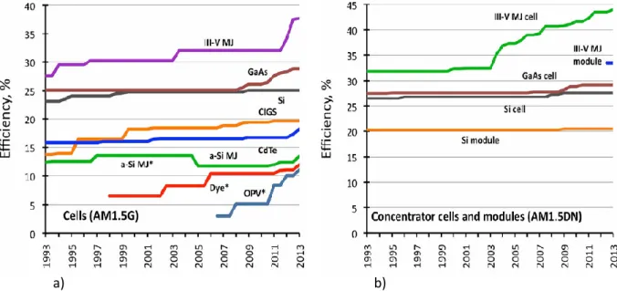
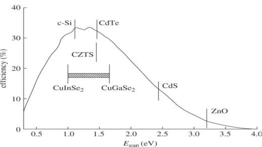
Figure 1.3 shows the full range of PV cell types with the world record efficiencies achieved by each over the past twenty years, as catalogued by Green and his colleagues. These are research cell, not production cell,
1.4 The history of the solar cells
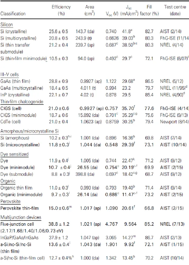
Table 1.1, 1.2 and 1.3 summarized the best solar cell and module efficiencies achieved until now, those tables was taken from according to ref [4]. But it takes a long time to attain those values. In this section we present the long history of photovoltaic cell [5-7]:
The beginning was in 1839, when A.E. Becquerel discovered the photovoltaic effect, by illuminating two electrodes with different types of light. In 1873 W. Smith discovered the photo conductivity of Selenium. But just in 1876 Selenium produces electrical current when it is exposed to sun light. In 1883 Fritts made the description of the first selenium solar cells and in 1894 he constructed the first true solar cell of 1% efficiency where he coated the selenium with a thin layer of gold. Later in 1905
Figure 1.3: a) Highest confirmed efficiencies for solar cells. c) concentrator cells and modules.
5
A. Einstein claimed that light consists of “packets” or photons what explained the absorption of the photons regarding to the frequency of the light. In 1916, R. A. Millikan provided experimental proof of the photoelectric effect. In 1918 J. Czochralski developed a way to grow single-crystal silicon. This increased the efficiency of the silicon-based cells. In 1930 W. Schottky and others developed a theory of metal-semiconductor barrier layers. In 1932 the photovoltaic effect in cadmium sulfide (CdS) was discovered. In 1950 Bell Labs produce solar cells for space activities. In1953 D. Trivich made the first theoretical calculations of the efficiencies of various materials of different band-gap widths based on the spectrum of the sun. In 1954 Bell Labs produced a handmade silicon solar cell with 4% efficiency which later increased to 11%. It was the first material to directly transfer enough sunlight into electricity. In 1954 a cadmium Sulphide PN junction was produced. In 1958 the first PV-powered satellite, Vanguard I, was launched. In 1959 Explorer-6 was launched with a PV array. In 1970 First highly effective GaAs Heterostructure solar cells are created by Z. Alferov. In 1976 D.Carlson and C. Wronski produced the first amorphous silicon cells with 1.1% efficiency. In 1980 the first (Cu2S and CdS) thin-film solar cell exceeds 10% efficiency. In 1981 P. M.Cready
builds the first powered aircraft and in 1982 H. Tholstrup drives the first solar-powered car. In 1989 Reflective solar concentrators are first used. In 1991 Efficient Photoelectrochemical cells (PEC) was developed and the Dye-sensitized solar cell (DSC), also called Grätzel cells, was invented. In 1994 the NREL develops a solar cell made from gallium indium phosphide and gallium arsenide that becomes the first one to exceed 30% conversion efficiency.
1.5 Aim of this work
The major challenge of photovoltaic is to produce more efficient solar cell with less prices. One of the promising methods to enhance the performance of third generation solar cells is to use compositionally graded layers. The aim of this work is to study the effect of grading in composition on two types of solar cells, AlGaAs and CZTSSe. The gradient is simultaneously in the composition and in doping concentration in AlGaAs solar cell and just in composition in the second cell. Our simulations were done using SCAPS 1D simulation software.
6
Table 1.1: Confirmed terrestrial cell and submodule efficiencies measured under the global
AM1.5 spectrum (1000 W/m2) at 25 °C. CIGS = CuInGaSe2; a-Si = amorphous
7
Table1.2: Confirmed terrestrial module efficiencies measured under the global AM1.5 spectrum (1000 W/m2) at a cell temperature of25 °C , a-SiGe = amorphous
silicon/germanium/hydrogen alloy; Effic. = efficiency; (t) = total area [4]
Table1.3 :“Notable exceptions”: “top ten” confirmed cell and module results, not class records measured under the global AM1.5 spectrum (1000Wm_2) at 25 °C CIGSS = CuInGaSSe; CZTSS = Cu2ZnSnS4 ySey; CZTS = Cu2ZnSnS4 [4]
8 References of chapter1
[1] https://en.wikipedia.org/wiki/Renewable-energy/ (04:2016)
[2] S. C. Bhatia , Advanced renewable energy systems, Part – I, Woodhead Publishing India Pvt. Ltd. ( 2014).
[3] M.D. Archer & M. A.Green, Clean electricity from photovoltaics, 2nd Edition, Imperial College Press (2015).
[4] M. A. Green, K. Emery, Y. Hishikawa3, W. Warta & and E. D. Dunlop. Solar cell efficiency tables (version 46), Prog. Photovolt: Res. Appl, 23:805–812 (2015).
[5] http://www.sunlightelectric.com/pvhistory.php/ (04/2016).
[6] https://en.wikipedia.org/wiki/Timeline_of_solar_cells/ (04/2016).
[7] Paul A. Lynn, Electricity from Sunlight: An Introduction to Photovoltaics, Wiley (2010).
Chapter
2
Photovoltaic cell and
phenomena
9 Chapter 2: Photovoltaic cell and phenomena Overview
In the majority of solar cells the absorption of photons, which results in the generation of the charge carriers, and the subsequent separation of the photo-generated charge carriers take place in semiconductor materials. Therefore, the semiconductor layers form the heart of the solar cell. In this chapter we will discuss the most essential semiconductor properties, the solar cells and their performances.
2.1 Semiconductors
2.1.1 What is a semiconductor material?
A number of materials such as copper pass electric currents very easily. Therefore they have very low resistivity and so are classed as conductors. Other materials such as plastics have very high resistivity so do not conduct electricity. These materials are called insulators. Materials such as Silicon and Germanium that have a resistivity mid-way between the conductors and insulators do conduct current, but very poorly at normal room temperatures, and so these are called semi-conductors.
Today, semiconductor materials are contained in approximately all electronic devices. We present here some of those devices not all:
• Photonic devices capture light (photons) and convert it into an electronic signal. They are used in camcorders, solar cells, optical fibers.
• Optoelectronic emitters convert an electronic signal into light. Examples are light-emitting diodes (LED), laser printers, and eye surgery.
• Flat-panel displays create an image by controlling light that either passes through the device or is reflected off of it.
• In field-effect devices the conductivity is modulated by applying an electric field to a gate contact on the surface of the device. As example the MOSFET (metal-oxide semiconductor field-effect transistor).
• Quantum devices are based on quantum mechanical phenomena, like tunneling of electrons through potential barriers which are impenetrable classically.
10
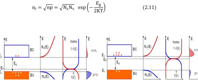
The defining property of a semiconductor material is that it can be doped with donor atoms and/or acceptor atoms that adjust its electronic properties in a controllable way. Figure 2.1 shows the range of doping that is used in case of crystalline –Si [1].
2.1.2 Electron and hole concentrations
In undoped (intrinsic) semiconductor material, if (n) is the electron concentration and (p) is the hole concentration:
If the concentration of donor atoms (ND) is greater than the concentration of acceptor
atoms (NA), then the semiconductor material is n‐type, (n) is greater than (p):
If NA > ND, then the semiconductor material is p‐type, because p > n: ƒ
To comprehend the behavior of semiconductors, we need to explore what we mean by the electron and hole densities in the conduction and valence bands, respectively. the notion of energy density of states N(E) is a parameter gives the number of states (per unit volume and per unit energy) between E and E+dE: Nc(E) (respectively, Nv(E)) physically represents the “room” available for electrons (resp. holes) in the
11
conduction band (resp. valence band)[2]. For energies that are close to the extrema of these two bands, the density of states has a quadratic dependence with E:
Where =h/2 is the normalized Planck constant and mc (resp. mv) is the average effective mass of the conduction band (resp. of the valence band). For a direct gap semiconductor, mc (resp. mv) is the effective mass of an electron me (resp. a hole mh) in the crystal. The density of states is not the only information that we need to identify the number of electrons and holes present in each band. Furthermore, we have to know the probability for an electron to occupy a level with a given energy E. This probability is given by the Fermi-Dirac distribution function [2-5]:
Where K=1,38.10-23 JK-1 is the Boltzmann constant, T the absolute temperature (K) and EF the Fermi energy. 1-f(E) gives The probability for a hole to occupy a level of energy E because a hole, in definition, is the absence of an electron. The electron
density n [cm-3] ( resp. the hole density p) in the conduction band( valance band ) is obtained by integrating, over the range of energies accessible by electrons in the band, the number of states that may be occupied by electrons of energy E, weighted by the probability to “find” an electron having this given energy :
12
In a p-type semiconductor at thermal equilibrium there are a lot of free holes in other word (p) is approximately equal to the density of doped acceptor impurities [2-5], giving rise to the p-type conductivity. The hole concentration p is given by
As the acceptor density increases, EF tends towards EV. In addition, there is a very
small amount of free electrons with concentration given by
The product p.n is independent of both the type and the density of impurities, since (EC–EV) is the forbidden band gap Eg of the semiconductor, that is, an intrinsic
property. The square root of the product is therefore referred to as intrinsic concentration ni defined as:
Figure 2.2: The important points regarding p-type (n-type) semiconductors , where Nv(Nc) is the density of states of a valence(conduction) band, Ev(Ec) is the energy level at the top(bottom) of the band, EF is the Fermi level and T is the ambient temperature
13 2.2 PN junction
In order to understand all photovoltaic devices we require a basic understanding of the PN junction diode including the electrical contacts made to the diode. Originally the semiconductor diode was used to give current flow in one direction and current blocking in the other direction.
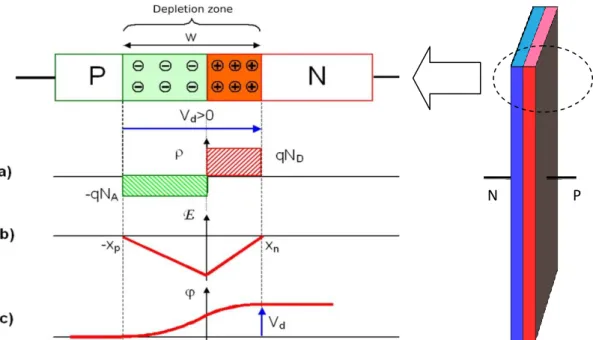
PN junctions are formed by joining n-type and p-type semiconductor materials as shown in Figure 2.3. Since the n-type region has a high electron concentration and the p-type one has a high hole concentration, electrons diffuse from the n-type side to the p-type side. Similarly, holes flow in the other side. In a PN junction, when the electrons and holes move to the other side of the junction, they leave behind exposed fixed charges on dopant atom sites. An electric field E forms between the n-type material and the p-type material and hence a "built in" potential Vbi is formed. A
"depletion region” is formed since the electric field quickly sweeps free carriers out.
Figure 2.3: Formation of a PN junction in the Schottky approximation. (a) space-charge distribution due to fixed ionized dopants; (b) electric field obtained by integration of the Poisson equation; (c) a second integration step results in the electrostatic potential
14
Even with the presence of a barrier created by the electric field, some carriers still cross the junction by diffusion. Some carriers will have a high velocity and travel in an enough net direction such that they cross the junction [2-5]. Once a majority carrier crosses the junction, it becomes a minority carrier. It will continue to diffuse away from the junction and can travel a distance on average equal to the diffusion length before it recombines and caused the “diffusion current”. In the other hand minority carriers which attain the edge of the diffusion region are swept across it by the electric field in the depletion region and this is the “drift current”. As a result In equilibrium, the net current from the PN junction is zero.
2.3 Current in diode
The diode is three dimensional but the n-type and p-type regions are assumed to be infinite sheets (Figure2.3) so the properties are just varying in one dimension. The one dimensional model greatly simplifies the equations [6].
The diode equation gives an expression for the current through a diode as a function of voltage. The operation of actual solar cells is typically treated as a modification to the basic ideal diode equation:
Id is the net current flowing through the diode, I0 is the “dark saturation current"or the
diode leakage current density in the absence of light, V is applied voltage across the terminals of the diode, q is the absolute value of electron charge.
For non ideal Diodes, the expression becomes:
Where n is the ideality factor, a number between 1 and 2 which typically increases as the current decreases [6].
15 2.4 Types of Semiconductor Junctions
Usually one can find five different types of semiconductor junctions that have application in photovoltaic solar cells, (1) Homojunction, (2) Heterojuction, (4) metal-semiconductor junctions, and (5) metal-semiconductor-electrolyte junctions.
2.4.1 Homojunction and Heterojuction
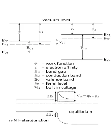
Junctions between two semiconductor materials can be classified into Homojunction; these are the PN junctions of identical semiconductors and Heterojuction. Heterojuction is formed by two different semiconducting materials with unequal band gaps. The behavior of a semiconductor junction depends crucially on the alignment of the energy bands at the interface. Semiconductor interfaces can be organized into three types of Heterojuction as shown in Figure 2.4.
To construct the energy band diagrams of a Heterojuction we use the Anderson's rule [8] called electron affinity rule. The vacuum levels of the two semiconductors on either side of the Heterojuction should be aligned (at the same energy). Once the vacuum levels are aligned it is possible to use the electron affinity and band gap values for each semiconductor to calculate the conduction band and valence band offsets. The electron affinity (χ) gives the energy difference between the lower edge of the conduction band and the vacuum level of the semiconductor. The band gap (Eg) gives the energy difference between the lower edge of the conduction band
and the upper edge of the valence band. For semiconductor alloys it may be necessary to use Vegard’s [9] law to calculate these values.
Figure2.4: The three types of semiconductor Heterojuction organized by band alignment
16
Anderson's rule allows the calculation of the band offsets of both the valence band (ΔEV) and the conduction band (ΔEc). After applying Anderson's rule and discovering
the bands' alignment at the junction, Poisson’s equation can then be used to calculate the shape of the band bending in the two semiconductors.
χ χ
Next, suppose that the band gap of semiconductor 2 is large enough that the valence band of semiconductor 1 lies at a higher energy than that of semiconductor 2. Then the valence band offset is given by:
χ χ
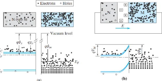
2.4.2 Metal-semiconductor contact
In particular, a large mismatch between the Fermi energy of the metal and semiconductor can result is a high-resistance rectifying contact. A proper choice of materials can give a low resistance Ohmic contact. Though for most semiconductors there is no appropriate metal available. One can creates a tunnel contact. Such contact
17
consists of a thin barrier obtained by heavily-doping the semiconductor through which carriers can readily tunnel [10]. Thin interfacial layers also affect contact formation. Most metal-semiconductor contacts are annealed or alloyed after the initial deposition of the metal in an effort to further improve the contact resistivity.
2.4.2.1 Ohmic contact
A metal-semiconductor junction results in an Ohmic contact if the Schottky barrier height is zero or negative. In such case, the carriers are free to flow in or out of the semiconductor so that there is a minimal resistance across the contact. For an n-type semiconductor, the work function of the metal must be close to or smaller than the electron affinity of the semiconductor. For a p-type semiconductor the work function of the metal must be close to or larger than the sum of the electron affinity and the band-gap energy. The work function of most metals is less than 5V and a typical electron affinity is about 4 V [10].
2.4.2.2 Tunnel contact
Such contacts do have a positive barrier at the metal-semiconductor interface, but also have a high enough doping in the semiconductor. If the width of the depletion region at the metal-semiconductor interface is very thin, on the order of 3 nm or less, carriers can readily tunnel across such barrier. The required doping density for such contact is 1019 cm-3 or higher [11].
Figure 2.6: Illustration of metal–semiconductor contact in thermal equilibrium. (a) Separated type semiconductor and metal, (b) Ideal physical contact between N-type semiconductor and metal .
(b) (b)
18 2.5 Solar cell efficiency
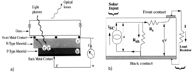
To understand the electronic behavior of a solar cell, it is useful to create a model which is electrically equivalent, and is based on discrete electrical components whose behavior is well known. An ideal solar cell may be modeled by a current source in parallel with a diode; in practice no solar cell is ideal, so a shunt resistance and a series resistance component are added to the model [4]. The resulting equivalent circuit of a solar cell is shown on the left. Also shown, on the right, is the schematic representation of a solar cell for use in circuit diagrams.
By Ohm's law, the current diverted through the shunt resistor RSH is:
Substituting these into the first equation produces the characteristic equation of a solar cell, which relates solar cell parameters to the output current and voltage:
Figure 2.7: a) Side view schematic of a solar cell showing the various layers, the process of charge separation, charge transport and, charge collection by the external contacts . b)the equivalent circuit of solar cell
19
Rs is series resistance, Rsh is shunt resistance, JL is current (current density ) due to
illumination of radiation, Joo is reverse saturation current factor, n is diode factor and
Ea activation energy of defect states.
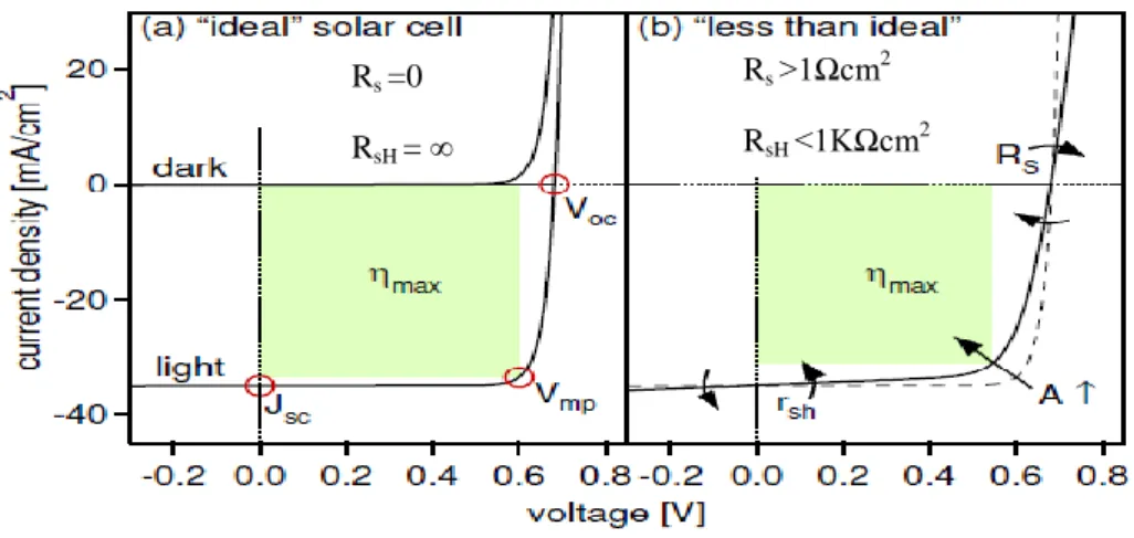
When the cell is operated at open circuit, I = 0 and the voltage across the output terminals is defined as the open-circuit voltage. Assuming the shunt resistance is high enough to neglect the final term of the characteristic equation, the open-circuit voltage Voc is [12]:
Similarly, when the cell is operated at short circuit, V = 0 and the current I through the terminals is defined as the short-circuit current. It can be shown that for a high-quality solar cell (low RS and I0, and high RSH) the short-circuit current Jsc ≈ JL .
We define the conversion efficiency of the solar cell as the fraction of incident solar power, which can convert in electrical power. In order to test the efficiency (η) of the cell, the short-circuit current (Jsc), the open circuit voltage (Voc), the maximum
voltage ( Vm), and the maximum current (Im) are to be establish:
η
Here, Pm=Im .Vm (in Watt) is maximum electrical power as illustrated in Figure 2.8, Im
and Vm values of current and voltage corresponding the maximum output power, E (in
W/m2 ) is light irradiance and S is the surface area of the solar cell.
The fill factor (FF) defines the portion of electrical power produced in solar cell in load. The fill factor is the ratio of the maximum electrical power divided by the open-circuit voltage and the short-open-circuit current
When substituting Pm the efficiency will be :
η
20
The series and shunt resistance of solar cell influence on the fill factor. Increase of shunt resistance and decrease of series resistance result in to higher fill factor and thereby to larger efficiency
2.6 Detailed Balance and Main Assumptions
In a solar cell the photovoltaic conversion in its simpler form supposes several steps as shown in Figure 2.9:
a) Solar photon transferred to the active part of the system
b) Absorption of the photons and energy transfer to the electronic system; c) Selective extraction of electrons to contacts (2 at least);
d) Channeling of e-free energy to useful load whose impedance is adjusted
Figure 2.9: several steps of photovoltaic conversion
Figure 2.8: (a) Light and dark J-V curves for an ideal solar cell; standard J-V parameters that describe performance are indicated. (b) Non-ideal behavior includes parasitic
resistances and a diode quality factor greater unity.
Rs =0
RsH =
Rs >1Ωcm2
21
The conversion efficiency of a solar cell, under "standard test conditions" (STC), was first calculated by William Shockley and Hans Queisser in 1961[13]. The modern SQ Limit calculation is a maximum efficiency of 33% for any type of single junction solar cell [14]. The original calculation by Shockley and Queisser was 30% for a silicon solar cell. Current solar cell production efficiencies vary by the band gap of the semiconductor material as shown in Figure 2.10. The following assumptions was associated with the SQ Limit that restrict its general applicability to all types of solar cells.
- One semiconductor material per solar cell. - One PN junction per solar cell.
- The sunlight is not concentrated, a "one sun" source.
- All energy is converted to heat from photons greater than the band gap
If one assumes that the total sun energy is 100% and only 33% of it is theoretically converted to electricity, Where Does The 67% of energy loss go? 47% of the solar energy gets converted to heat. 18% of the photons pass through the solar cell and 02% of energy is lost from local recombination of newly created holes and electrons [14].
Figure 2.10: Maximum theoretical efficiency (Shockley–Queisser limit) for solar cells under AM1.5 illumination without concentration
22 approaches to exceed SQ limit:
To obtain better efficiency than the SQ limit some strategies were proposed:
- Use more than one semiconductor material in a cell and/or use graded material.
- use more than one junction in a cell (tandem cell)
- use inexpensive lenses to concentrate sunlight.
- Combine a PV semiconductor with a heat based technology to harvest both forms of energy and/or use "quantum dots" to harvest some of the excess photon energy.
2.7 Light absorption
The basic concept of the photovoltaic process is also simple. When light with photon energy greater than the band gap is absorbed by a semiconductor material, free electrons and free holes are formed by optical excitation in the semiconductor.
2.7.1 The sun
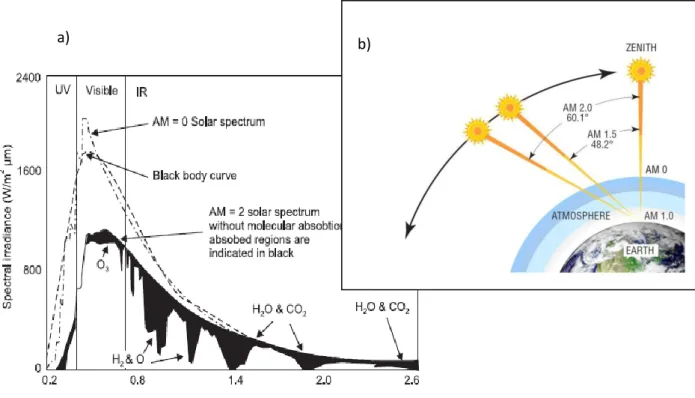
The sun, the center of our solar system, is about 149 million kilometers from our earth. The sun’s volume is about a million times the earth and its core temperature is about 15 million °C. It takes about eight minutes for light to travel from the sun to earth [15]. The sun emits a considerable power as electromagnetic radiation (4×10²³ kW) into space, burning some 1015 g/s of hydrogen in nuclear reactions and converting some 5000 t/s of matter into pure energy. The amount of solar radiation received at the top of earth's atmosphere has been measured recently to be 1.361 (kW/m²) [16]. As shown in figure 2.11, various energy losses to the solar radiation occur when it passes through the earth’s atmosphere.
A concept that characterizes the effect of a clear atmosphere on sunlight, is the ‘air mass’, equal to the relative length of the direct beam path through the atmosphere. The extraterrestrial spectrum, denoted by AM0 (air mass 0) is important for satellite applications of solar cells. At its zenith, the radiation from the sun corresponds to AM1, while AM1.5 is a typical solar spectrum on the earth’s surface on a clear day. That, with total irradiance of 1 kW/m2, is used for the calibration of solar cells and modules.
23 2.7.2 Optical Absorption in Semiconductor
In direct gap semiconductor, by shedding light on the p-type semiconductor at photon energy of Eg, the valence electrons are excited from the top of the valence
band to the bottom of the conduction band, generating holes in the valence band and an equal amount of minority carriers (electrons) in the conduction band. After electrons are injected to the conduction band, they recombine with the majority carriers (holes) to emit light within their short lifetime τr [17]. The situation is quite
different in an indirect gap semiconductor such as Si, as shown in Figure 2.12.
Figure 1.6â•… E v. k curve of a direct band gap semiconductor
Figure 2.12: direct band gap semiconductor and indirect band gap semiconductor Figure 2.11: a) Energy losses at earth atmosphere, b) Different values of AM vs. solar position
24 2.8 Solar cell generations
The majority of solar cells that exist on the market belong to the first generation of solar cells, based on silicone mono-crystalline [17]. These products are based on silicon wafers, either single-crystalline or a lower-grade multi-crystalline wafers. The production volume is growing with the focus on improving the efficiency and reducing the cost. The second generation of solar cells has the objective of reducing the production cost by using polycrystalline silicone or different semiconductors (CdTe, CuIn,.. ) thin films.
The main aim of third generation solar cell is obtaining high efficiency. To achieve such efficiency improvements, devices aim to circumvent the Shockley-Queisser limit for single band-gap devices that limits efficiencies to either 31% or 41%, depending on concentration ratio. Different methods have been proposed [18]:
a. Utilization of materials or cell structures incorporating several band gaps: Si-based multi-junction solar cells b. Modification of the photonic energy distribution prior to absorption in a solar cell: Photon energy down-conversion and Photon energy up-conversion
c. Reducing losses due to thermalization: Hot carrier solar cells and Impact ionization solar cells.
25 2.9 Thin film solar cell
2.9.1 What thin films mean
Chopra et al. [19] define a thin film as a material “created by the random nucleation and growth processes of individually condensing/reacting atomic/ionic/molecular species on a substrate. The structural, chemical, metallurgical and physical properties of such a material are powerfully dependent on a great number of deposition parameters and may also be thickness dependent. Thin films may encompass a considerable thickness range, varying from a few nanometers to tens of micrometers and thus are best defined in terms of the production processes rather than by thickness. The given definition still leaves room for a broad field of technologies to deposit the thin film (plasma, sputtering, evaporation, deposition from the liquid phase, etc.) and to tailor its electrical and morphological properties (crystalline, amorphous and intermediary forms) [20].
Thin film solar cells have several other benefits and downsides [21]
Advantages
Significantly higher temperature resistance compared to crystalline-based solar panels.
Many thin-film modules are flexible, which greatly increases the number of potential applications (e.g. curved surfaces, building-integrated photovoltaic). Better resistance against shading.
Disadvantages
Lower efficiency rates mean you need a physically larger system for the same power output.
Installation costs goes up because you need to install more solar panels. Thin film solar panels tend to degrade faster.
Silicon costs are declining and silicon-based solar panels (e.g. mono- and polycrystalline) are becoming more affordable.
26 2.9.2 Crystalline silicon thin film solar cells
The idea is to realize a thin crystalline Si film of high electronic quality similar to the classical crystalline Si on a low cost Si carrier substrate by means of epitaxial growth. The epitaxial cell approach relies on the use of a Si substrate. There are also attempts to develop thin film crystalline Si solar cell structures on non-Si substrates
2.9.3 Amorphous and microcrystalline silicon thin film solar cells
Whereas c-Si solar cells are commonly made from self-supporting slices sawn from a silicon ingot. The active silicon layers in thin-film silicon PV are deposited from the gas phase in a low-temperature process on a cheap substrate such as glass, steel or plastic [22]. Because a-Si:H can be doped efficiently p- and n-type, the cell structure is based on a Homojunction. As a result of the short carrier lifetime and the low carrier mobility collection by pure diffusion of excess carriers is not very effective. Therefore a-Si:H solar cells also include a drift zone to improve the carrier collection. As a result the structure of the solar cell device is a p-i-n-structure where an intrinsic a-Si:H layer is sandwiched between a thin n+ and p+ type layer. A typical a-Si:H based Multijunction solar cell structure is shown in Figure 2.14.
a) a)
Figure 2.14: a) Cross section of typical Multijunction solar cell based on a-Si:H. a) SiGe:H alloys,b) replacing the a-Si:H bottom cell by a microcrystalline Si solar cell
27 2.9.4 Cadmium telluride solar cells
Cadmium telluride has a direct band-gap Eg =1.45 eV, which is well within the optimum range of 1.2 eV to 1.5 eV for maximum photovoltaic energy conversion [20]. Because of the high optical absorption coefficient, a few micrometers of CdTe is sufficient to absorb all the incident sunlight [20]. When CdTe is deposited onto substrates above 449°C it condenses stoichiometrically as the stable phase in this regime [23]. These films are in general p-type with carrier concentrations of p. First Solar has reported a world record for a CdTe solar cell with a conversion efficiency of 21.4% [24]
2.9.5 Chalcopyrite
Chalcopyrites with Cu(In,Ga)(S,Se)2 are an interesting material system . it has as
a tunable band-gap (ranging from 1.01 eV for CuInSe2 to 1.68 eV for CuGaSe2 or 2.4
eV for CuGaS2) by substituting indium with gallium or selenium with sulfur, high α
(105cm-1) [13, 17], and a technology which is mature since more than 20 years Significant progress has not only been made in the basic understanding of the material properties of these devices, but also in the field of large area production of monolithically interconnected modules. The first CuInSe2 /CdS solar cell was realized
in the early 1970s at Bell Labs [25].The best result (20.4±0.6%) was achieved by Solibro [26].
28
a-Si/nc-Si CdTe CIGS
Best research-cell efficiency 13.4 ± 0.4 % LG Electronics 21.0±0.4% First Solar 20.5±0.6% Solibro Best solar module efficiency 12.2 ± 0.3 % 17.5 ± 0.7 % 17.5 ± 0.5 % Thin film market share 32% 43% 25% Advantages Mature technology Excellent for small devices Low cost manufacturing High efficiency Glass or flexible substrates Disadvantages Low efficiency High cost equipment Medium efficiency Rigid glass substrates Cadmium is highly toxic Costly traditional process
Market share expected to grow Requires less cadmium than CdTe solar cells.
2.10 Other solar cell types
2.10.1 Organic Photovoltaics OPV
Photoconductivity in some organic solids arises because the conjugated -electronic orbitals of neighboring molecules overlap sufficiently to allow charge transport by hopping. Light absorption in organic semiconductors creates short lived excitons, rather than ‘free’ carriers, as in broadband inorganic semiconductors [28]. In an organic photoconducting device, the field is supplied by the external electric bias on the electrodes. In an organic photovoltaic cell, the field is usually created at the heterojunction between two different materials, one with donor, and the other with
29
acceptor, properties. OPV has the advantages of cheapness, lightness and band-gap tenability .Their disadvantage is their poor stability and lifetime [27, 28].
2.10.2 III–V Tandem and Multijunction Cells
Solar cells with different band-gaps are stacked one on top of the other so that the cell facing the Sun has the largest band-gap. The cells cover a wide wavelength region from 300 nm to 1800 nm. This top cell absorbs all the photons at and above its band-gap energy and transmits the less energetic photons to the cells below. The next cell in the stack absorbs all the transmitted photons with energies equal to or greater than its band-gap energy, and transmits the rest downward in the stack. InGaP/GaAs/Ge, InGaP/InGaAs/Ge, AlInGaP/GaAs/Ge and AlGaAs/GaAs/Ge are candidate material combinations [27]. Multi-junction solar cells are very expensive, so they are mainly used in high performance applications such as satellites at present.
2.10.3 Dye-sensitised solar cell (DSSC)
A schematic of the components of a DSSC is shown in figure 2.14.a). At the heart of the system is a mesoporous oxide layer composed of nanometre-sized particles that have been sintered together to allow electronic conduction to take place. The material of choice has been TiO2 although alternative wide-gap oxides have also been
investigated. Attached to the surface of the nanocrystalline film is a monolayer of a sensitizer dye. Photoexcitation of the latter results in the injection of an electron into the conduction band of the oxide, generating the dye cation. The original state of the dye is subsequently restored by electron donation from the electrolyte; this step is often referred to as the regeneration reaction. The electrolyte usually comprises an iodide/triiodide redox couple dissolved in a liquid organic solvent [27, 29].
2.10.4 Quantum Well Solar Cells
The quantum well solar cell (QWSC) was proposed as a new type of multiple-band-gap, single-junction solar cell [30]. The idea is rather than using two junctions made from different semiconductors, the QWSC uses ultra-thin layers of different materials in a monolithic, two-terminal arrangement. The QWs are thin layers of a
30
second, narrower gap semiconductor between barrier layers of the host material. III–V semiconductors are normally used for both QW and host material. Typically the QWs are 60–150Å wide, separated by barriers of 50Å or more. Some 50 QWs can be placed in an i -region 0.5–1μm thick [27].
2.10.5 Concentrator photovoltaics CPV
Concentrators are optical elements that collect the Sun’s energy in a certain area and redirect it onto the solar cells. Sun light can be magnified at a range of up to 500x or 1000x which strike solar cell with efficiency of 35 % 40% [31]. Obviously the collecting optical element has to be cheaper per unit area than the solar cell, The rapid decrease of the price of silicon solar cells and the irruption of thin film cells in the market has weakened the convincing strengths of this approach. However, the interest in (CPV) has appeared, namely the fabulous potential of Multijunction cells for high efficiency under concentration [27].
31
Figure 2.15: a) simplified scheme of operation principle of ,a)organic solar cell ,b) Dye solar cell , c) Concentrator Systems, d) Quantum Well Solar Cells
a)
b)
c)
32 References of chapter 2
[1] https://ocw.tudelft.nl/wp-content/uploads/Solar-Cells-R3-CH3_Solar_cell_materials.pdf/ (03/2016)
[2] http://www.optique-ingenieur.org/en/courses/ (03/2016)
[3] A. Kitai, Principles of Solar Cells, LEDs and Diodes The role of the PN junction, John Wiley & Sons, Ltd,( 2011).
[4] S. Fonash, Solar Cell Device Physics, (1981).
[5] L. A. Kosyachenko ,Solar Cells ,Thin-Film Technologies, ISBN 978-953-307-570-9, (2011).
[6] http://pveducation.org/pvcdrom/pn-junction/ (02/2016).
[7] https://en.wikipedia.org/ (02/2016).
[8] R. L Anderson, Germanium-gallium arsenide heterojunction, IBM J. Res. Dev. 4(3), pp. 283–287 (1960).
[9] S. Adachi, Properties of Semiconductor Alloys: Group-IV, III–V and II–VI Semiconductors , John Wiley & Sons, Ltd ISBN: 978-0-470-74369-0 (2009).
[10] S. Dimitrijev, Principles of semiconductor devices, 2nd ed. Oxford University Press (2012).
[11] http://ecee.colorado.edu/~bart/book/book/chapter3 (01/2016).
[12] S. R. Kodigala, Thin Film Solar Cells from Earth Abundant Materials, Elsevier Inc, ISBN: 978-0-12-394429-0, (2014).
[13] W.Shockley , H.J.Queisser , 1961 Detailed balance limit of efficiency of p-n junction solar cells J. Appl. Phys. 32, 510-519,(1961).
[14] http://solarcellcentral.com/limits (06/2015)
[15] G. Kopp, G. J. Lean , A new, lower value of total solar irradiance: Evidence and climate significance, Geophys. Res. Lett. 38: L01706, (2011).
33
[17] K. Ito, Copper zinc tin sulphide-based thin film solar, John Wiley & Sons, Ltd , ISBN 978-1-118-43787-2 (2015).
[18] A. M. Acevedo, Solar Cells - Research and Application Perspectives (2013), ISBN 978-953-51-1003-3, (2013).
[19] K. L. Chopra, P. D. Paulson and V. Dutta, Thin-film solar cells: an overview, Progress in Photovoltaics: Research and Applications, 12, 69–92 (2004).
[20] J. Poortmans and V. Arkhipov , Thin film solar cells : fabrication, characterization, and applications, J.Wiley & Sons Ltd (2006).
[21] http://energyinformative.org/best-thin-film-solar-panels-amorphous-cadmium-telluride-cigs/ (01/2016)
[22] G. J. Conibeer, A. Willoughby, Solar Cell Materials: Developing Technologies John Wiley & Sons, Ltd (2014).
[23] K. Zanio, Cadmium Telluride: Material Preparation, Physics, Defects and Application in Semiconductors and Semimetals, vol. 13. Academic Press, New York (1978).
[24] First Solar Press Release, August 5, (2014)
[25] S.Wagner, J.L.Shay, P.Migliorato & H.M.Kasper, Applied Physics Letters, 25, 434 (1974).
[26] M. A. Green, K. Emery , Y. Hishikawa , W.Warta & E. D. Dunlop, Solar cell efficiency tables (Version 45) Prog. Photovolt: Res. Appl. 23:1–9 (2015).
[27] M.D. Archer & M. A.Green, Clean electricity from photovoltaics, 2nd Edition, Imperial College Press (2015).
[28] Q. Qiao & K. Iniewski, Organic Solar Cells, CRC Press T & F Group, (2015)
[29] L. A. Kosyachenko, Solar Cells – Dye-Sensitized Devices, InTech (2011)
[30] M.Green, Third Generation Photovoltaics: Advanced Solar Energy Conversion, Springer Series in Photonics, Springer,(2005).
Chapter
3
34 Chapter 3: Graded solar cell
3.1 An alloy and a compound
According to S. Adachi [1] an alloy is formed from a physical mixture of two or more substances, while a compound is formed from a chemical reaction. An alloy crystal is sometimes called a mixed crystal or a solid solution. For example, GaAs is a compound consisting of (Ga) atoms bonded to (As) atoms, it is not an alloy. AlyGa1-yAs is an alloy compound consisting of AlAs and GaAs with a mole ratio of
y:(1- y). The bonds in GaAs and AlAs are not adequately described by any of these extreme types, but have characteristics middle to those usually associated with the covalent and ionic terms. The bonds in diamond, C-C, can be described by the covalent bond term only. It is an elemental semiconductor, not a compound semiconductor. Similarly, Si and Ge are elemental semiconductors. An alloy with two components is called a binary alloy; one with three is a ternary alloy; one with four is a quaternary alloy; one with five is a pentanary alloy. The resulting alloy substance usually has properties significantly different from those of its components.
3.2 Uniform or graded absorber
In uniform layers, the driving forces for electrical current are the electrostatic potential gradient ∇Φ (drift current) and the concentration gradients ∇n and ∇p (diffusion current). When grading is present, additional driving terms should be added: the gradient of the electron affinity ∇χ, the gradient of the band gap ∇Eg, and the gradients of the effective density of states in the conduction and valence bands: ∇(log NC) and ∇(log NV). Also, the electron and hole continuity equations are modified by the presence of a mobility gradient ∇μn or ∇μp (eq (3.1)), and the Poisson equation is modified by a gradient ∇ε in dielectric constant (eq.(3.2)). These modified equations have been described in the literature [2,3] and are implemented and solved in SCAPS [3]. Φ Φ
35
When gradients in electron affinity χ or band gap Eg are present, this formalism is extended by adding the ‘band potentials ’ n and p to the electrostatic potential Φ[3]
The graded material can be viewed as a series of sub-layers or sheets . Each layer is divided in SCAPS in a number (typically 100 or larger) of sub-layers or sheets, The
effective electrostatic potentials Φn and Φp evaluated (in SCAPS) at each sub-layer or sheet are given by equations (3.3) and (3.4), (n for electron, p for holes ) [4] :
(the factor kT/q or KT is needed, all 3 terms must have the same dimension of voltage,
Eg is an energy, Eg/q is a voltage) .Here NC0 and NV0 are arbitrarily chosen reference values for the density of states NC in the conduction band and NV in the valence band.
3.3. CZTSSe solar cell
3.3.1 Overview
The increase of energy prices has increased the attention for renewable energies significantly. This is reflected in the large number of theoretical and experimental papers in this area, in particular solar cells. Thin-film solar cells technology still offers the possibility of reducing the manufacturing costs. However, Most of the materials used in the production of thin film absorber contain either rare or toxic elements. Nowadays, the quaternary p-type semiconductors Cu2ZnSnSe4(CZTSe),
Cu2ZnSnS4(CZTS) and their alloys Cu2ZnSn(S1-ySey )4 (CZTSSe) with direct band
gab between 0.7 and 1.5 eV has particularly attracted attentions[5.6]. Those materials are derived from CuInGaSe2 (CIGS) and keep its noticeable photovoltaic properties,
but also contains earth abundant and safe elements like Zn and Sn . The pre-factor of absorption coefficient for the CZTSSe thin film is large enough (>104cm-1), in other
36
word the absorber of just micron thickness is able to absorb sunlight sufficiently, and without any damaging effects on photocurrents.
Despite The discovery that a CZTS thin film has an optimum direct band gap of 1.45eV for solar cells was made in1988 in the laboratory of Shinshu University [7], the efficiency of CZTSSe solar cells remains under that of devices with absorbers produced from older materials such as CIGS (η % 20.4%), CdTe (η % 19.6%) and GaAs (η % 28.8%) [8] .The current highest photoelectric conversion efficiency of CZTSe and CZTS based solar cells is 12.6% [ 9] and 8.5% [10] respectively this efficiency is very low compared with its theoretical limit ( > 32 %), according to Shockley-Queisser photo balance calculations [11]. To increases the conversion efficiency of CZTSSe solar cell, several optimization techniques have been proposed.
Usually, in uniform solar cell, the band gap energy Eg of the absorber material is
optimized by the well known exchange between high current for low Eg and high
voltage for high Eg. To achieve further increase in the efficiency, grading of the band
gap Eg(x) and most other materials properties in the cell thickness direction (x) can be
involved. This can be achieved by using a compositional graded absorber. The idea is to increase the short circuit current Jsc while maintaining the open circuit voltage by
realizing a well suited band gap profile Eg(x). K. Woo & all reports that high Jsc and
less loss of Voc are attributed to the effect of band gap grading induced by (Se)
grading in the CZTSSe absorber layer [12].
3.3.2 Material properties
3.3.2.1 The Crystal Structure of CZTS
Quaternary compounds of the Adamantine family can be represented by the general Formula ). The most important are the compounds (N=2). They crystallize in the kesterite- or stannite-type structure which belong to the tetragonal crystal system, as well as in the kesterite or wurtz-stannite-type structure [13]. Schematic of the cross-substitution steps required to form (I2 –II–IV–VI 4) compounds is shown in Figure 3.1. The formation of stoichiometric
multi-component semiconductors can be considered as a sequential process involving a series of cation mutations (cross-substitutions) in which the overall valence state is maintained and the compound remains charge neutral [14]. For example, two 3 + ions [III] have an equivalent charge to one 2 + and one 4 + ion [II–IV] or one 1 + and one