HAL Id: hal-02096904
https://hal.archives-ouvertes.fr/hal-02096904
Submitted on 11 Apr 2019HAL is a multi-disciplinary open access archive for the deposit and dissemination of sci-entific research documents, whether they are pub-lished or not. The documents may come from teaching and research institutions in France or abroad, or from public or private research centers.
L’archive ouverte pluridisciplinaire HAL, est destinée au dépôt et à la diffusion de documents scientifiques de niveau recherche, publiés ou non, émanant des établissements d’enseignement et de recherche français ou étrangers, des laboratoires publics ou privés.
Multi-functional metasurfaces based on direct
nano-imprint of Titania sol gels coatings
Simona Checcucci, Thomas Bottein, Massimo Gurioli, Luc Favre, David
Grosso, Marco Abbarchi
To cite this version:
Simona Checcucci, Thomas Bottein, Massimo Gurioli, Luc Favre, David Grosso, et al.. Multi-functional metasurfaces based on direct nano-imprint of Titania sol gels coatings. Advanced Optical Materials, Wiley, 2019, pp.1801406. �10.1002/adom.201801406�. �hal-02096904�
Multi-functional metasurfaces based on direct nano-imprint of
Titania sol gels coatings
Simona Checcucci1,2,3, Thomas Bottein1, Massimo Gurioli1,⊥, Luc Favre1, David Grosso1,* and
Marco Abbarchi1,**.
Dr. S. Checcucci, Dr. T. Bottein, Prof. M. Gurioli, Prof. L. Favre, Prof. D. Grosso, Prof. M. Abbarchi
CNRS, Aix-Marseille University, UMR 7334, IM2NP, F-13397, Marseilles, France Dr. S. Checcucci,
European Laboratory for Nonlinear Spectroscopy (LENS), 50019 Sesto Fiorentino, Italy. Dr. S. Checcucci,
Dipartimento di Fisica ed Astronomia, Universitá degli Studi di Firenze, 50019 Sesto Fiorentino, Italy
* Corresponding author: [email protected] ** Corresponding author: [email protected]
⊥Permanent address: Dipartimento di Fisica ed Astronomia, Universitá degli Studi di Firenze,
50019 Sesto Fiorentino, Italy
Keywords: Dip Coating, Nano-Imprint, Mie Resonators, Dynamic Structural Colour, Sensing
Abstract
Dielectric Mie resonators are taking momentum in the last years thanks to their peculiar properties in light management at visible and near-infrared frequencies. However, their full exploitation demands for cheap materials and versatile fabrication methods, extendible over large surfaces and potentially C-MOS compatible. Here, a sol-gel deposition and nano-imprint lithography method is used to obtain Titania-based Mie resonators over large areas (several mm2), showing that this platform can potentially be exploited for light management with
different devices. First, it is demonstrated their use for structural colours and efficient band pass filters covering the visible spectrum. Then, exploiting sharp Fano resonances in reflection, their potential for refractive index sensing is addressed obtaining a figure of merit of ~20. Finally, when placing the resonators on porous silica, a large and reversible colour tuning can be produced as a result of water adsorption within the substrate porosity. These results open the path to Titania sub-micrometric structures for applications as a multi-functional metamaterial for smart windows, displays and all-optical sensing.
1. Introduction
Dielectric metasurfaces composed of high-permittivity and sub-micrometric elements1,2,3
(dielectric Mie resonators) are challenging plasmonic structures4,5,6 for light manipulation at
visible and near-infrared frequencies thanks to their peculiar performances associated to reduced ohmic losses and a higher compatibility with electronic devices. Anti-reflection coatings,7 mirrors,8,9 lenses,10 polarisers,11 wave-front shaping,12,13,14 sensing,15,16 and non-linear
phenomena17,18,19,20 are few examples demonstrating the strength of this approach for light
management with sub-wavelength dielectric-structures. However, with a few exceptions based on colloidal assembly,21,22,23 hydro-thermal growth,20 solid state dewetting24,25,26,27,28,29,30
fabrication methods involving several steps (such as e-beam lithography and reactive ion etching). Top-down fabrication approaches limit the full exploitation of Mie resonators for un-expensive devices and broad areas production. In particular, given the rapidly rising interest in structural colouring and light filtering with dielectric metasurfaces32,33,34,35,36,37,38,39,40,41 a versatile and scalable method is highly desirable to
overcome the gap separating mere proof of principles and industrial applications. In this framework, a major step forward would be the development of fabrication techniques fully compatible with back-end processing of C-MOS circuitry (e.g. keeping the maximal processing temperature below ~450 oC) or more generally, on electronic devices such as
LEDs and photovoltaic panels.
So far, most studies on Mie resonators are based on Si or Ge materials, due to both their very large index of refraction and the possibility to exploit the well-developed nanofabrication approaches of nano-electronics and nano-photonics. Among other materials, TiO2 (Titania) is
recently attracting growing interest42,43,44,45,46,47 for its transparency up to near-UV frequencies
and its relatively high refractive index. Indeed, TiO2–based Mie resonators systems can
potentially outperform conventional Si- and Ge-based dielectric metasurfaces which suffer from larger absorption at short wavelength48,49 (e.g. at 450 nm: n
TiO2 = 2.55, kTiO2 = 1.2·10−5; nSi
= 4.5, kSi = 0.13; nGe = 4, and kGe = 2.24). A quite unique peculiarity of Titania is the tuneable
porosity (adjustable by modifying the sol-gel fabrication process) and therefore permeability to liquids and gas. In addition to this, Titania is an abundant, cheap, non-toxic, photo-catalytic, mechanically strong and chemically stable material, featuring a relatively low mass density (~3.8 g/cm3 in the anatase form against ~5 g/cm3 for MoS
2). These features make
Titania an ideal metamaterials providing several functions (e.g. tuneable structural colour, sensing small changes in the environment), for a novel photonic platform in view multi-functional devices.
In spite of several reports on Titania-based Mie resonators, the implementation of sub-micrometric structures with conventional methods (e.g. e-beam or optical lithography and reactive ion etching) remains limited to small size and hardily scalable. Very recently, we reported the use of sol-gel chemistry combined with aerosol-spray processing to elaborate Titania sub-micron spheres31 and investigate their scattering properties on various substrates.
This chemistry was also coupled to nano-imprint lithography (soft-NIL) process to form Titania-based Mie resonator arrays.46,47 This approach has been successfully used for
color-printing with aluminum-based structures for plasmonic50,51 and, more recently, perovskite
nanostructures for light emission.52 Developing a method for large-scale fabrication of Titania
on ultra-low per-area mass supports (such as aerogels), would potentially render this material a competitive candidate for light-sails to be employed in future space exploration.53,59
In the present communication, exploiting soft-NIL on Titania xerogels, we show that tailored dielectric metasurfaces can be extended over mm2 thus increasing of more than three order of
magnitude the size of the patterned surface, also with squared pillars three times smaller with respect to our previous report.46 In order to highlight the versatility of porous Titania
Mie-resonators as a platform for photonic devices, we focus on four different applications. 1) A fine size tuning of the resonant elements constituting the dielectric arrays provides neat structural diffusive colors, covering the full visible spectrum. 2) Tuneable sharp band-pass filters (up to ~40 dB rejection ratio) when impinged by light channeled in the glass slide on which the arrays are printed. 3) Gas or liquid sensors by exploiting sharp Fano resonances arising from the interference between sharp grating modes and the broad-band reflection. 4) Dynamic structural colour change by coupling the resonators onto a highly porous hydrophilic silica layer deposited on bulk silicon. In all these applications we demonstrated the relevant achievements in the main figure of merits.
2. Results
Arrays of TiO2 sub-micrometric squared pillars are obtained via soft-NIL as follows; further
details are provided in the devoted Experimental Section. We fabricated the master by e-beam lithography and reactive ion etching on a bulk silicon wafer. It contains 9 arrays each of 1 mm2 of 150 nm wide trenches milled with variable pitch (p = 380, 400, 420, 440, 460, 480,
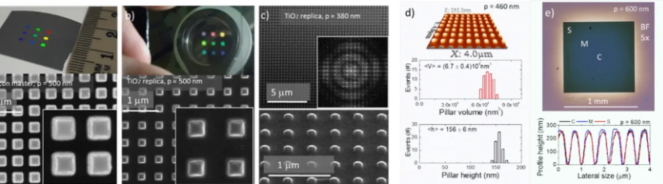
500, 550 and 600 nm) in a squared geometry (Figure1 a). We then obtained a hard polydimethylsiloxane (PDMS) mould from the master and we could use it ad libitum to replicate the photonic systems on freshly deposited sol-gel Titania. Indeed we used moulds dozen of times over several months, without damages. Their lifetimes were not investigated in this work. The Titania replicas are extremely regular as accounted for by scanning electron microscopy (SEM) and atomic force microscopy (AFM) investigations, showing fluctuations of the structural parameters of a few % (Figure 1 b-e). An extensive analysis of these morphological images confirmed a coherent replication across the arrays (Figure 1 e).
We investigated the light scattering from the dielectric arrays exploring their possible use for structural colour in conventional diffusion (e.g. for ink-free colour printing and anti-counterfeiting of banknotes). A tungsten white lamp was used for dark-field (DF) illumination in an optical microscope (the scheme of the illumination/collection geometry and of the lamp spectrum are shown in Figure 2 a and b, respectively). In Figure 2 c we report the dark-field back-scattering spectra; note that the spectra are non-normalized to the white tungsten lamp spectrum, nor background subtracted). In these measurements we used an objective lens with 20x magnification and numerical aperture NA = 0.4 determining a maximum acceptance angle of ~23 degrees.
The data show the onset of sharp resonances red-shifting and increasing in number with increasing pitch size (Figure 2 c). In literature and generally speaking, the resonances in different kind of Mie resonators are attributed to multipolar modes,31,44,45,46,66 even if this
attribution is well assessed only for spherical particles.31,54 Following this picture and
comparing small objects (p < 460 nm, having base size smaller than ~250 nm) with Titania Mie resonators featuring similar size and shape,44,45 we attribute the longer-wavelength
resonance to the magnetic dipolar mode and the second one to the electric dipolar mode. For larger pillars, the scattering spectrum becomes more complicate and a clear discrimination between the different resonances is not possible owing to the onset of higher order modes. The two samples with the largest pitches (p = 550 and 600 nm) with larger pillars accommodating several Mie resonances show a bandwidth comparable to that of the white tungsten lamp. Overall, the nine arrays cover the visible spectrum from blue to orange (Figure 2 d). Note also that a weak spurious and featureless scattering contribution is visible in the spectrum of the small pitches (the broad band peaked at ~580 nm), due to their rather low Mie-scattering in the visible.
We now address the light filtering from the dielectric arrays exploring their scattering properties for applications in displays. Exploiting the glass slide supporting the arrays we channelled the light from a white LED in the slab and we detect the scattering in air of the guided slab modes out-coupled by the Titania arrays (Figure 3 a and b). With a smart-phone camera, we took images of the pillars arrays showing marked structural colours both in the front and back sides (Figure 3 c). In Figure 3 d we report the scattering spectra from the top part (front side scattering) in a semi-logarithmic scale, in order to highlight the sharp pass band operated on the LED light (the spectra are not normalized to the LED light, nor background-subtracted). For the largest pitches (p > 500 nm) we observe a strong light
rejection out of the pass band (rejection up to 37 dB for p = 600 nm). On the contrary, light scattering from the smaller pitches (p < 440 nm) was not detectable in this illumination/collection geometry. The data show that the central frequency and, possibly, the bandwidth, can be controlled by design of the array.
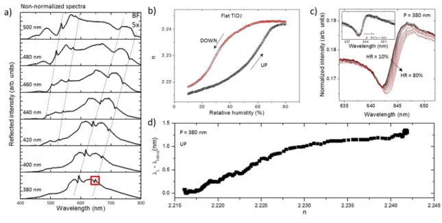
As stressed in the introduction, the use of sol-gel chemistry allowed us to have slightly porous Titania, leading to several possible uses, obviously including the sensing via small changes of the refractive index by any analyte in the pores. As proof of principle of the sensor, we used water infiltration of the Titania matrix composing the pillars and detected the reflection with a conventional bright field illumination geometry. In this case, we used a tungsten lamp light in illumination/detection configuration with a 5x objective lens. In this configuration the collected light is dominated by the reflection from the arrays (Figure 4 a) integrated over the numerical aperture of the optics (NA = 0.2 corresponding to a maximum acceptance angle of about 11 degrees). The spectra are dominated by broad bands red-shifting with increasing pillars size. Note also that relevant spectral differences can be found in different scattering geometry (Figure 2-4), due to the peculiar angular patterns of different Mie modes. In addition to this, the spectra show narrow resonances which line-shape can be either a Lorentzian or a Fano-like dispersive profile64 depending on their relative intensity with respect
to the broad-band reflection. These sharp spectral features are characteristic of a 2D high-index contrast grating and arise from interference of light due to the ordering of the Mie resonators in a two dimensional photonic crystals. The Fano profiles spring form constructive and destructive interference of the sharp grating resonances with the reflection, as commonly observed in a plethora of systems, including dielectric and plasmonic ordered structures.55,56
Fano line-shapes, characterized by a dispersive-like profile, are suitable for detecting small spectral shifts induced by refractive index changes. Exploiting the nano-porosity of the dense Titania composing the pillars (estimated around 8%vol), we induced a slight change in their
refractive index by varying the relative humidity (RH%) of the surrounding atmosphere from 10% to 80%. These changes are measured by environmental ellipsometry on the flat Titania film nearby the arrays. Adsorption and desorption of water within the pores follow a different kinetics, which is reflected in the typical hysteresis cycle in the measured refractive index on the 2D, flat Titania layer nearby the arrays (Figure 4 b).57 The study of the hysteresis can lead
to get insights into the complex dynamics of water in the Titania nano-pores, which is largely outside the scope of the paper. In view of applications we bypassed the hysteresis resetting the system at the initial conditions (no water) by heating the device at 200 oC for 10 minutes;
with this simple protocol we did measure the same variation of refractive index in each humidity cycle (not shown) guaranteeing the fidelity of the sensor. From this analysis we can also deduce a broad distribution of pore size with an average value centred at about 2.5 ± 0.5 nm.
As a last example of possible use of this metasurface platform, we addressed the dynamic colour change by modulating the refractive index of porous silica underneath the Titania arrays. We printed the dense Titania pillars (p = 1500 nm) atop a mesoporous silica layer (~650 nm thick, pore size ~7 nm, porosity estimated around 37%vol) deposited via sol-gel on a
silicon substrate (a scheme of the sample structure is shown in the inset of Figure 5 a). Then, as in the previous case, we infiltrated the pore with water by exposing the samples in atmosphere with controlled humidity. During any humidity cycle, we found that the refractive index variations were dominated by the water infiltration of silica rather than of TiO2 (Δn(TiOn(TiO2)~0.025, Δn(TiOn(SiO2)~0.11, Figure 5 a). Note also that, in the present case, the
ascribed this effect to the higher annealing temperature applied to consolidate the sol-gel bi-layers after NIL.
In Figure 5 b we report the experimental results; the spectra are not normalized to the white tungsten lamp used for illumination. By following the spectral shift of the main resonance measured in dark-field geometry, we observed an overall red-shift of about 100 nm when increasing humidity from 0% to 80%. In Figure 5c we show the spectra for a full humidity cycle in a colour-intensity map, the data show a bleaching of the scattering for RH > 80% owing to water condensation. The colour-change dynamics is also reported in Figure 5 on the CIE gamut, showing a large and reversible behaviour from yellow-green up to orange-red. As a consequence of the large broadening of the resonances, in this set of data, the hysteresis cycle is not visible.
3. Discussion
We fabricated sub-wavelength dielectric structures on mm-scales by using Titania, a material having a relatively high refractive index and high transparency up to near-UV frequencies. This makes Titania a promising photonic platform for manipulating GaN-based LED light filling the gap of use of dielectric Mie resonators to frequencies not attainable by Si and Ge owing to their larger extinction coefficient. In addition, our method is implemented at relatively low temperature (~450 oC, but lower values are in principle possible), potentially
rendering it compatible with back-end processing of C-MOS circuitry58 with the additional
advantage of relaxing the need of cumbersome fabrication steps (e.g. a device can be finalized in less than one hour in a laboratory).
Our devices can be exploited for several uses accounting for the multi-functionality of Titania-based metasurfaces. Neat structural colours spring from scattering by multipolar Mie modes formed within the dense Titania pillars, in analogy to what was found in similar systems.9,10,11,12,13,14,15,16 Choosing a convenient illumination geometry, where the light of a
white LED is coupled within the glass slide, only the fundamental modes of the Mie resonators are illuminated and can out-couple the light from the slab. This is due to the larger coupling of these resonances with the substrate with respect to higher order multi-polar modes that are more strongly confined within the pillars32,33,34,35,36,37,38,39,40,41 and do not appear in the
spectra. This property provides sharp band-pass filters potentially important for the use of these devices as ink-free colours and displays, although in this case a large dynamic tuning of the structural colour is not possible.
In back scattering geometry at normal incidence we observe sharp Fano resonances59 due to
the ordering of the Mie resonators array. Exploiting this sharp spectral line together with the porosity of sol-gel materials, we show that our structures can be suitable for refractive index sensing. We obtain a figure of merit of about 20 which is not very far from what found in the plasmonic counterpart.60,61 Our system was not optimized for efficient sensing and better
performances could be in principle obtained by using a different excitation/collection configuration or changing the unit cell geometry (see for instance reference [15] where a FOM of ~100 was demonstrated). However, the important point here is that the “sensing” occurs within the volume of the Mie resonators, where the water is adsorbed and the intensity of the electromagnetic field is larger.21,51 This observation opens up the possibility of
functionalizing the sol-gel with chemical compounds in order to detect specific substances present in the atmosphere or in solution as demonstrated for other sol-gel-based systems.62
This option is not readily available for conventional Si- and Ge-based Mie resonators which exploitation in sensing or enhanced Raman scattering requires more complex device
geometries (such as Mie resonators molecules) where the hot-spots of the electromagnetic field lie outside the pillars.
A large, dynamic and reversible colour change can be obtained when placing the Titania pillars on porous silica and exploiting its large refractive index change (Δn(TiOn of about 0.11) upon water uptake. The spectral shift of about 100 nm exceeds of about two times what was previously reported on active tuning mechanisms in similar systems63,64,65 and is obtained with
a much simpler device. As a first approximation, such a large shift can be simply ascribed to an interference effect springing from the refractive index changes in the porous medium leading to a different illumination of the scatterers. A smaller effect may spring from the coupling of the Mie modes within the substrate.66 Such a device represents an important
example of the flexibility and strength of the sol-gel/NIL approach in coupling different materials featuring different physical properties and giving access to novel functions.
4. Conclusion
In conclusion, we implemented the fabrication over large area of arrays of Mie resonators based on Titania with a high-throughput and low temperature method, combining bottom-up assembly via sol-gel deposition and top-down nano-imprint lithography. We presented several possible applications of our platform, such as structural colours for displays, refractive index sensing and dynamic colour change. The strength of this approach relies in the possibility to scale it up to larger surfaces, on arbitrary substrates (e.g, semiconductor, ceramic, metal) eventually exhibiting a curvature. It can be extended to most metal oxides and other advanced functionalities are at hand.
In perspective several points can be stressed. We already showed the possibility to fabricate our photonic structures directly on highly porous silica (aerogel layer) having low-index and low weight. Although in the present case we used meso-porous silica (porosity ~37%vol, mass
density 1.7 g/cm3), sol-gel process can also be used to form layers of MgF
2 featuring a
porosity of 80%, thus providing a very low refractive index (~1.08) and mass density (~0.6 g/ cm3).67 This is highly desirable when the criteria of choice of an efficient photonic structure
include a low per-area mass, such as the light-sails68,69 for the IKAROS70 mission
(Interplanetary Kite-craft Accelerated by Radiation of the Sun) and the Starshot Breakthrough Initiative50 established in 2010 and 2016 respectively. All these features and perspectives
render our process appealing for scaling-up and soft-NIL has certainly this potential. Finally, in this work we only addressed the simple case of squared pillars. However, the high fidelity in the replication over mm-scales and the high lateral resolution (the smaller objects have a side of about 150 nm) allow, in principle, the implementation of advanced devices made of unit cells having sharp features and more complex geometries. This opens the possibility to use soft-NIL for the production of large scale metasurfaces with more exotic optical properties and advanced functionalities.
5. Experimental Section. 5.1. Soft-NIL
Masters are fabricated via e-beam lithography and reactive ion etching on a silicon wafer. We realized samples with 9 arrays of squared pillars of height 500 nm, gap (distance between two structures) of 150 nm and pitch varying between 380 and 600 nm. We rendered hydrophobic the master surface by grafting with a fluorinated precursor. To fabricate the mould, an h-PDMS blend (h-h-PDMS from Gelest Inc) was directly poured on the hydrophobized master and partially cured for 10 mins at 50 °C then a thick PDMS buffer layer (RTV615 from Momentive) was added and the stack annealed at 50 °C for 12 hours then at 70 °C for 2 hours.
We made TiO2 replicas by using a well-established protocol:46,47 a TiO2 xerogel is first
deposited on glass by dip-coating in controlled environment (22 °C, relative humidity RH = 20%) using an ACEdip equipment from SolGelWay then placed in a specially designed chamber with controlled humidity (RH = 70%). After allowing the xerogel to equilibrate with the atmosphere for 1 min, we put the mould (first degassed under primary vacuum <10 mbar, for 10 min) into contact without any additional pressure on the freshly deposited sol-gel layer. Finally, after 1 min, the assembly (mould and substrate) is annealed at 70 °C for 5 min and unmoulded. The TiO2 replica was then annealed at 450 °C for 10 min (sample of Figure
1-4) or at 500 °C for 10 min (sample of Figure 5). In this latter case the sample was obtained from a different silicon master etched by focused ion beam in arrays of 15 x 15 m2.
We prepared sol-gel initial solutions from TiCl4, Pluronic F127 (Poyethylene
oxide-Polypropylene oxide triblock copolymer), deionized water, absolute ethanol (EtOH). TiO2
precursor solution is composed of 1 TiCl4; 40 EtOH; 7 H2O; 2.10-4 F127 molar ratios.
Solutions were stirred 24 hours at room temperature prior to use.
Characterization:
We characterized the sample morphology by scanning electron microscopy (SEM, Dual-beam FIB HELIOS 600 nanolab), atomic force microscopy (AFM, PSIA XE-100 AFM) in non-contact mode and the sample optical properties by ellipsometry (Woollam M2000V), optical microscopy (LEICA DMI5000 M), confocal spectroscopic microscopy (custom made) and angle resolved reflectance measured with a spectro-polarimetric goniometer (Light Tec).
5.2. Ellipsometry. We measured the refractive index dispersion and thickness of the TiO2
and SiO2 sol-gel coatings on flat zones of the samples, near the imprinted areas, using a
spectroscopic ellipsometry system. The environmental ellipsometric porosimetry investigation was carried out using the spectroscopic ellipsometry equipment combined with an atmospheric control chamber. We then selected deionized water as the adsorbate. The volume of adsorbed (and capillary condensed) water into the pores was followed through a time resolved measurement of the refractive index variation as a function of P/P0. Then we
measured the final volume of adsorbed water from the refractive index using the Cauchy models and the Bruggeman effective medium approximation (J. A. Woollam CompleteEASE software). We estimated the pore size distribution using a modified Kelvin’s equation for spherical pores. The structural investigation of the nanoimprinted samples was performed by AFM and high-resolution SEM.
5.3. Diffusion spectroscopy. All the presented spectra were collected using a custom made,
inverted optical bright- and dark-field microscope mounting 5x and 20x magnification objective lenses (numerical aperture NA = 0.2 and 0.4 respectively) coupled with a spectrometer and Si-based CCD linear array (Flame-T-VIS-NIR by Ocean Optics) through an optical fibre (Ocean Optics multimode fibre, VIS-NIR, core diameter 200 mm). We studied reflection and diffusion from the sample under white light illumination (OSL2 Thorlabs or a commercial white LED).
5.4 Humidity tuning set-up. The sample was placed inside a custom made chamber
surrounding the microscope objective. The relative humidity inside the chamber was driven by a flux-control set-up (ACE flow by Solgelway) and does not depend on the surrounding environment. We used an electronically controlled ramp to set the humidity inside the chamber while diffusion spectra from the sample are acquired. Before each set of measurement the relative humidity was set at RH% = 0%, in order to purge the chamber and
the sample form the ambient humidity. Furthermore, before each humidity-cycle, weheated the samples for 10 min at 250 °C in order to remove adsorbed pollutants and obtain reproducible refractive index shift with humidity variation.
Acknowledgements
This project has received funding from the European Union Horizon 2020 research and innovation programme under grant agreement no. 654148 Laserlab-Europe. S.C. acknowledges the COST action (EU COST Action MP1403) for supporting her permanence at the IM2NP institute of Marseilles. M. G. acknowledges the CNRS (France) for supporting his permanence at the IM2NP institute of Marseilles. We also acknowledge the Projects PRCI network ULYSSES (ANR-15-CE24-0027-01) funded by the French ANR agency, the LASER-LAB Europe project ARES financed by the EU, the SATT-Sud Est Project PROMETHEUS, the funding by A*MIDEX (reference. ANR- 11-IDEX-0001-02). The authors thank the Nanotecmat Platform of the IM2NP Institute of Marseille, Dr. Frédéric Bedu and Dr. Igor Ozerov (Aix-Marseille University, CNRS, CINaM) the PLANETE CT PACA clean-room facility, the CP2M and CINaM microscopy centers of Aix-Marseille University.
Received: ((will be filled in by the editorial staff)) Revised: ((will be filled in by the editorial staff)) Published online: ((will be filled in by the editorial staff))
1 S Jahani, Z. Jacob Nat. Nano. 2016, 11, 23. 2 I. Staude, J. Schilling, Nat. Phot. 2017, 11, 274.
3 S. Kruk, Y. Kivshar, ACS Phot. 2017, 4, 2638
4 K. D. Gramotnev, S. I. Bozhevolnyi, Nat. Phot. 2010, 4, 83. 5 H. A. Atwater, A. Polman, Nat. Mat. 2010, 9, 205.
6 N. Meinzer, W. L. Barnes, I. R. Hooper, Nat. Phot. 2014, 8, 889.
7 Spinelli, P., M. A. Verschuuren, and A. Polman, Nat. Comm. 2012, 3, 692.
8 P. Moitra, B. A. Slovick, Y. Z. Gang, S. Krishnamurthy, J. Valentine Appl. Phys. Lett. 2014,
104, 171102.
9 A. Arbabi, E. Arbabi, Y. Horie, S. M. Kamali, A. Faraon, Nat. Phot. 2017, 11, 415.
10 M. Khorasaninejad, W. T. Chen, R. C. Devlin, J. Oh, A. Y. Zhu, F. Capasso, Science 2016,
352, 1190.
11 Y. Yang, W. Wang, P. Moitra, I. I. Kravchenko, D. P. Briggs, J. Valentine, Nano Lett. 2014,
14, 1394.
12 D. Lin, P. Fan, E. Hasman, M. L. Brongersma Science, 2014, 345, 298.
13 E. Arbabi, A. Arbabi, S. M. Kamali, Y. Horie, A. Faraon Optica, 2017, 4, 625.
14 E. Maguid, I. Yulevich, M. Yannai, V. Kleiner, M. L. Brongersma, E. Hasman, Light Sci.
Appl. 2017, 6, e17027.
15 Y. Yang, I. I. Kravchenko, D. P. Briggs, J. Valentine, Nat. Comm. 2014, 5, 5753
16 A. Titt, A. Leitis, M. Liu, F. Yesilkoy, D.-Y. Choi, D. N. Neshev, Y. S. Kivshar, H. Altug,
Science 2018, 360, 1105
17 Y. Yang, W. Wang, A. Boulesbaa, I. I. Kravchenko, D. P. Briggs, A. Puretzky, D.
Geohegan, J. Valentine, Nano Lett. 2015, 15, 7388.
18 S. Liu, M.B. Sinclair, S. Saravi, G. A. Keeler, Y. Yang, J. Reno, G. M. Peake, F. Setzpfandt,
I. Staude, T. Pertsch, I. Brener, Nano Lett. 2016, 16, 5426.
19 L. Carletti, A. Locatelli, D. Neshev, C. De Angelis, ACS Phot. 2016, 3, 1500. 20 F. Timpu, A. Sergeyev, N. R. Hendricks, R. Grange ACS Phot. 2016, 4, 76
21 R. Fenollosa, F. Meseguer and M. Tymczenko, Adv. Mat. 2008, 20, 95.
22 M. Garín, R. Fenollosa, R. Alcubilla, L. Shi, L. Marsal and F. Meseguer, Nat. Comm., 2014
5, 3440
24 M. Abbarchi, M. Naffouti, B. Vial, A. Benkouider, L. Lermusiaux, L. Favre, A. Ronda, S.
Bidault, I. Berbezier. N. Bonod, ACS Nano 2014, 8, 11181.
25 M. Naffouti, T. David, A. Benkouider, L. Favre, M. Cabie, A. Ronda, I. Berbezier and M.
Abbarchi Nanotechnology 2016, 27, 305602
26 M. Naffouti, T. David, A. Benkouider, L. Favre, A. Ronda, I. Berbezier, S. Bidault, N.
Bonod and M. Abbarchi, Nanoscale 2016, 8, 2844.
27 M. Naffouti, T. David, A. Benkouider, L. Favre, A. Delobbe, A. Ronda, I. Berbezier. M.
Abbarchi Small 2016 12, 6115.
28 M. Naffouti, R. Backofen, M. Salvalaglio, T. Bottein, M. Lodari, A. Voigt, T. David, A.
Benkouider, I. Fraj, L. Favre, A. Ronda, I. Berbezier, D. Grosso, M. Abbarchi, M. Bollani Sci. Adv.
2017, 3, eaao1472.
29 T. Wood, M. Naffouti, J. Berthelot, T. David, J.-B. Claude, L. Métayer, A. Delobbe, L.
Favre, A. Ronda, I. Berbezier, N. Bonod, and M. Abbarchi, ACS Phot., 2017, 4, 873.
30 M. Bouabdellaoui, S. Checcucci, T. Wood, M. Naffouti, R. P. Sena, K. Liu, C. M. Ruiz, D.
Duche, J. l. Rouzo, L. Escoubas, G. Berginc, N. Bonod, M. Zazoui, L. Favre, L. Metayer, A. Ronda, I. Berbezier, D. Grosso, M. Gurioli, and M. Abbarchi, Phys. Rev. Mat., 2018, 2, 035203.
31 S. Checcucci, T. Bottein, J.-B. Claude, T. Wood, M. Putero, L. Favre, M. Gurioli, M.
Abbarchi, D. Grosso, Adv. Fun. Mat. 2018, 28, 1801958.
32 C. R. Devlin, M. Khorasaninejad, W. T. Chen, J. Oh, F. Capasso, PNAS 2016, 113,
201611740.
33 W. Yue, S. Gao, S. S. Lee, E. S. Kim, D. Y. Choi, ‐S. Lee, E.‐S. Kim, D.‐Y. Choi, ‐S. Lee, E.‐S. Kim, D.‐Y. Choi, ‐S. Lee, E.‐S. Kim, D.‐Y. Choi, Laser & Phot. Rev. 2017, 11, 1600285. 34 V. Vashistha, G. Vaidya, P. Gruszecki, A. E. Serebryannikov, M. Krawczyk, Sci. Rep. 2017,
7.
35 S. Sun, Z. Zhou, C. Zhang, Y. Gao, Z. Duan, S. Xiao, Q. Song, ACS nano, 2017, 11, 4445. 36 C.-S. Park, V. R. Shrestha, W. Yue, S. Gao, S.-S. Lee, E.-S. Kim, D.-Y. Choi., Sci. Rep. 2017, 7.
37 X. Zhu, W. Yan, U. Levy, N. A. Mortensen, A. Kristensen, Sci. Adv. 2017, 3, e1602487. 38 V. Neder, S. L. Luxembourg, A. Polman. Appl. Phys. Lett. 2017 111, 073902.
39 V. Flauraud, M. Reyes, R. Paniagua-Domínguez, A. I. Kuznetsov, J. Brugger ACS Phot. 2017, 4, 1913.
40 Y. Horie, S. Han, J. Y. Lee, J. Kim, Y. Kim, A. Arbabi, C. Shin, L. Shi, E. Arbabi, S.M.
Kamali, H.S. Lee, Nano Lett., 2017, 17.5, 3159.
41 Y. Nagasaki, I. Hotta, M. Suzuki, J. Takahara, ACS Photonics 2018, 5, 3849.
42 A. Abarca, P. Gómez-Sal, A. Martín, M. Mena, J. M. Poblet, C. Yélamos, ACS Nano, 2016,
43 R. C. Devlin, M. Khorasaninejad, W. T. Chen, J. Oh and F. Capasso, PNAS 2016, 113,
10473.
44 S. Sun, Z. Zhou, C. Zhang, Y. Gao, Z. Duan, S. Xiao and Q. Song, ACS Nano 2017, 11,
4445.
45 S. Sun, W. Yang, C. Zhang, J. Jing, Y. Gao, X. Yu, Q. Song, and S. Xiao., ACS Nano 2018,
12, 2151.
46 T. Bottein, T. Wood, T. David, J. Claude, L. Favre, I. Berbezier, A. Ronda, M. Abbarchi and
D. Grosso, Adv. Funct. Mater., 2016, 27, 1604924.
47 T. Bottein, O. Dalstein, M. Putero, A. Cattoni, M. Faustini, M. Abbarchi, D. Grosso
Nanoscale 2018, 10, 1420.
48 S. Kim, Appl. Opt., 1996, 35, 6703.
49 T. Siefke, S. Kroker, K. Pfeiffer, O. Puffky, K. Dietrich, D. Franta, I. Ohlídal, A. Szeghalmi,
E.‐B. Kley A. Tünnermann, Adv. Opt. Mat. 2016, 4, 1780.
50 J. S. Thawn, L. Zhang, D. Zhu, X. M. Goh, Y. M. Wang, K. Kumar, C.-W. Qiu, J. K. W.
Yang Nano Lett. 2014, 14, 4023.
51 X. M. Goh, Y. Zheng, S. J. Tan, L. Zhang, K. Kumar, C.-W. Qiu, J. K. W. Yang Nat.
Comm. 2014, 5, 5361.
52 Y. Gao, C. Huang , C. Hao, S. Sun, L. Zhang, C. Zhang, Z. Duan, K. Wang, Z. Jin, N.
Zhang, A.V. Kildishev ACS Nano, 2018, 12, 8847.
53 H. A. Atwater, A. A. R. Davoyan, O. Ilic, D. Jariwala, M. C. Sherrott, C. M. Went, W. S.
Whitney, J. Wong, Nat. Mat. 2018, 1.
54 A. B. Evlyukhin, C. Reinhardt, and B. N. Chichkov, Phys. Rev. B , 2011, 84, 235429.
55 B. Luk’yanchuk, N. I. Zheludev, S. A. Maier, N. J. Halas, P. Nordlander, H. Giessen, C. T.
Chong, Nat. Mat. 2010, 9, 707.
56 M. F. Limonov, M. V. Rybin, A. N. Poddubny, Y. S. Kivshar, Nat. Phot. 2017, 11, 543.
57 D. Ceratti, M . Faustini, C. Sinturel, M. Vayer, V. Dahirel, M. Jardat, and D. Grosso
Nanoscale, 2015, 7, 5371.
58 Y. H. D. Lee, , and M. Lipson, IEEE Jour. Sel. Top. Quantum Electr. 2013, 19.2, 8200207. 59 N. Caselli, F. Intonti, F. La China, F. Biccari, F. Riboli, A. Gerardino, L. Li, E.H. Linfield,
F. Pagliano, A. Fiore, M. Gurioli Nat. Comm. 2018, 9, 396.
60 P. Offermans, M. C. Schaafsma, S. R. Rodriguez, Y. Zhang, M. Crego-Calama, S. H.
Brongersma, J. Gómez Rivas, ACS Nano 2011, 5, 5151.
61 V. G. Kravets, A. V. Kabashin, W. L. Barnes, A. N. Grigorenko Chem. Rev. 2018, 118,
62 M. Boudot, D. R. Ceratti, M. Faustini, C. Boissière, D. Grosso, Jour. Phys. Chem. C 2014,
118, 23907.
63 J. Sautter, I, Staude, M. Decker, E. Rusak, D. N. Neshev, I. Brener, Y. S.Kivshar, ACS nano 2015, 9, 4308.
64 A. Komar, Z. Fang, J. Bohn, J. Sautter, M. Decker, A. Miroshnichenko, T. Pertsch, I.
Brener, Y. S. Kivshar, I. Staude, D. N. Neshev Appl. Phys. Lett. 2017, 110, 071109.
65 P. Gutruf, C. Zou, W. Withayachumnanku, M. Bhaskaran, S. Sriram, C. Fumeaux, ACS
nano 2015, 10, 133.
Figure 1. a) Top panel: photo of the Si master. Bottom panel: SEM image of the Si master
(pitch p = 500 nm). b) Top panel: photo of the TiO2 replica on a glass slide. Bottom panel: SEM
image of the TiO2 replica (p = 500 nm). c) Top panel: large-scale SEM image of TiO2 replica (p =
380 nm). The inset displays the Fourier transform of the main panel. Bottom panel: blow up of the same pattern (p = 380 nm) view with a tilt angle of 45 degrees. d) Top panel: bird eye 3D view of an AFM image of the TiO2 replica (p = 460 nm). Central (bottom) panel: statistic of the pillar
volume (height). e) Top panel: optical microscope image (bright field, 5x magnification, p = 600 nm). Bottom panel: height profiles of three AFM images taken at the center of the array (C), at mid diagonal (M) and at the corner (S), as highlighted in the top panel.
Figure 2. a) Scheme of the dark-field illumination. b) Tungsten lamp spectrum used in this
illumination geometry. c) Dark-field back-scattering spectra collected with a 20x objective lens from a ~15 _m spot. The spectra for pitch ranging from p = 380 up to p = 600 nm are vertically shifted for clarity and are not normalized to the white tungsten lamp used for illumination. b) CIE chromaticity gamut obtained from c. The white dot represent the color of the white lamp used for illumination.
Figure 3. a) Scheme of the illumination of the Titania arrays through the glass slab. The
source was a white LED. b) White LED spectrum used for illumination. c) Smart-phone camera pictures of the front side (top panel) and back side (bottom panel) scattering. c) Spectra of the white light out-coupled through the Titania arrays having pitch p larger than 440 nm. The spectra are detected in bright field collection with a 5x objective lens from a ~60 _m spot.
Figure 4. a) Reflection spectra detected in bright field illumination/collection with a 5x
objective lens from a ~60 _m spot for p = 380 up to p = 500 nm. The spectra are not normalized to the white tungsten lamp, nor background subtracted. The dashed lines are guides to the eyes highlighting the position of sharp resonances. b) Refractive index changes as a function of the environmental relative humidity (RH%) measured on the flat Titania nearby the pillars arrays. Black (red) symbol indicate increase (decrease) of RH%. c) Fano-like profiles as a function of wavelength for increasing RH% for p = 380 nm (highlighted by a red square in a). The inset show the case of RH = 60% with the corresponding fit with a Fano profile function. d) Spectral shift λC
-λRH = 0%, as extracted from the fit of the experimental data (e.g. as in the inset of c) relative to a ramp
of RH from 10% up to 80%. Data are relative to the Fano profile at ~645 nm (highlighted by a red square in a).
Figure 5. a) Bottom (top) panel: refractive index changes for the porous SiO2 (TiO2) as a
function of the relative humidity RH% measured in flat 2D areas nearby the pillars arrays. For RH % > 80% (shaded area) water condensates on the sample surface. The inset in the top panel shows a sketch of the sample structure. b) Dark-field scattering spectra for a Titania array (p = 1500 nm) at increasing relative humidity. The spectra are not normalized to the white tungsten lamp used for illumination, nor background subtracted. c) Colour-intensity maps of dark-field spectra as a function of wavelength (x axis) and time (or humidity cycle, y axis). The horizontal dashed lines correspond to the position of the spectra shown in b. A scheme of the humidity cycle as a function of time is shown on the right part. d) Left panel: CIE gamut of the non-normalized spectra shown in c. Circles (stars) indicate increasing (decreasing) RH%. Right panel: blow up of the relevant part of the gamut shown on the left panel. The open circle indicates the initial and final point of the cycle. The black dot represents the white lamp.
67 D. Grosso, C. Boissière, C. Sanchez Nat. Mat. 2007, 6, 572. 68 G. Marx, Nat. 1966, 211, 22.
69 C. R. McInnes Solar sailing: technology, dynamics and mission applications 2013, Springer
Science & Business Media
70 Small solar power sail demonstrator for “IKAROS”. Jaxa