HAL Id: tel-01025318
https://tel.archives-ouvertes.fr/tel-01025318
Submitted on 17 Jul 2014HAL is a multi-disciplinary open access archive for the deposit and dissemination of sci-entific research documents, whether they are pub-lished or not. The documents may come from teaching and research institutions in France or abroad, or from public or private research centers.
L’archive ouverte pluridisciplinaire HAL, est destinée au dépôt et à la diffusion de documents scientifiques de niveau recherche, publiés ou non, émanant des établissements d’enseignement et de recherche français ou étrangers, des laboratoires publics ou privés.
nanocharacterization in scanning electron microscope.
Naresh Marturi
To cite this version:
Naresh Marturi. Vision and visual servoing for nanomanipulation and nanocharacterization in scan-ning electron microscope.. Micro and nanotechnologies/Microelectronics. Université de Franche-Comté, 2013. English. �tel-01025318�
Thèse de Doctorat
é c o l e d o c t o r a l e s c i e n c e s p o u r l ’ i n g é n i e u r e t m i c r o t e c h n i q u e s
U N I V E R S I T É D E F R A N C H E - C O M T É
n
Vision and Visual Servoing for
Nanomanipulation and
Nanocharacterization using
Scanning Electron Microscope
Thèse de Doctorat
é c o l e d o c t o r a l e s c i e n c e s p o u r l ’ i n g é n i e u r e t m i c r o t e c h n i q u e s
U N I V E R S I T É D E F R A N C H E - C O M T É
TH `
ESE pr ´esent ´ee par
Naresh
MARTURI
pour obtenir le
Grade de Docteur de
l’Universit ´e de Franche-Comt ´e
Sp ´ecialit ´e :Automatique
Vision and Visual Servoing for
Nanomanipulation and Nanocharacterization
using Scanning Electron Microscope
Soutenue le Date-19 November 2013 devant le Jury :
GuillaumeMOREL Rapporteur Professeur `a l’Universit ´e Pierre Marie
Curie, Paris
AlexandreKRUPA Rapporteur Charg ´e de recherche, HDR, IRISA /
INRIA, Rennes
MichelPAINDAVOINE Examinateur Professeur `a l’Universit ´e de Bourgogne
OlivierHAEBERLE Examinateur Professeur `a l’Universit ´e de Haute-Alsace
Mich `eleROMBAUT Examinateur Professeur `a l’Universit ´e Joseph Fourier,
Grenoble
BrahimTAMADAZTE Examinateur Charg ´e de recherche, FEMTO-ST
NadineLE-FORTPIAT Directeur de th `ese Professeur `a l’ENSMM
SounkaloDEMBEL´ E´ Directeur de th `ese Maˆıtre de conf ´erences, HDR, Universit ´e
de Franche-Comt ´e
I cannot teach anybody anything, I can only make them think. -Socrates
Acknowledgements
It would not have been possible to successfully finish this challenging journey of Ph.D. without the support and the help of many people. Foremost, it is a great privilege for me to work in the department of Automatic Control and Micro-Mechatronic systems (AS2M) at FEMTO-ST institute. It provided me with a very good and a friendly work environment, working in where I feel like my three years passed like three days.
My first and the unending gratitude goes to my thesis advisors Prof. Nadine LE-FORT PIAT, ENSMM and Assoc. Prof. Sounkalo DEMB´EL´E, HDR, Universit´e de Franche-Comt´e for trusting and offering me this position and also for their patience, motivation and valuable suggestions. Their guidance and the necessary research freedom they have provided helped me a lot in finishing my experiments with the scanning electron microscope and in writing my thesis dissertation. I would like to specially thank Nadine, Emmanuel PIAT and their family for helping me out during the beginning days of my stay in France. I would also like to extend my special thanks to Soun for his continuous support and patience in setting up the experimental system where, the hardware gave us many troubles. Apart from them, I sincerely thank Prof. Ivan KALAYKOV, School of Science and Technology, ¨Orebro, Sweden for encouraging me towards the research in vision-based robotic manipulation.
Next, I would like to sincerely thank my jury members: Prof. Guillaume MOREL, UPMC Paris, Dr. Alexandre KRUPA, CR1 CNRS, HDR, IRISA/INRIA Rennes, Prof. Mich`ele ROMBAUT, UJF, Prof. Michel PAINDAVOINE, Universit´e de Bourgogne, Prof. Olivier HAEBERLE, Universit´e de Haute-Alsace, Dr. Brahim TAMADAZTE, CR2 CNRS, AS2M, FEMTO-ST institute, for their patience in reading my thesis doc-ument and providing me with useful suggestions in extending my work as well as in improving my final report.
My very special thanks go to Dr. Joel AGNUS, Dr. Brahim TAMADAZTE and Mr. David GUIBERT for sharing their experience with me. Joel’s help is an unforgettable one. He is my first teacher who taught me the basic details, usage and the operation (especially correcting the astigmatism) of a typical scanning electron microscope. More-over, he is very instrumental and helped me with all the hardware problems. Brahim’s
The discussions I had with Brahim were invaluable. Apart from this, I would also like to thank Brahim for finding my apartment in Crous. Finally, without David’s support, the current mechanical set-up inside the microscope’s vacuum chamber is almost impossible. Next, I extend my thanks to Dr. Roland SALUT of MIMENTO for his support in using their scanning electron microscope and also for providing me a complete dataset of images to compare my results on signal-to-noise ratio evaluation. I would like to sincerely thank the administrative staff of our department: Isabelle GABET, Sandrine FRANCHI and Martine AZEMA for their support in completing the never ending paperwork.
Then, I thank my friends and the lab mates Nandish R Calchand, Sergio Lescano, Raj dhara, Ravinder Chutani, Ahmed Mosallam, Zill-e- Hussnain, Lisa Serir, Amelie cot, Margot Billot, Vincent Chalvet, Hector Ramirez and the other department staff for creating and maintaining a friendly and pleasant work atmosphere. Out of all my very special thanks go to Nandish and Sergio who helped me a lot with the French administration process and paperwork. I am also very grateful to all my colleagues who created a friendly atmosphere during the morning coffee which is quite unforgettable and in fact very addictive.
I wish to thank my parents, Vani and Sarma, my sister, Pallavi and my grandmother, Sri lakshmamma. Their love, affection, support and encouragement has always driven me in pursuing whatever I want. Last but not the least, I thank my loving wife and the better half, Sindhu, for being on my side, understanding the work pressure especially during the writing part and encouraging me in all times.
Contents
List of Figures v
List of Tables ix
List of Algorithms xi
List of Abbreviations xiii
1 Context and contributions 1
1.1 Context . . . 1
1.1.1 NANOROBUST project . . . 1
1.1.2 Project organization and structure . . . 3
1.2 Thesis outline - author’s contributions . . . 5
1.3 List of author’s Publications. . . 6
2 Introduction to nanomanipulation and SEM imaging 9 2.1 Background . . . 10 2.1.1 Nanoscale imaging . . . 11 2.1.2 Nanomanipulation systems . . . 14 2.1.3 Applications of nanomanipulation . . . 16 2.2 SEM Imaging . . . 17 2.2.1 SEM components . . . 17 2.2.2 Operation principle. . . 21
2.3 Experimental hardware set-up. . . 24
2.4 Conclusion . . . 25
3 Image analysis and time-varying distortion calibration in SEM 27 3.1 Image quality estimation and monitoring. . . 28
3.1.1 Noise in SEM imaging . . . 28
3.1.2 Study of final image noise . . . 29
3.1.3 Noise estimation and SNR quantification methods . . . 30
3.2 Proposed method of SNR estimation . . . 34
3.2.1 Presentation of the method . . . 34
3.2.2 Precision testing of the developed approach . . . 38
3.3 Image quality evaluation in SEM at different operating conditions . . . . 40
3.3.1 Quality evaluation with respect to the dwell time . . . 40
3.3.2 Quality evaluation of two different SEMs . . . 41
3.3.3 Quality evaluation with respect to magnification . . . 41
3.3.4 Quality evaluation in real time . . . 43
3.3.5 Quality evaluation with a change in the focus . . . 44
3.4 Drift calibration . . . 45
3.4.1 Image Distortions in Scanning Electron Microscopy. . . 45
3.4.2 Image registration and homography . . . 47
3.4.3 Keypoints detection-based drift estimation method . . . 49
3.4.4 Phase correlation method for drift computation . . . 53
3.4.5 Experiments with the system . . . 53
3.5 Conclusion . . . 58
4 Autofocusing, depth estimation and shape reconstruction from focus 61 4.1 Autofocusing in SEM. . . 62
4.1.1 Focusing in SEM . . . 63
4.1.2 Evaluation of image sharpness functions . . . 65
4.1.3 Visual servoing-based autofocusing . . . 70
4.1.4 Experimental validations . . . 73
4.2 Depth estimation from focus. . . 79
4.2.1 Introduction . . . 80
4.2.2 Experimental scenario . . . 81
4.2.3 Inter-object depth estimation . . . 82
4.3 Shape reconstruction from focus . . . 84
4.3.1 Reducing the depth of focus . . . 85
4.3.2 Experimental shape reconstruction . . . 86
4.4 Conclusion . . . 92
5 Automatic nanopositioning in SEM 93 5.1 Overview of micro-nanopositioning . . . 94
5.2 Basic visual servoing methods . . . 96
5.2.1 Basic idea of visual servoing . . . 97
5.2.2 Position-based visual servoing (PBVS) . . . 97
5.2.3 Image-based visual servoing (IBVS) . . . 98
5.2.4 2 1/2 D Visual servoing . . . 99
5.3 Task description and geometrical modelling of positioning stage . . . 100
5.3.1 Experimental positioning task. . . 100
5.3.2 Voltage-displacement model of piezo positioning platform . . . 100
5.4 Nanopositioning using intensity-based visual servoing. . . 102
iii
5.4.2 Nanopositioning at optimal scan speed. . . 105
5.4.3 Nanopositioning at high scan speed. . . 106
5.4.4 Nanopositioning at increased magnification . . . 106
5.4.5 Nanopositioning at unstable conditions . . . 109
5.5 Nanopositioning using Fourier-based visual servoing . . . 110
5.5.1 Fourier-based motion estimation . . . 111
5.5.2 Experimental validation and positioning at optimal scan rates. . . 115
5.5.3 Experimental validation and positioning at increased scan rate . . 117
5.5.4 Experimental validation and positioning at high magnification . . 118
5.5.5 Experimental validation and positioning at unstable conditions . . 120
5.6 Accuracy of positioning and discussion . . . 120
5.7 Conclusion . . . 122
6 Software development 123 6.1 Software architecture . . . 124
6.2 Scan control and image acquisition . . . 125
6.3 APROS3 software GUI. . . 127
6.4 Conclusion . . . 129
7 Summary and future perspectives 131 7.1 Summary . . . 131
7.1.1 Part-1: Imaging with SEM . . . 131
7.1.2 Part-2: Visual servoing under SEM. . . 133
7.2 Future perspectives . . . 134
List of Figures
1.1 Illustration of the problem of handling a nano object on a TEM grid.. . . 2
1.2 Studied process types of the NANOROBUST project. . . 3
1.3 NANOROBUST project tasks and coordination. . . 4
2.1 Commercial robotic micromanipulator and microgripper. . . 11
2.2 Schematic diagram of a basic nanomanipulation system. . . 11
2.3 The first electron microscope demonstrated by Max Knoll and Ernst Ruska. 12 2.4 Transmission electron microscope schematic diagram.. . . 13
2.5 Scanning tunneling microscope schematic diagram. . . 13
2.6 Atomic force microscope schematic diagram.. . . 14
2.7 Classification of nanomanipulation systems. . . 15
2.8 A sequence of images taken during the manipulation and arrangement of Xenon atoms. . . 16
2.9 TEM sample lift-out using an extraction needle. . . 17
2.10 Conventional SEM architecture illustrating various components.. . . 18
2.11 Schematic diagram of a SEM electron gun showing various components. . 19
2.12 Beam deflection by scan coils inside the SEM. . . 20
2.13 Interior of a SEM chamber. . . 20
2.14 Interaction volume and signal emission. . . 21
2.15 SE and BSE images of a fractured alluminium alloy. . . 22
2.16 Image formation process in a SEM. . . 23
2.17 Experimental environment showing the hardware set-up. . . 24
3.1 Effect of mechanical vibrations on SEM imaging. . . 29
3.2 Scan time vs. acquisition time with JEOL SEM. . . 29
3.3 Images demonstrating the effect of scan time. . . 30
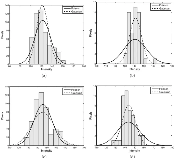
3.4 Intensity histograms with approximated distributions. . . 31
3.5 Concept of median filtering in image processing. . . 33
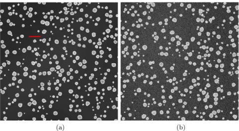
3.6 Gold on carbon sample images used for demonstrating ACF-based SNR estimation technique.. . . 35
3.7 ACF curve and the estimated noise free peak for a noisy gold on carbon
image. . . 35
3.8 Artificially generated images to analyze the filter response.. . . 36
3.9 Plots demonstrating the effect of blurring. . . 37
3.10 Filtered and the obtained noise images of silicon microparts sample. . . . 38
3.11 Artificial gold on carbon images generated by Artimagen to the precision of developed method.. . . 39
3.12 Gold on carbon images acquired with different scan times. . . 40
3.13 SNR evolution with respect to dwell time. . . 41
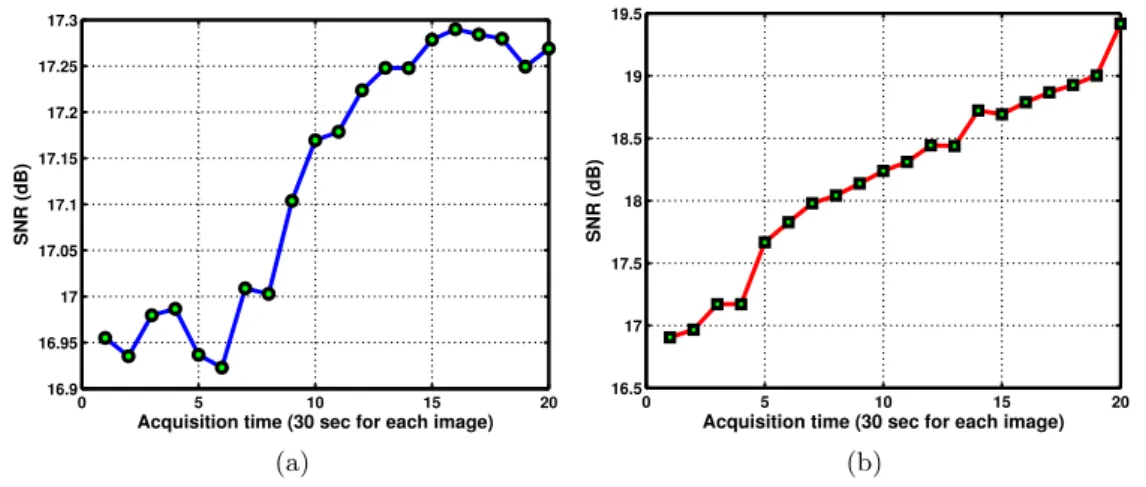
3.14 SNR vs. acquisition time at 40, 000× magnification. . . 42
3.15 SNR vs. acquisition time at 70, 000× magnification. . . 42
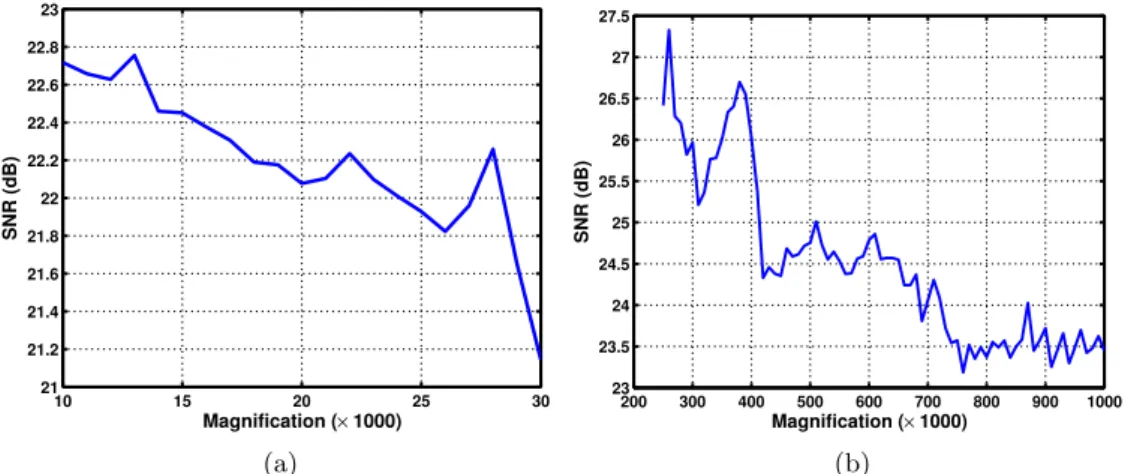
3.16 Evolution of SNR with respect to magnification. . . 43
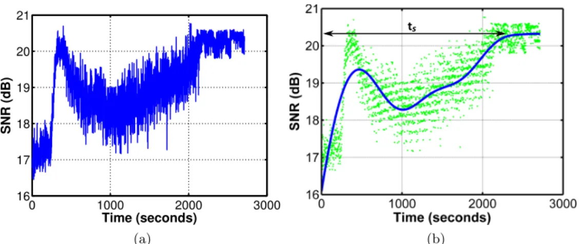
3.17 Plots showing real time SNR evaluation on day-1.. . . 44
3.18 Plots showing real time SNR evaluation on day-2.. . . 44
3.19 SNR variation with image focus. . . 45
3.20 Images of gold on carbon sample acquired at different times.. . . 47
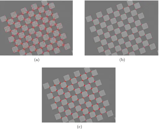
3.21 Keypoints computed for a microscale chessboard pattern. . . 50
3.22 Keypoints computed for gold on carbon sample.. . . 51
3.23 Keypoints matching using RANSAC. . . 52
3.24 Images depicting the real-time drift compensation at different magnification. 55 3.25 Disparity maps computed using reference and corrected images at differ-ent magnification.. . . 56
3.26 Evolution of the drift at different magnifications. . . 57
3.27 Evolution of drift with respect to time and magnification. . . 57
4.1 SEM probe movement model and operating principle. . . 63
4.2 Focusing geometry and different focusing scenarios in a SEM. . . 64
4.3 Relationship between the focus step and working distance. . . 65
4.4 The principle of autofocusing in SEM. . . 66
4.5 Performance of various sharpness functions. . . 69
4.6 Sharpness score variation with respect to focus steps. . . 71
4.7 Images depicting the level of details at various locations. . . 71
4.8 Secondary task variation with respect to the focus steps and sharpness score. . . 73
4.9 Microscale calibration rig with chessboard patterns used for imaging. . . . 75
4.10 Sharpness score and corresponding gain values at different magnifications. 75 4.11 Secondary task variation at different magnifications. . . 76
4.12 Images obtained during autofocusing process. . . 76
4.13 Sharpness score, corresponding gain and secondary task values with in-creased brightness. . . 78
4.14 Sharpness score, corresponding gain and secondary task values with in-creased scan speed. . . 78
4.15 Sharpness score, corresponding gain and secondary task values with sili-con microparts sample.. . . 79
vii
4.16 Images demonstrating the autofocusing at different experimental conditions. 80
4.17 The objects used for the depth estimation experiments. . . 82
4.18 Principle of focusing and sharpness score variation with the presence of gripper. . . 82
4.19 Sharpness function indicating the gripper and micropart locations. . . 83
4.20 Focused ROIs of different micro-objects present in the scene. . . 83
4.21 Results of autofocusing at different regions for depth estimation. . . 84
4.22 Relationship between the aperture diameter and depth of focus in SEM. . 85
4.23 Relationship between the magnification and depth of focus in SEM. . . . 86
4.24 Segmented regions of the micro-objects after applying watershed trans-formation. . . 86
4.25 Images acquired for reconstruction with varying working distance. . . 87
4.26 Initially estimated depth map for the regions containing gripper fingers. . 87
4.27 Reconstructed images formed after surface approximation. . . 89
4.28 Reconstructed images formed after overlaying the original texture. . . 90
4.29 Gold on carbon sample stub for JEOL SEM. . . 90
4.30 Reconstruction images of gold on carbon sample stub. . . 91
4.31 Reconstructed gold on carbon stub image formed after overlaying the original texture.. . . 91
5.1 Images of the microgripper demonstrating the distortion during object movement.. . . 95
5.2 Classical look and move visual servoing. . . 96
5.3 Block diagram depicting PBVS. . . 98
5.4 Block diagram depicting IBVS. . . 98
5.5 Block diagram depicting 2 1/2 D visual servoing. . . 99
5.6 Silicon microparts used for the experiments. . . 101
5.7 Hysteresis curves of the piezo-positioning platform. . . 102
5.8 Voltage-displacement control model of the piezo-positioning platform. . . 102
5.9 Visual representation of the cost function for intensity-based visual servoing.103 5.10 Block diagram depicting intensity-based visual servoing. . . 105
5.11 Series of images depicting the intensity-based visual servoing at normal scan speed. . . 106
5.12 Parameter variation during intensity-based visual servoing at optimal scan speed. . . 107
5.13 Series of images depicting the intensity-based visual servoing at high scan speed. . . 107
5.14 Parameter variation during intensity-based visual servoing at high scan speed. . . 108
5.15 Series of images depicting the intensity-based visual servoing at high mag-nification. . . 108
5.16 Parameter variation during intensity-based visual servoing at high mag-nification. . . 109
5.17 Series of images acquired during nanopositioning at unstable conditions
using intensity-based method. . . 110
5.18 Parameter variation during intensity-based visual servoing at unstable conditions.. . . 110
5.19 Images demonstrating the variation of Fourier spectral descriptors with translatioin and rotation. . . 112
5.20 Cost function for Fourier-based visual servoing. . . 114
5.21 Block diagram depicting Fourier-based visual servoing. . . 115
5.22 Series of images showing the positioning task using Fourier-based visual servoing at normal scan speed. . . 116
5.23 Parameter variation during Fourier-based visual servoing at optimal scan speed. . . 116
5.24 Series of images showing the positioning task using Fourier-based visual servoing at high scan speed. . . 117
5.25 Parameter variation during Fourier-based visual servoing at high scan speed.118 5.26 Series of images showing the positioning task using Fourier-based visual servoing at high magnification. . . 119
5.27 Parameter variation during Fourier-based visual servoing at high magni-fication. . . 119
5.28 Series of images during nanopositioning at unstable conditions using Fourier-based method. . . 120
5.29 Parameter variation during Fourier-based visual servoing at unstable con-ditions. . . 121
6.1 Software architecture. . . 124
6.2 Client-server communication model. . . 125
6.3 The scanning area selection using DISS5 scan controller. . . 126
6.4 Architecture diagram for APROS3 software. . . 127
6.5 The software main window containing device control widgets. . . 128
6.6 The live image viewing window of the software. . . 128
6.7 The interface window for performing real-time drift compensation. . . 129
6.8 The interface window for autofocusing. . . 129
7.1 Disparity map showing the corrected and uncorrected pixels. . . 134
7.2 Applications planned for future.. . . 135
List of Tables
2.1 Comparison of different microscopes used for nanomanipulation. . . 14
3.1 Computed MSE values for various filter sizes. . . 37
3.2 Total processing time for different filter sizes. . . 38
3.3 Known and computed SNR values using the developed method for artifi-cial gold on carbon image with different filter sizes. . . 39
3.4 Homography parameters computed at 10,000× magnification. . . 54
3.5 Homography parameters computed at 20,000× magnification. . . 55
3.6 MSE at 10,000× and 20,000× magnification. . . 56
3.7 Total time taken for drift compensation. . . 56
3.8 Computed homography parameters at 10, 000× magnification. . . 58
3.9 Computed homography parameters at 15, 000× magnification. . . 59
3.10 Computed homography parameters at 20, 000× magnification.. . . 59
4.1 Computed polynomial coefficients to find the working distance. . . 65
4.2 Processing time for various sharpness measures . . . 70
4.3 Time taken and accuracy at optimal conditions.. . . 77
4.4 Time taken and accuracy at changed brightness. . . 77
4.5 Time taken and accuracy with change in the dwell time. . . 78
4.6 Time taken and accuracy with silicon dioxide sample at optimal conditions. 79 4.7 Time taken (seconds) by the proposed method with various α values. . . 80
5.1 Computed polynomial coefficients for x-axis. . . 102
5.2 Computed polynomial coefficients for y-axis.. . . 102
5.3 Estimated positioning accuracy (µm) achieved by both methods. . . 121
List of Algorithms
1 Visul servoing-based autofocusing in SEM.. . . 74
2 Shape reconstruction from focus in SEM. . . 88
List of Abbreviations
2 1/2 D Two and a half dimension.
2D Two dimensional.
3D Three dimensional.
ACF Auto-correlation function.
AFM Atomic force microscope.
ARMA Autoregressive moving average.
BRIEF Binary robust independent elementary features.
BSE Back scattered electrons.
CAD Computer-aided design.
CCD Charge coupled device.
CMOS Complementary metal oxide semiconductor.
CNT Carbon nanotubes.
CPU Central processing unit.
DFT Discrete Fourier transform.
DISS Digital image scanning system.
DNA Deoxyribonucleic acid.
EBID Electron beam induced decomposition. FAST Features from accelerated segment test.
FEG Field emission gun.
FIB Focused ion beam.
GUI Graphical user interface.
IBVS Image-based visual servoing.
ICP Inductively coupled plasma.
InGaAs Gallium indium arsenide.
IP Internet protocol.
MLTDEAR Mixed Lagrange time delay estimation autoregressive.
MSE Mean squared error.
NEMS Nano electromechanical systems. NSOM Near-field scanning optical microscope.
ORB Orient FAST and rotated BRIEF.
PBVS Position-based visual servoing.
PC Personal computer.
RAM Random access memory.
RANSAC Random sample consensus.
ROI Region of interest.
SE Secondary electron.
SEM Scanning electron microscope.
SIFT Scale-invariant feature transform.
SNR Signal-to-noise ratio.
SPM Scanning probe microscope.
STM Scanning tunneling microscope.
SURF Speeded up robust features.
TCP Transmission control protocol.
TEM Transmission electron microscope.
USB Universal serial bus.
Chapter
1
Context and contributions
Nowadays, nanotechnology is becoming more prominent in the world of sciences. It is expected to play an important role in the coming years with a wide range of applications in the fields of manufacturing, information technology, electronics, and healthcare. Due to the latest advances in nanotechnology, nanorobotics and multi-physics nanocharac-terization have gained a significant research interest. They have shown a considerable progress in the recent years, as it became possible to develop novel nanoscale devices and systems with increasing efficiency. The consequence of this growth is an increase in the need for developing reliable and state of the art techniques for nanomanipulation and characterization. Various works that are performed in these areas show a great progress; however, most of them are still isolated operations. This work aims to capitalize on the recent surge in nanorobotics and robust control strategies for manipulation and try to apply them to this problem.
The work performed during this thesis is mostly concentrated or revolved around two themes: vision using SEM towards material characterization and automatic ma-nipulation, and visual servoing for precise nanopositioning. This work (using SEM vision) is a first of its kind that is performed in the department of AS2M (automation and micromechatronics systems). It has been performed in the context of ANR P2N NANOROBUST project that is briefly presented below.
1.1
Context
1.1.1 NANOROBUST project
The term NANOROBUST is the abbreviated form of the French national project entitled “multi-physics characterization and robotic manipulation of nano-objects under SEM”. It was started on November 28, 2011 with a duration of 48 months. The overall work is divided among the four partners of the project: FEMTO-ST (Besan¸con), ISIR (Paris), IRISA (Rennes) and LPN (Marcoussis). The main objective of this project is to perform fundamental research in the field of nanoscale characterization and manipulation.
The two typical applications that are studied as a part of this project are the in situ characterization of nanostructures for optical NEMS (nanoelectromechanical systems) such as quantum dots, nanowires and nanomembranes, and manipulation of nano-objects under SEM (scanning electron microscope) for observation with TEM (transmission electron microscope). Two types of characterization are considered. The first one aims to determine the physical properties (mechanical, thermal, electrical) of the nanostructures. The initial step in this process is the extraction and placement of these nanostructures on the characterization support. Then the robotic systems can move the sensors along a predefined path for property analysis of the positioned structure. These sensors can be either passive such as a simple AFM (atomic force microscope) tip whose deformation is measured from images or active such as a tuning fork that operates on the frequency drift to evaluate the stiffness of nano-objects.
The second type of characterization is aimed to determine the structural properties of the nanostructures for visual observation with TEM. Analysis of these objects requires precise positioning on a grid that is used inside TEM. A typical example is quantum dots where the nano-objects measure a few nanometers up to a few tens of nanometers in diameter. Standard preparation techniques become unsuitable for observing such nano-objects mostly because of the size and also very time consuming because of their low density. A solution could be by etching the micron sized walls on a semiconductor where the quantum dots will lie on top of these walls. The walls will then be displaced by a controlled nanomanipulation and placed on the TEM observation grid (see figure
1.1).
Figure 1.1: Illustration of the problem of handling a nano object on a TEM grid. (a) A series of walls of 2 µm obtained by ICP (inductively coupled plasma) etching on epitaxial substrate. (b) Observation TEM grid held by a gripper with two micromanipulators. (c) TEM grid with a ”wall” made (in the circle).
Both tasks are challenging mainly because of the size of nanostructures and requires the development of
• Accurate and reliable handling
• Precise and robust positioning schemes • Defectless or distortion free SEM imaging
1.1 Context 3
1.1.2 Project organization and structure The overall project can be described in the following steps
• Preparing the nano-objects (preparation)
• Handle, transport and placement of nano-objects (manipulation) • Performing characterization
Figure 1.2shows these three stages taking place in situ in the SEM.
MicrorobotTtrajectoryT controlTusingTvisualTservoing GripperTwithTforceTcontrol LocationTfor Tcharacterization AnalysisTofTcharacteristicsTby SEMTmeasurementsTorT forceTfeedback TestTsample -TVisualTservoingTofTtheTmicrorbotT TTTbyTSEMTimages -TTForceTcontrolTofTtheTgrippingT -TTCharacterizationTusingTSEMTTTTTTTT TTTTvision -TTCharacterizationTusingTintegrated TTTsensors Preparing nanoobjects Transport & Positioning Characterization
Figure 1.2: Studied process types of the NANOROBUST project.
The overall structure of the project is comprised of six tasks (see figure1.3) that are briefly presented below.
Task-1: Coordination
This task aims for efficient coordination of different stakeholders. All the partners are responsible for this task.
Task-2: Strategies for micro / nano-handling and characterization The main role of this task is to:
• Define gripping strategies that are adapted to the range of objects with different shape and size (e.g. handling / gripping objects like nanoballs or nanowires that may be embedded in a substrate).
• Define techniques for physical characterization of the objects. ISIR and FEMTO-ST are responsible for this task.
Tasku4:uSEMuImagingu anduvision Tasku2:uStrategiesuforu handlinguCucharacterization Tasku3:uRobustucontroluforu handlinguCucharacterization Tasku6:uIntegrationuCu validation Tasku5:uVisualuservoingu withuSEM Tasku1:uCoordination
Figure 1.3: NANOROBUST project tasks and coordination. Task-3: Robust control for precise handling and characterization The main objective of this task is to:
• Study and model the working conditions in a SEM, particularly noise and pertur-bations.
• Develop robust control laws for the control of micro / nanorobots.
• Increase the accuracy of micro / nanorobots by using refined control methods. FEMTO-ST and ISIR are responsible for this task.
Task-4: SEM imaging and vision This task aims to perform:
• Evaluation and compensation of noise and drift in real-time. • Modelling and calibration of distortion and projection. FEMTO-ST and IRISA are responsible for this task.
Task-5: Visual servoing with SEM
This task aims to achieve the manipulation of objects by visual servoing approaches. It includes:
1.2 Thesis outline - author’s contributions 5
• Computing the interaction matrices. • Calculation of the control laws.
IRISA and FEMTO-ST are responsible for this task. Task-6: Integration and validation
This is the final task to integrate all the other tasks and to validate the performance of manipulation techniques in SEM for characterization of nanoscale objects. LPN is responsible for this task.
1.2
Thesis outline - author’s contributions
The work performed during this thesis is included in the tasks 4 (chapter 3) and 5 (chapters 4 and 5) of the project. The remainder of this document showing the author’s contributions towards vision and visual servoing for nanomanipulation and nanocharac-terization is organized as follows:
Chapter 2 presents the existing state of the art in the field of nanorobotics and nanomanipulation. It provides a comprehensive study and a comparison of various microscopic systems available for imaging at nanoscale. Different nanomanipulation systems that are used in other works are analyzed along with their corresponding appli-cations. Apart from this, an overall description of SEM imaging system along with the used hardware set-up is detailed at the end.
Chapter 3 provides solution for two major problems with SEM imaging: noise and drift. It is a well-known fact that SEM imaging is mostly affected by the non-linearities and instabilities present in the electron column along with the addition of huge amount of noise with high scan rates. This chapter starts with a detailed description towards the noise in SEM imaging. Different techniques and methods that are available for quantifying the level of noise are studied. A simple and real-time method that has been developed for quantifying the noise level and monitoring the image quality is presented. For the problem of drift, an image registration-based method is presented for correcting the drift in real-time. It has been compared with the well-known correlation-based method. Drift compensation is performed at high magnifications (10k × − 30k×) using a gold on carbon sample.
Chapter 4 presents the work performed using SEM image focus i.e. autofocus, depth estimation from focus for nanomanipulation and shape reconstruction from focus. It mainly highlights the importance of focus with SEM imaging. While performing an automated vision-based manipulation task, it is important to provide sharp images in order to gain full advantage of the visual measurements as well as to accomplish the task with a good precision. To solve this, a visual servoing-based method to perform efficient autofocusing has been developed. The developed method is robust and fast in
comparison to the traditional search-based techniques. Besides, acquiring inter-object depth information to use it for nanomanipulation is a crucial and difficult task with SEM, since it possess a single imaging sensor. This problem is solved by performing region-based autofocusing. Apart from these, a focus-based method to reconstruct the 3D shape of the objects being viewed is presented. It helps in gaining the knowledge of imaging scene.
Chapter 5 presents the vision-based automatic nanopositioning under SEM. It starts with an overview of the key topics in nanopositioning and state of the art in visual servoing. The nanopositioning studied in this chapter is to perform characterization of microstructures by probing to measure the structure stiffness and to perform in situ manipulation of micro-nanostructures. Because of the presence of high amount of imag-ing noise and distortions, it is difficult to rely on any feature trackimag-ing-based methods. Considering this problem, two visual servoing-based approaches are presented that do not require any tracking and instead, they use the complete image information. The first one is the intensity-based method that has been implemented using the idea of photometric visual servoing approach. This method uses the overall pixel intensities as visual measurements. The second one is a Fourier domain method. With this method, the 2D motion between the images is considered as visual measurement. For a task of positioning silicon micro-objects using both methods, the control strategies are designed to minimize the positioning error by controlling the platform movement.
Chapter 6 is dedicated to the software development during the thesis. In fact, this thesis is started from the scratch and it is our primary objective to set-up and program different modules for synchronous operation. Out of all, the most important and primary task performed is the development of software libraries for continuous image acquisition and SEM parameter control. A software user interface application has been developed in order to reduce the operational complexity and process monitoring.
1.3
List of author’s Publications
International conferences and workshops Accepted and published
1. Naresh Marturi, Brahim Tamadazte, Sounkalo Demb´el´e, and Nadine Piat, “Vi-sual Servoing Schemes for Automatic Nanopositioning in Scanning Electron Micro-scope”, In IEEE International Conference on Robotics and Automation (ICRA’14),in-press.
2. Naresh Marturi, Sounkalo Demb´el´e, and Nadine Piat, “Depth and Shape Esti-mation from Focus in Scanning Electron Microscope for Micromanipulation”, In IEEE International Conference on Control, Automation, Robotics and Embedded systems (CARE’13), in-press.
1.3 List of author’s Publications 7
3. Naresh Marturi, Brahim Tamadazte, Sounkalo Demb´el´e, and Nadine Piat, “Vi-sual Servoing-Based Approach for Efficient Autofocusing in Scanning Electron Mi-croscope”, In proceedings of the IEEE/RSJ International Conference on Intelligent Robots and Systems (IROS’13), pp. 2677-2682, 2013.
4. Naresh Marturi, Sounkalo Demb´el´e, and Nadine Piat, “Fast Image Drift Com-pensation in Scanning Electron Microscope Using Image Registration”, In proceed-ings of the IEEE International Conference on Automation Science and Engineering (CASE), pp. 807-812, 2013.
5. Naresh Marturi, Sounkalo Demb´el´e, and Nadine Piat, “Performance evalua-tion of scanning electron microscopes using signal-to-noise ratio”, In Internaevalua-tional Workshop on MicroFactories (IWMF’12), Finland, pp. 1-6, 2012.
6. Sounkalo Demb´el´e, Nadine Piat, Naresh Marturi, Brahim Tamadazte, “Gluing free assembly of an advanced 3D structure using visual servoing”, In Micromechan-ics and Microsystems Europe Workshop, Germany, 2012.
International journals Accepted
7. Abed Malti, Sounkalo Demb´el´e, Nadine Piat, Claire Arnoult, Naresh Marturi, “Toward Fast Calibration of Global Drift in Scanning Electron Microscopes with Respect to Time and Magnification”, In International Journal of Optomechatron-ics, Taylor and Francis, vol. 6, no. 1, pp. 1-16, 2012.
8. Naresh Marturi, Sounkalo Demb´el´e, and Nadine Piat, “Monitoring the Sig-nal to Noise Ratio of a Tungsten Gun Scanning Electron Microscope for Micro-Nanomanipulation”, In Scanning, in-press.
In preparation
9. Naresh Marturi, Sounkalo Demb´el´e, and Nadine Piat, “Efficient Depth esti-mation Technique in Scanning Electron Microscope for Nanomanipulation”, In preparation.
10. Naresh Marturi, Sounkalo Demb´el´e, and Nadine Piat, “Accurate Nanoposition-ing in ScannNanoposition-ing Electron Microscope for nanocharacterization”, In preparation.
Chapter
2
Introduction to nanomanipulation and
SEM imaging
In this chapter, various background details regarding the nanoscale manipula-tion are presented. Starting from the basic topics related to the nanorobotics and nanomanipulation, we approach and highlight the role of the imaging sensors in assisting the manipulation of objects at nanoscale. Apart from this, a complete description of a SEM system along with the system hard-ware set-up used for this thesis are presented.
2.1
Background
With a rapid development in micro-nanoscale technology in the last couple of decades, handling nanometric objects for building complex NEMS-based products has gained a significant research interest. Since the human handling is not a feasible option (almost impossible) at this particular scale, nanorobotics has been emerged as a new field to tackle this critical issue. In general, Nanorobotics deals with the study, design and application of robotic devices close to nanoscale. Specifically, it is concerned with ma-nipulation and assembly of nano-objects using micro or macro devices and programming of robots with overall dimensions at nanoscale [Req03]. It integrates together various disciplines including nanofabrication processes that are used to produce nanoactuators, nanosensors etc., nanorobotic assembly, self-assembly, nanomaterial synthesis, nanochar-acterization and nanobiotechnology [DN07].
Being a new field, nanorobotics has been mainly classified into two research ar-eas [Req03,Sit07]. The primary area concerns developing new methods for nanomanip-ulation and assembly of micro-nanometric objects of interest. Here, the main idea is to design and control large micro-nanorobotic systems that are able to handle nanomet-ric objects with good precision [FE08,BF12]. These approaches are called as top-down methods that use well-known processes from semiconductor industry to fabricate small structures with optical lithography. On the other hand, the second area i.e. the bottom-up approach is dedicated to manufacture new mobile robotic systems with various capa-bilities whose overall size is in the range of few micrometers. The bottom-up strategies are generally assembly-based techniques and include techniques such as self-assembly, directed self-assembly etc. For developing these systems, the overall size is a major constraint that makes it challenging to integrate different devices like actuators, sen-sors etc. altogether. Even though the size miniaturization has been progressed recently using microfabrication techniques, there exist a lot of difficulties in achieving further miniaturizations. Due to this problem, not much work related to nanomanipulation has been performed in this area. In the meanwhile, the former approach has turned out to be one of the possible solutions for handling nano-objects.
In general, nanorobotic manipulation can be defined as the manipulation of nanoscale objects where, contact and surface forces dominate the volume related properties affect-ing: handling (pick, place, release etc.) and positioning (accuracy, rotation, orientation etc.) operations. So far, considerable research has been performed towards the devel-opment of these systems [Sit01]. A basic nanomanipulation system consists of nanoma-nipulators (figure2.1(a)) and platform stages for positioning, microscopes for task space perception, handling devices such as microgrippers (see figure2.1(b)), microprobes for object grasping and different sensors that are integrated with gripper fingers to assist the manipulation process. Apart from these, it also contains a programmed interface for synchronous operation of all the system components. Basically, all these components are mounted on a vibration isolation system to reduce the effect of external environ-mental disturbances. Most of the time, the manipulation tasks are performed in high vacuum conditions to prevent the sample contamination. The schematic diagram of a basic nanomanipulation system is shown in the figure2.2.
2.1 Background 11
(a) (b)
Figure 2.1: (a) Kleindiek MM3A robotic micromanipulator [Gmb] (b) FEMTO TOOLS FTG 32 microgripper [Fem11].
Controller Human-machine
interface
Manipulator View sensor
Actuator Positioning stage
Force sensor
Nano-objects
Figure 2.2: Schematic diagram of a basic nanomanipulation system. 2.1.1 Nanoscale imaging
In 1878, Ernst Abbe proved that the resolution of the optical microscope is limited by the wavelength of light and the smallest detail that can be resolved is of the order of few micrometers [Fre63]. With the two famous discoveries: the moving electron wave properties by de Broglie in 1924 and the effect of magnetic coil on an electron beam by Busch in 1926-27, many researchers started to work on imaging extremely small objects with electron beam. In 1931, Max Knoll and Ernst Ruska from Technical University of Berlin, Germany successfully built and demonstrated the first electron microscope (figure 2.3).
Apart from electron microscopy that includes TEM and SEM, nanoscale imaging can also be carried out using SPM (scanning probe microscope) technique that includes AFM, STM (scanning tunneling microscope) and NSOM (near-field scanning optical microscope). Except SEM that has been explained in the next section, the rest of the imaging techniques are briefly explained below. A comparison of all these devices is provided in the table2.1.
Figure 2.3: The first electron microscope demonstrated by Max Knoll and Ernst Ruska in 1931 [Fre63].
Transmission electron microscope
Belonging to the family of electron microscopes, a TEM (figure 2.4) uses high energy electrons for imaging. It was built by James Hillier and Albert Prebus at the University of Toronto in 1938. It operates at high voltages ranging from 50−1000 kV and provides a resolution up to 0.1 nm. With TEM, a beam of electrons are produced and transmitted through an ultra-thin sample. Later, the unscattered electrons that are transmitted through the sample hit a fluorescent screen at the bottom of the microscope producing the image. By adjusting the voltage of the gun, the speed of the electrons can be modified which inturn modifies the image. Generally, the images produced by TEM are gray scale and can be interpreted as follows: the lighter areas represent the higher number of electrons transmitted and the darker areas represent lower number and dense areas on the sample. To use with TEM, samples need to be sliced thin enough for electrons to transmit.
Scanning tunneling microscope
STM (figure 2.5) is the first type of SPM that was invented by Binnig and Rohrer in 1982. The STM is comprised of a piezoelectric linear stage and an extremely fine conducting probe that is held close to the sample surface. The probe tip is extremely sharp formed by a single atom. This atomic sized tip is moved across the sample surface in a raster pattern during which the electrons tunnel between the surface and probe generating an electric signal. In order to maintain a constant signal, the probe is raised and lowered during the scanning process. The current used to keep the signal constant
2.1 Background 13 Electron source Condenser lens Condenser aperture Objective lens Objective aperture Selected area aperture Projective lens Intermediate lens Screen Sample
Figure 2.4: Transmission electron microscope schematic diagram.
is used in generating the images. Similar to TEM, a STM is also capable of providing atomic resolution. However, STM can be used only with conducting sample surfaces and provides only surface topographical information.
Sample stage nA tunneling electrons sample surface Probe Piezo Stage sample
Atomic force microscope
The AFM (figure2.6) was invented by Binnig, Quate, and Gerber in 1986 to overcome the conductivity requirement associated with STM. Similar to STM, an AFM uses a cantilever (made of silicon or silicon nitride) with a sharp tip (radius of few nanometers) to scan the sample surface. When the tip is placed near the sample surface, the forces between the surface and tip deform the cantilever according to Hooke’s law [BQG86]. In a typical system, this deflection is monitored by reflecting a laser from the top of the cantilever on to an array of photodiodes. Based on the type of application, different imaging modes (contact, non-contact, lateral force, phase imaging etc.) can be used with AFM. The main advantage of AFM is that it can image any kind of surfaces. The lateral resolution provided by an AFM is 1 nm.
Laser source Photodiode Microcantilever Tip Sample Piezo element Force Surface atoms Tip atoms
Figure 2.6: Atomic force microscope schematic diagram.
Table 2.1: Comparison of different microscopes used for nanomanipulation.
Property STM AFM TEM SEM
Imaging principle tunneling inter-atomic electrons electrons electrons forces
Environment air / vacuum all vacuum vacuum
Dimension 3D 3D 2D 2D
Samples conductors All conductors conductors
semi-conductors semi-conductors semi-conductors Resolution > 0.01 nm > 0.1 nm > 0.01 nm > 1 nm Interaction non-contact non-contact / non-contact non-contact
contact
2.1.2 Nanomanipulation systems
The existing nanomanipulation systems can be broadly classified into different types based on the starting point, manipulator-object interaction, utilized nanomanipula-tor interaction and the technique used for overall system operation as shown in fig-ure 2.7 [Sit01]. The first works on nanomanipulation are known to be performed in 1990 by Eigler and Schweizer [ES90], who managed to position individual Xenon atoms
2.1 Background 15 Nanomanipulation approaches Starting point-based Process-based Interaction type-based Operation-based Top-down Bottom-up Self-assembly Physical Contact Contactless Tele-operated Semi-autonomous Automatic
Figure 2.7: Classification of nanomanipulation systems provided by Sitti [Sit01]. in the shape of IBM logo on a single-crystal nickel surface at low temperatures using STM(figure 2.8). Since then, many research groups started working on nanomanipula-tion using AFM [SRPA95,HKS+98,VSZ04]. The main advantage of using the AFM as a micro-nanomanipulator is its use of single sensor to sense force and 3D topography. Many research groups have showed 2D precise positioning of nanoparticles or CNTs (carbon nanotubes) on surfaces using contact pushing following a look and move control scheme. However, the main difficulty comes in imaging and manipulating the object si-multaneously in real time. To solve this, many works have used AFM probes with SEM as it is capable of scanning at near real-time [EG94,FSF02,MWJF10]. Apart from using AFM tips, many systems have used piezoelectric actuators for accurate nanopositioning during nanomanipulation as they are capable of providing smaller displacements. These devices are operated by varying voltage across the piezoelectric element. However, these actuators suffer from a major problem of non-linear hysteresis.
For the first time, micro-nanomanipulation using a SEM has been reported and per-formed by Hatamura and Morishita [HM90] and Sato et al. [SKMH95]. Their manipula-tion system consists of two micromanipulators to manipulate micro-objects smaller than 100 µm. In their work, to achieve high positioning accuracy, piezoelectric actuators and parallel plate structures are used. Yu et al. have presented a nanomanipulation system to perform 3D manipulation and characterization of CNTs [YDS+99]. The manipulation is performed in open-loop under slow-scan mode. Fukuda et al. has presented a 16 degrees of freedom nanomanipulation system positioned inside a SEM chamber for the assembly of nanodevices with multiwalled carbon nanotubes [FAD03]. Using this system, they have performed the connections between nanotubes using EBID (electron beam induced decomposition) and mechanochemical bonding. Thereafter, many research groups have reported manipulation of CNTs under SEM [NA03,MHMB04]. In their work, Molhave et al. have used microfabricated, electrostatically actuated tweezers for handling the
Figure 2.8: A sequence of images taken during the manipulation and arrangement of Xenon atoms [ES90].
nano-objects [MHMB04]. Fatikow et al. have presented an automated nanohandling station inside the SEM chamber [FWH+07]. It consists of two multi degrees of freedom mobile microrobots for positioning the specimen and the end-effector, a CCD (charge coupled device) camera for monitoring platform movement and a touchdown sensor for contact detection and depth estimation. With this setup, they have demonstrated an automated task of handling TEM-lamellae using vision feedback. Considering the prob-lem of using SEM images as feedback information i.e. too noisy with high scan speeds and slow acquisition rate, recently Jasper has presented a new line scan-based posi-tion tracking system that is integrated with SEM [Jas09,Jas11]. The new system can determine the position of the objects using few line scans instead of acquiring global image.
2.1.3 Applications of nanomanipulation
So far in the literature, nanomanipulation systems are widely used in many fields for various applications. Some of them are listed below.
Biotechnology:
The development of new nanomanipulation techniques has given researchers the ability to manipulate single biomolecules and to record mechanical events of biomolecules at the single molecule level [IIY01]. It is also used for controlled manipulation of biological cells,
2.2 SEM Imaging 17
molecules and tissues, DNA (deoxyribonucleic acid), proteins, adenovirus etc. [GMN+99, GFM+00]. Besides, it is also used for measuring the twisting and bending compliance of DNA [Was03].
Material science:
Nanomanipulation plays an important role in building new materials and for analyzing the material properties such as friction, adhesion, electrical, optical etc. As mentioned earlier, many research groups have been working on manipulating and assembling of CNTs. The recent research investigations on CNTs report many suitable properties to use them in nanoscale electronics, mechanics etc. Apart from property analysis, nanomanipulation is also used in preparing samples such as TEM lamella (figure 2.9), nanowires etc.
Figure 2.9: TEM sample lift-out using an extraction needle [Nan12].
Apart from the above mentioned applications, nanomanipulation has also its appli-cations in computer technology for data storage [BDD+99,JJJ+09].
2.2
SEM Imaging
The SEM is a most widely used instrument of all the available electron microscopes. One of the most important aspects of SEM is its ability in producing the images of three-dimensional specimens at high magnifications and high resolution (better than 1 nm). Unlike optical microscopes, a SEM produces images of a sample by raster scanning the sample surface with a focused beam of high energy electrons. In this section, various details regarding the SEM instrumentation and its operating principle are explained. 2.2.1 SEM components
The basic architecture along with the major components present inside a SEM electron column is shown in the figure 2.10. All these components perform different roles in generating the electron micrographs. The main components are described below and more details can be found in [GNJ+03].
Aperture Selector Vacuum Chamber Sample stage Objective Lens Scan coils Condenser lens Anode Electron gun Tilt + height adjustment Platform
Figure 2.10: Conventional SEM architecture illustrating various components. Vacuum system
A vacuum system is one of the mandatory requirements when working with elec-tron beam. It is mainly responsible to avoid collisions between elecelec-trons and the extraneous gas molecules and protecting the filament from oxidation. Without ad-equate vacuum inside the SEM column, an electron beam can neither be created nor controlled. Typically, most of the available SEMs operate at vacuum of 10−4 to 10−6 Torr. In order to achieve this pressure, two types of pumps are used: low vacuum pump or roughing pump and oil diffusion pump. Roughing pump is a type of mechanical pump that provides pressure down to 10−3 Torr and thereafter high vacuum is achieved by oil diffusion pump.
The electron gun
An electron gun (see figure 2.11) is comprised of an electron emitter, a Wehnelt cylinder and an anode. Available electron guns with present day SEMs are con-ventional electron guns using Tungsten (W) hair-pin, or lanthanum hexaboride (LaB6) tips and field emission guns (FEG) . With the conventional guns, a sta-ble number of electrons are emitted by supplying the necessary filament heating current. On the other hand, FEG (cold emission source) uses the difference in the potential between cathode and anode to excite the electrons. The Wehnelt
cylin-2.2 SEM Imaging 19
der that encloses the filament acts as a cathode. It contains a small hole in the center through which the generated electrons are centered and exited. Finally, a positively charged anode that is rested under the Wehnelt cap is used to accelerate the electrons. The portion of the electrons that passes through the anode is called as beam current. In general, the acceleration voltage that is supplied to anode varies from less than 1kV to 30kV . A high value for acceleration voltage reduces the beam diameter and increases the resolution. But a too high value leads in charging up and damaging the specimen.
Wehnelt cylinder
Filament
Anode
Figure 2.11: Schematic diagram of a SEM electron gun showing various components. Electromagnetic lenses
The two sets of electromagnetic lenses that are available in an electron column are the condenser lenses and the objective lenses. Condenser lenses lying above the aperture strip are mainly responsible for controlling the electron concentration and the diameter of the beam. Objectives lenses that are present under the aperture converges the incoming beam and focus it on the sample surface.
Objective aperture
It is a metal rod holding a thin metallic strip (aperture strip) containing small holes (apertures) of different diameters. It is mainly responsible to filter the low energy and non-directional electrons. The aperture size is selected based on the type of the work. For low magnifications a larger aperture can be used and for high resolution imaging a small aperture is required. However, a smaller aperture leads in dark images as the count of the electrons interacting with sample surface is less.
Scan coils
The two sets of scan coils that are available in the electron column are used to raster the electron beam in both horizontal and vertical directions on the sample surface. The first pair deflects the beam off the optical axis and the second pair bends the beam back on to the axis at the pivot point of the scan (see figure2.12). Apart from scan generation, they are also used in controlling the magnification of the instrument.
1st scan coils 2nd scan coils Objective lens pole piece Sample e- beam
Figure 2.12: Beam deflection by scan coils inside the SEM. Electron detectors
In general, a SEM consists of various detectors each of which is used to collect different types of emitted electrons. The commonly used detectors are SE detec-tor and BSE detecdetec-tor. Two types of SE detecdetec-tors are available with the modern SEMs. The primary type is the most commonly used Everhart-Thornley detector that is fixed to the side walls of the chamber (see figure 2.13). It works by at-tracting the emitted secondary electrons by a positive potential applied to a ring around the detector. The second type is in-lens detector that is fixed alongside the electromagnetic lens. BSE detectors are located just below the pole piece of the object lens and collects the emitted back scattered electrons.
Figure 2.13: SEM chamber showing the secondary electron detector and mobile platform to place samples.
Positioning platform
2.2 SEM Imaging 21
column and is used to load the specimen. It can be controlled using a joystick and contains translational (X, Y , Z), rotational (around Z) and tilt (horizontal) movements. It is mainly responsible for better positioning the sample such that it is well exposed to the electron beam.
2.2.2 Operation principle
Before dealing with the actual image acquisition process, it is important to know the electron beam interaction with the specimen surface and the emission of various signals that are resulted during this process.
Beam - sample interaction
When a focused beam of electrons hits the sample surface, they penetrates into it for some distance (about 1µm) before hitting another particle. These incident electrons are greatly scattered resulting in elastic and inelastic scattering inside the sample forming a region called as interaction volume1. Elastic scattering results in BSEs (back scattered
electrons) where as inelastic scattering produces SEs (secondary electrons), Auger elec-trons and X-rays. Figure 2.14 shows the interaction of electron beam with a specimen surface and signal emission. The resulted electrons are recorded at their respective de-tectors. Out of all the emitted signals, SE and BSEs are the most widely used ones and are explained below. More information about SEM interaction volume can be found in [GNJ+03,Rei98]. Electron beam Auger e-Sample surface Secondary e-Characteristic X-rays Back scattered e- Bremssrahlung X-rays Electron interaction volume
Figure 2.14: Interaction volume and signal emission.
1The resulting region over which the incident electrons interact with the sample to produce different
signals is termed as interaction volume. Its volume depends on the beam acceleration voltage, specimen topography and the angle of incidence of the primary beam.
Back scattered electrons: These are the original beam of electrons that are escaped after the beam-sample interaction. These electrons have approximately the same energy as that of the primary ones and are easy to record. The images formed using the BSEs provide compositional differences, specimen topography, crystal orientation and grain boundaries. Figure2.15(b) shows the BSE image of a fractured aluminium alloy. Secondary electrons: These electrons are produced when an incident electron ex-cites a weekly bonded outer shell electron (in conductors) or a valence electron (in semi-conductors and insulators). During this process the electrons from the specimen receive kinetic energy from the incident electrons and start moving towards the surface. Mostly, the SEs are emitted by the atoms near the specimen surface. Moreover, the num-ber of SEs is greater than the incident electrons due to the multiple scattering events which subsequently increase the signal level. So with SE mode, the spatial resolution in an image is high. The images formed using the SEs provide surface topography and morphology. Figure2.15(a) shows the SE image of a fractured aluminium alloy.
(a) (b)
Figure 2.15: (a) SE image and (b) BSE image of a fractured alluminium alloy [Mik04].
Image acquisition
The image acquisition process starts with the beam generation. Initially, an accelerat-ing voltage is supplied to the electron gun to produce the electrons. These electrons that are redirected by the anode traverse the electron column vertically. The series of electromagnetic lenses and apertures present in the electron column control the beam diameter and focus it on to the sample surface. Finally, to acquire an image, a region on the sample surface has to be scanned by the electron beam in both horizontal and vertical directions with a great speed. This is then performed by the scan coils (one for each direction) by varying the current passing through them as a function of time. As a result of the beam interaction with sample surface, different signals are emitted. The resulted electrons are recorded at their respective detectors and then the gathered in-formation is amplified, digitized and recorded as an image. As the electrons wavelength is much smaller than visible light, no color image can be produced using a SEM. Here
2.3 Experimental hardware set-up 23
an interesting fact about SEM is, unlike optical systems no lens is directly involved in image acquisition. Figure 2.16shows the image formation process in SEM.
electron beam
Area scanned on sample Pixels displayed on the monitor
Secondary electrons
Detector
Image acquisition system
Figure 2.16: Image formation process in a SEM.
In SEM, each pixel is captured individually in a quick succession. The intensity value of a pixel depends mainly on the interaction position of the beam on the sample surface. For a scan length N on the sample surface, the generation of one raster line R is given by equation (2.1). Rn= N X i=1 I(xn, yi) (2.1)
where, n = 1 to M lines, x and y are the row and column indices of the interaction point. The total time taken (tn) to produce one raster line is given by equation (2.2).
tn= N tpn + (n − 1)tld (2.2)
where, tp is the time to produce one pixel given by tD + td, tD is the dwell time2, td is the time delay between the pixels and tld is the line delay between two raster lines. At n = M , tn becomes the time to produce one single scan image. Besides, the size of a pixel depends on the size of the beam (spot size or probe size) hitting the sample surface. It can be controlled by changing the current passing through the condenser lens. Spot size mostly affects the image resolution. Higher is the spot size, lower is the image resolution. Typically, higher spot sizes are used for low magnification imaging. The magnification in a SEM can be changed by changing the excitation voltage through the scan coils and it is defined as the ratio of the length of the scan on the monitor to the length of the scan on the sample surface.
Figure 2.17: Experimental environment showing the hardware set-up.
2.3
Experimental hardware set-up
The hardware set-up architecture used for this thesis is shown in the figure 2.17. It consists of a JEOL JSM 820 SEM, an image acquisition system along with a SEM control computer and a work computer. The JEOL JSM 820 is a state-of-the-art tungsten source SEM. Its electron column is equipped with all the elements explained in previous section and its objective aperture strip contains 4 apertures of diameters 100 µm, 70 µm, 50 µm and 30 µm respectively. The accelerating voltage for the SEM varies from 0.3 kV to 30 kV and the achievable resolution at 30 kV is 4.5 nm. The magnification of the SEM varies from 10× to 100, 000× and the maximum allowable electronic working distance is 50 mm. The SEM chamber is equipped with a mobile platform that can be controlled externally using joystick. For this work, a new piezo positioning platform, TRITOR 100 (from piezosystemjena [Pie13]) having 3 degrees of freedom (X, Y and Z) has been mounted on the already available platform (see figure 2.13). It is vacuum compatible and is capable of producing motion up to 100 µm on all the three available axes with a resolution of 0.2 nm in open loop. Different axes of this piezo positioning stage are controlled by the NV 40/3 piezo voltage amplifier (from piezosystemjena [Pie13]). It also provides the facility to control the stage axes from remote work computer via serial port interface. Apart from these, a 3 degrees of freedom robot manipulator (Kleindeik MM3A) system is planned to fix inside the SEM vacuum chamber. The end effector
2
2.4 Conclusion 25
of the manipulator will be equipped with a FT G-32 force sensing microgripper (from Femto tools [Fem11]). The maximum opening between the fingers of the gripper is 30 µm and their movement can be controlled by varying the actuation voltage. The incoming readings from the force sensors are recorded using a National Instruments data acquisition device (NI 6008 USB). Both the manipulator controller and gripper controllers are interfaced with the work computer.
The SEM control computer is solely responsible for controlling the microscope. It is connected to the image scanning system (DISS5) via USB and SEM electronics. The im-age scanning system provides an interface that runs from the SEM computer. It enables different functionalities for beam control (acceleration voltage, spot size, focus, magni-fication etc.) and manual image acquisition with a chosen dwell time. The maximum possible resolution of an image is 16, 384 × 16, 384 pixels and the maximum achievable acquisition speed is 3.1 frames per second using a dwell time of 360 ns. A software application to perform automatic image acquisition and control has been designed and is explained in the chapter6. On the other side, work computer is purely dedicated for performing the control operations using the images acquired from SEM computer.
2.4
Conclusion
Now, we have gained sufficient knowledge related to the concepts of nanorobotics, nanomanipulation systems and imaging at nano scale. Since manual control is a dif-ficult and tiresome task at this particular scale, using vision information seems to be a feasible solution. Up on comparing all the available imaging systems, SEM is proved to be more appropriate tool for performing real time manipulation tasks due to its high working range and the capability of providing near real time image feedback with high depth of field, high magnification and high resolution. However, it possess some major limitations and the most important one is the image quality that depends on the scale and speed of imaging and type of the material used. Added to this, time varying dis-tortion (explained in the next chapter) that is usually observed at high magnifications is another critical problem. So, in order to overcome some of these problems associated with SEM to use it for nanomanipulation, we propose some methods and solutions that are detailed in the next chapters.
Chapter
3
Image analysis and time-varying
distortion calibration in SEM
As a vision sensor, SEM performs a vital role in autonomous micro-nanomanipulation applications. Unlike optical microscopes, a SEM produces images of a sample by raster scanning the sample surface with a focused beam of electrons. When it comes to the sub micrometer range and at high scanning speeds, the images produced by the SEM are noisy and need to be corrected or evaluated before using them. Moreover, SEM im-age acquisition is mostly affected by the time varying motion of pixel positions in the consecutive images, a phenomenon called drift. In order to perform accurate measure-ments, it is necessary to compensate this distortion (drift) in advance. In this chapter, we present the methods to evaluate the SEM imaging quality along with the time varying distortion compensation. Various experiments have been performed at different operating conditions and the results are presented.
![Figure 2.3: The first electron microscope demonstrated by Max Knoll and Ernst Ruska in 1931 [Fre63].](https://thumb-eu.123doks.com/thumbv2/123doknet/14536978.724219/35.892.203.739.189.521/figure-electron-microscope-demonstrated-max-knoll-ernst-ruska.webp)
![Figure 2.8: A sequence of images taken during the manipulation and arrangement of Xenon atoms [ES90].](https://thumb-eu.123doks.com/thumbv2/123doknet/14536978.724219/39.892.203.739.188.557/figure-sequence-images-taken-manipulation-arrangement-xenon-atoms.webp)