HAL Id: hal-01763535
https://hal.archives-ouvertes.fr/hal-01763535
Submitted on 11 Dec 2020
HAL is a multi-disciplinary open access
archive for the deposit and dissemination of
sci-entific research documents, whether they are
pub-lished or not. The documents may come from
teaching and research institutions in France or
abroad, or from public or private research centers.
L’archive ouverte pluridisciplinaire HAL, est
destinée au dépôt et à la diffusion de documents
scientifiques de niveau recherche, publiés ou non,
émanant des établissements d’enseignement et de
recherche français ou étrangers, des laboratoires
publics ou privés.
Dielectric engineering of nanostructured layers
preventing electrostatic charging in thin dielectrics
K Makasheva, Christina Villeneuve-Faure, Caroline Bonafos, Christian
Laurent, Alessandro Pugliara, Bernard Despax, Laurent Boudou, G. Teyssedre
To cite this version:
K Makasheva, Christina Villeneuve-Faure, Caroline Bonafos, Christian Laurent, Alessandro Pugliara,
et al.. Dielectric engineering of nanostructured layers preventing electrostatic charging in thin
di-electrics. Nanotechnology Materials and Devices Conference (NMDC), 2015 IEEE, Sep 2015,
Anchor-age, United States. �10.1109/NMDC.2015.7439236�. �hal-01763535�
1
1Abstract—New dielectric-engineering concept is developed
intending a net improvement of the performance of dielectric layers under electrical stress. Instead of synthesis of new dielectric materials a new class of dielectric layers that gain their performance from design rather than from composition is established. Two kinds of nanostructured dielectric layers are
presented here: (i) silicon oxynitride layers (SiOxNy:H) with
gradual variation of their properties (discrete or continuous),
and (ii) SiO2 layers with tailored interfaces; a single layer of
silver nanoparticles (AgNPs) is embedded in the vicinity of the dielectric free surface. Modulation of the conductive properties of the nanostructured layers over 7 orders of magnitude is achieved. The nanostructured layers exhibit much shorter charge retention times and appear promising candidates for general applications where surface charging of dielectrics must be avoided, in particular for implementation in RF MEMS capacitive switches with electrostatic actuation.
Topic — MEMS/NEMS
Index Terms/Keywords — silver nanoparticles, silicon
nanoparticles, nanostructured dielectric layers, plasma processes
I. INTRODUCTION
THE electrostatic charging of thin dielectric layers represents an intensive field of scientific research, yet requiring a comprehensive study. The charge injection in dielectrics is at the origin of space charge formation [1, 2] leading in some cases to unexpected behaviour of the dielectric layers under electrical stress. Although the electrostatic charging of thin dielectric layers lays down the principle of operation of various technological devices, like non-volatile memories [3, 4], it is considered as the main cause of electrostatic sticking in MicroElectroMechanical Systems (MEMS) [5-7]. Indeed, the dielectric charging in RF MEMS switches is at the origin of failure and low reliability of capacitive switches with electrostatic actuation. Charge trapping on the surface and in the volume of the dielectric layer leads to a significant increase of the surface potential and to a modification of the values of applied voltage for switch actuation in a way that
1 This work was financially supported by the Agence Nationale de la Recherche in France, project ANR-InTail under contract ANR-AA-PBLI-II-2011. The authors acknowledge financial support from the French CNRS and CEA METSA network for the TEM observations, project METSA 11B14.
K. Makasheva, C. Villeneuve-Faure, C. Laurent, A. Pugliara, B. Despax, L. Boudou and G. Teyssedreare with LAPLACE laboratory, Université de Toulouse ; CNRS, UPS, INPT; 118 route de Narbonne, F-31062 Toulouse, France (e-mail: [email protected],). C. Bonafos and A. Pugliara are with Groupe Nanomat-CEMES-CNRS, Université de Toulouse, 29 Jeanne Marvig, BP 94347, F-31055 Toulouse, France.
after certain number of events the switch is out of control. This work presents an experimental study on the synthesis, structural and electrical characterization of nanostructured layers preventing the electrostatic charging in thin dielectrics. Instead of synthesis of new materials, a new class of dielectric layers that gain their performance from design rather than from composition is established. Two kinds of nanostructured
layers are presented: (i) silicon oxynitride layers (SiOxNy:H)
with gradual variation of their properties (discrete or
continuous), and (ii) silica layers (SiO2) with tailored
interfaces; a single layer of silver nanoparticles (AgNPs) is embedded at the vicinity of the dielectric free surface.
II. EXPERIMENTAL PART
The nanostructured dielectric layers were deposited in a Plasma Enhanced Chemical Vapor Deposition (PECVD) process, fully compatible with microelectronic technology. Capacitively coupled radio-frequency (RF) discharges operating at 13.56 MHz and low gas pressure (tens of Pa)
were used for deposition [8, 9]. The nanostructured layers with
gradual properties (discrete or continuous) are composed of
levels of amorphous silicon oxynitride layers (a-SiOxNy:H,
x<2, y<1) with different Si concentration. The plasma precursor ratio γ = [N2O]/[SiH4] allows adjusting the
Si-content in the film. The dielectric layer with γ = 100 exhibits
properties close to a thermal SiO2 layer. The lower the γ-value,
the richer in Si the dielectric layer is. To realize the nanostructured dielectric layer with tailored interfaces a single
layer of AgNPs is deposited on thermally grown SiO2 layer
and covered by dielectric layers with different thicknesses of
either plasma organosilicon deposits (SiOxCy:H) or plasma
silica (SiO2) layers.
The nanocomposite layers were structurally characterized by Transmission Electron Microscopy (TEM) in cross-sectional (XS-TEM) and plan view (PV-TEM). The observations were performed using a field emission TEM, FEI Tecnai™ F20 microscope operating at 200 kV, equipped with a spherical aberration corrector and the Gatan Imaging Filter (GIF) TRIDIEM. The Fourier Transform Infrared (FTIR) spectra were acquired with a Brucker Vertex 70 spectrometer
in the range 400 – 4000 cm-1. Thicknesses of the
nanostructures were determined by spectroscopic ellipsometry using a SOPRA GES-5 ellipsometer. The nanostructured layers were electrically tested under electrical stress and environmental conditions typical for RF MEMS switches. Charge injection and decay dynamics were probed by Kelvin Force Microscopy (KFM) with Multimode 8 Bruker apparatus
according to the experimental protocol described in [10].
Dielectric engineering of nanostructured layers
preventing electrostatic charging in thin dielectrics
Kremena Makasheva, Member, IEEE, Christina Villeneuve-Faure, Caroline Bonafos,
Christian Laurent, Fellow, IEEE, Alessandro Pugliara, Bernard Despax, Laurent Boudou and
2
III. RESULTS AND DISCUSSION
A. Silicon oxynitride layers with gradual properties Dielectric engineering, as performed in this work, allows exploring a large band of operating conditions of the nanostructured layers. To prevent electrostatic charging effects the nanostructures are engineered with a high resistivity layer
(γ = 100 or 25) on bottom to assure good isolation. In the
following levels the conductivity is increased by increasing the Si-content (γ = 10) to finish with a top levelhaving further increased conductivity (γ = 5 or 2). A nanostructure
(γ = 25→10→5→2) with continuous variation of the
properties is shown in Fig. 1.
Fig. 1. TEM images of SiOxNy:H nanostructured layer with continuous
variation of its properties (γ = 25→10→5→2): (a) Energy Filtered TEM image in XS-view, and (b) High Resolution TEM image in XS-view.
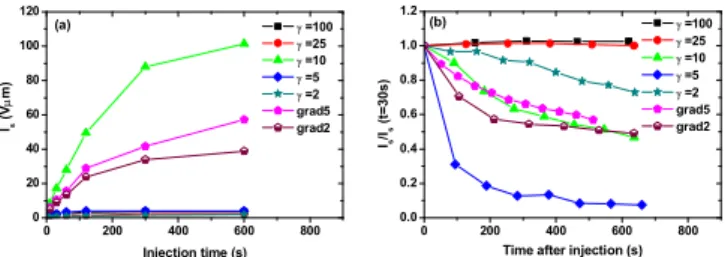
The evolution with charging time of the integrated intensity of potential profiles for bias voltage of 25 V as performed in the KFM study is shown in Fig. 2a for mono-layers with different γ-values and for two nanostructured layers with
continuous levels γ = 100→25→10→5 and γ = 100,
25→10→5→2, called grad5 and grad2. The small integrated
intensity (Is) for the highly insulating layers (γ=100 and 25) is
related to low density of injected charges. The Si-rich layers
(γ=5 and 2) also exhibit small integrated intensity with saturation effect due to increased charge transport in depth of the layer, as well as transversally (the FWHM is doubled). The intermediate layer (γ=10) presents very strong increase of the integrated intensity and fast surface charge diffusion. The two nanostructured layers combine the properties of the constituent layers and behave like insulating layers in terms of charge saturation effect, and like Si-rich layers in terms of charge transport in the volume, however governed by the properties of the intermediate layers with strong surface diffusion.
Fig. 2. Evolution of (a) the integrated intensity, Is for 25 V bias on the AFM
tip, and (b) the Is normalized to its value at 30 s after injection (technological time to start measurements). Charge injection for 5 min at 25 V.
The charge decay mechanisms are also classified according to the layer composition (Fig. 2b). The nanostructured layers follow the decay of intermediate layer revealing simultaneous
action of surface and volume charge transport, however modulated by the presence of other levels in the nanostructure. Combined effect of increased dielectric constant, by increasing the Si-content in the layer, with fast charge decay in the nanostructured layers qualifies them as appropriate for application in capacitive RF MEMS switches.
B. Silica layers with tailored interfaces
Tailoring the properties of a SiO2 layer is achieved by
embedding a single layer of AgNPs (below the percolation threshold) at the vicinity of the dielectric free surface (Fig. 3). The AgNPs are thought to play the role of deep trapping centers thereby stabilizing the charge injection due to the field reduction at the electrode when the AgNPs are charged.
Fig. 3. Bright field TEM images of SiO2 layers with tailored interfaces:
(a) XS-TEM image and (b) PV-TEM image.
Two types of plasma deposits are tested as cover layers:
silica (SiO2) and organosilicon (SiOxCy:H). KFM
measurements of the potential profile induced by charge injection reveal strong lateral charge spreading for the
nanostructure with AgNPs covered by SiOxCy:H layer.
IV. CONCLUSION
Dielectric engineering of thin dielectric layers is applied to establish a new class of nanostructures preventing electrostatic charging. The obtained results show that strong gradual
variation of the conductive properties across the
nanostructured dielectrics provides efficient charge transport in depth of the structure and reduces the electric field at the surface, decreasing in that way the density of injected charges. The presented nanostructured layers appear quite promising for application in RF MEMS capacitive switches.
REFERENCES
[1] C. Laurent, G. Teyssedre, S. Le Roy, and F. Baudoin, IEEE Trans.
Dielectr. Electr. Insul., vol. 20, pp. 357–381, 2013.
[2] T. Tanaka, IEEE Trans. Dielectr. Electr. Insul., vol. 12, pp. 914–928, 2005.
[3] P. Normand et al., Microelectron. Eng., vol. 67–68, pp. 629–634, 2003.
[4] S. Perret-Tran-Van, K. Makasheva, B. Despax, C. Bonafos, P. E. Coulon, and V. Paillard, Nanotechnology, vol. 21, p. 285605, 2010.
[5] G. M. Rebeiz, RF MEMS Theory, Design, and Technology, Hoboken, New Jersy: John Wiley & Sons, Inc., 2003.
[6] W. M. Zhang, G. Meng, and D. Chen Sensors, vol. 7, pp. 760–796, 2007.
[7] N. Tavassolian, M. Koutsoureli, E. Papandreou, G. Papaioannou, B. Lacroix, Z. Liu, J. Papapolymerou, IEEE Transactions on Microwave
Theory and Techniques, vol. 57, pp. 3518-3524, 2009.
[8] K. Makasheva, B. Despax, L. Boudou, and G. Teyssedre, IEEE Trans.
Dielectr. Electr. Insul., vol. 19, pp. 1195–1202, 2012.
[9] A. Pugliara, C. Bonafos, R. Carles, B. Despax,and K. Makasheva,
Material Research Express, vol. 2, p. 065005, 2015.
[10] C. Villeneuve-Faure, K. Makasheva, C. Bonafos, B. Despax, L. Boudou, P. Pons, and G. Teyssedre, J. Appl. Phys., vol. 113, p. 204102, 2013.
0 200 400 600 800 0 20 40 60 80 100 120 γ =100 γ =25 γ =10 γ =5 γ =2 grad5 grad2 Is ( V µ m ) Injection time (s) (a) 0 200 400 600 800 0.0 0.2 0.4 0.6 0.8 1.0 1.2 γ =100 γ =25 γ =10 γ =5 γ =2 grad5 grad2 Is /Is ( t= 3 0 s )
Time after injection (s) (b)