OF TECHNOLOGY
SEP 28 2016
LIBRARIES
-RHNS
M
for Low Power Sensor Interfaces
MASby
[
Frank M. Yaul
B.S. and M.Eng., Massachusetts Institute of Technology (2011)
Submitted to the Department of Electrical Engineering and Computer
Science, Massachusetts Institute of Technology in partial fulfillment of
the requirements for the degree of
Doctor of Philosophy in Electrical Engineering
at the
MASSACHUSETTS INSTITUTE OF TECHNOLOGY
September 2016
2016 Massachusetts Institute of Technology. All rights reserved.
Author ..
. .
Signature redacted
- - - -
W
- -- - - ...
Department of Electrical Engineering and Computer Science
August 31, 2016
Certified by ...
Signature redacted
Anantha P. Chandrakasan
Professor of Electrical Engineering and Computer Science
Thesis Supervisor
Accepted by...
Signature redacted
/
I/s1 A.
Kolodziejski
Professor of Electrical Engineering and Computer Science
Chair, Department Committee on Graduate Students
Amplifier and Data Converter Techniques
for Low Power Sensor Interfaces
by
Frank M. Yaul
Submitted to the Department of Electrical Engineering and Computer Science, on August 31, 2016, in partial fulfillment of the
requirements for the degree of
Doctor of Philosophy in Electrical Engineering
Abstract
Sensor interfaces circuits are integral components of wireless sensor nodes, and im-provements to their energy-efficiency help enable long-term medical and industrial monitoring applications. This thesis explores both analog and algorithmic energy-saving techniques in the sensor interface signal chain.
First, a data-dependent successive-approximation algorithm is developed and is demonstrated in a low-power analog-to-digital converter (ADC) implementation. When averaged over many samples, the energy per conversion and number of bitcycles per conversion used by this algorithm both scale logarithmically with the activity of the in-put signal, with each N-bit conversion using between 2 and 2N+1 bitcycles, compared to N for conventional binary SA. This algorithm reduces ADC power consumption when sampling signals with low mean activity, and its effectiveness is demonstrated on an electrocardiogram signal. With a 0.6V supply, the 10-bit ADC test chip has a maximum sample rate of 16 kHz and an effective number of bits (ENOB) of 9.73b. The ADC's Walden Figure of Merit (FoM) ranges from 3.5 to 20 fJ/conversion-step depending on the input signal activity.
Second, an ultra-low supply voltage amplifier stage is developed and used to create an energy-efficient low-noise instrumentation amplifier (LNIA). This chopper LNIA uses a 0.2V-supply inverter-based input stage followed by a 0.8V-supply folded-cascode common-source stage. The high input-stage current needed to reduce the input-referred noise is drawn from the 0.2V supply, significantly reducing power con-sumption. The 0.8V stage provides high gain and signal swing, improving linearity. Biasing and common-mode rejection techniques for the 0.2V-stage are also presented. The analog front-end (AFE) test chip incorporating the chopper LNIA achieves a power-efficiency figure (PEF) of 1.6 with an input noise of 0.94 PVRMS, integrated from 0.5 to 670 Hz. Human biopotential signals are measured using the AFE. Thesis Supervisor: Anantha P. Chandrakasan .
Acknowledgments
Over these past five years, I've been the recipient of much help, support, and kind-ness, for which I am grateful. I want to thank my advisor, Professor Anantha Chan-drakasan, for encouraging me, challenging me, and helping me to do my best in this thesis work. He has helped me transition into the field, given me a great amount of freedom to explore ideas that interest me, and provided mentorship and guidance over the years. His insights and perspectives on the high-level aspects and broader impacts of projects have been helpful to me, and I hope to continue improving my own understanding in those areas.
I also want to thank my committee members, Professor Harry Lee and Professor Jacob White. I first met Harry as an undergraduate in his recitation section for the introductory-level circuits course, so I owe a great deal of my basic circuits knowledge to his teaching. Over the years he has been helpful and supportive, especially with his analog expertise. I also want to thank Jacob for his enthusiasm and resourcefulness, which I was able to witness first hand while helping out with a class he taught. I want to thank him for discussing issues related to low-power classifiers with me.
Several sources of funding have supported this thesis work. I want to thank the Department of Defense's Science and Engineering Graduate Fellowship Program, which provided the initial funding while the course of this thesis work was being set. I want to thank Shell and Texas Instruments, who sponsored and lended expertise to the industrial microsensors project. I also received support from Delta Electronics towards towards the end of this thesis work. Finally, I'm especially grateful the Taiwan Semiconductor Manufacturing Corporation for fabricating both test chips through the University Shuttle Program.
I've thoroughly enjoyed working alongside many fellow students throughout my time at MIT. Michael, thanks for helping me in many ways, from troubleshooting issues on the lab bench to teaching me about speech recognition. Marcus, thank you for sharing your time and analog expertise with me. You've directly helped me with both projects in this thesis, and I've learned so much from your work. Sungjae, it
was an honor sharing a cube with you. You've shown great patience and kindness even when things were busy and you were balancing being a father, husband, and researcher. Arun and Nathan, thanks for always being eager to help, and for your involvement in the microsensors project. Sirma, Harneet, and Taehoon - thanks for your camaradarie as fellow amplifier and data converter students. Finally, to everyone in Anantha's group -you make lab a place I enjoy working in. I'm thoroughly grateful to have met each of you. Also, Jennifer and Professor Yury Polyanskiy - I wish I had more time to work with both of you. Thanks for all the interesting ideas you've shared with me.
I am grateful to my friends from the MIT Graduate Christian Fellowship, who have been with me in both the fun times of research as well as the challenging times, supporting me in many ways. Ming, Yukkee, Po-Ru, Charis, Kunle, Alex, Becky, Peng, and Annie - thanks for all the advice and care you've given me over the years. I'm grateful for being able to befriend and learn from people a few steps ahead in life. Gerald, Hosea, Megan, Madeline, and Alice - thanks for walking alongside me over these past few years. I'm grateful for the time we've spent together. Ronny, you fit somewhere in between those two groups. You've been both a mentor and a peer, and you always take the time to help me.
I'm also very fortunate to have several friends who have gone through MIT with me for undergrad and then stayed at MIT for varying amounts of graduate school. Steve, it's been an honor being your friend all these years. From playing in the pit orchestra of Next Act, to being roommates in Sidney-Pacific, to going on a run while discussing algorithms for Boggle, our adventures have taken many forms. Gabriel, thanks for being a mentor and a friend to me. You've shown great kindness to me and gone out of your way to look out for me on many occasions. Andrew and Peter, thanks for your friendship. It's always good to bump into you guys on campus.
Mom and Dad, thanks for always being there for me. You've selflessly supported me and cared for me all these years, and you've been a constant in all the transitions throughout my life. Thanks for encouraging my interest in science. Finally, I thank God for the grace, guidance, provision, and spirit which have brought me to this
point. Whether the times are fun or challenging, I will try my best, knowing that there is something good to be done in any time. Thank you Lord for everything.
Everyone, many thanks - it has been a journey. I hope the ideas introduced in this thesis will be both interesting and useful to you.
If I take the wings of the morning
and dwell in the uttermost parts of the sea, even there your hand shall lead me,
and your right hand shall hold me. If I say, "Surely the darkness shall cover me,
and the light about me be night," even the darkness is not dark to you;
the night is bright as the day, for darkness is as light with you.
Contents
1 Introduction
1.1 Background ... .. .. ... .. .. 1.1.1 Biopotential Monitoring . . . . 1.1.2 Vibration Monitoring . . . . 1.1.3 Strain, Pressure, and Temperature Sensing 1.1.4 Voice Activity Detection . . . . 1.1.5 Sum mary . . . . 1.2 Research Goals and Contributions . . . . 1.3 Thesis Organization . . . . 2 LSB-First Successive Approximation
2.1 Introduction . . . . 2.2 LSB-first Successive Approximation . . . . 2.2.1 Algorithm Description . . . . 2.2.2 Algorithm Details . . . . 2.3 Algorithm Simulation and Comparison . . . . 2.3.1 Fundamental Limits of Bitcycle Reduction 2.4 ADC Circuit Design . . . . 2.4.1 Capacitive DAC . . . . 2 .4.2 DAC Switches . . . . 2.4.3 Dynamic Comparator . . . . 2.4.4 Low-leakage Bitcycling Logic . . . . 2.4.5 Top-Level Simulation and Verification . . .
23 24 26 28 29 30 30 31 32 35 . . . . 36 . . . . 38 . . . . 39 . . . . 42 . . . . 43 . . . . 45 . . . . 47 . . . . 47 . . . . 54 . . . . 59 . . . . 61 . . . . 63
2.5 ADC Performance Measurement . . . . 65
2.5.1 DNL and INL . . . . 67
2.5.2 Spectral Measurements . . . . 70
2.5.3 Power Consumption, Sample Rate and Voltage Scaling . . . . 71
2.6 Data-Dependent Energy Savings . . . . 74
2.6.1 Logarithmic Power Scaling . . . . 74
2.6.2 Test Case: Electrocardiogram Input Signal . . . . 76
2.6.3 Slope-based Prediction . . . . 77
2.7 Conclusion . . . . 78
3 A Noise-Efficient Multi-Voltage Instrumentation Amplifier 81 3.1 Introduction . . . . 82
3.2 Noise and Power Consumption Trade-offs . . . . 84
3.3 Noise-Efficient Multi-Voltage Amplifier . . . . 86
3.3.1 0.2V Squeezed-Inverter Input Stage . . . . 89
3.3.2 0.8V Folded-Cascode Common-Source Stage . . . . 91
3.3.3 Feedback, Chopping, and CMR Scheme . . . . 92
3.3.4 Stability Analysis . . . . 94
3.3.5 Interferer Rejection Analysis . . . . 96
3.3.6 Noise Analysis . . . . 98
3.3.7 Negative Gate Bias Generation . . . . 100
3.4 AFE Implementation . . . . 105
3.4.1 Chopper LNIA Details . . . . 105
3.4.2 Chopper OTAs . . . . 109
3.4.3 PGA and AA Filter . . . . 110
3.4.4 Buck Converter . . . . 112
3.4.5 Current and Voltage References . . . . 113
3.4.6 Simulation and Verification . . . . 114
3.5 AFE Performance Measurements . . . . 116 3.5.1 Transfer Functions, Noise and Step Response . . . .1 119
3.5.2 Input Impedance ... 3.5.3 Nonlinearity. .. ... . . . . 3.5.4 Buck Converter . . . . 3.5.5 Temperature Stability . . . . 3.5.6 Voltage Scaling . . . . 3.5.7 Performance Summary . . . . 3.6 Biopotential Measurements . . . . 3.7 C onclusion . . . . 4 Methods for Low-Power Event Detection
4.1 D ecision Trees . . . . 4.2 Feature Extraction . . . . 4.3 Classifier-based Analog Performance Scaling . . . . 4.4 Modeling Noise in Feature Vectors . . . . 4.5 C onclusion . . . . 5 Conclusion
5.1 Summary of Contributions . . . . 5.2 Directions for Future Research . . . . A List of Acronyms
B Shot Noise Power Spectral Density References 121 121 123 124 125 125 127 129 131 132 133 134 135 137 139 142 142 145 149 151
List of Figures
1-1 Circuit blocks comprising a typical wireless sensor node. This thesis explores circuit and algorithmic techniques to reduce power consump-tion in the three highlighted blocks. . . . . 24 1-2 23-channel EEG recording from a pediatric subject experiencing an
epileptic seizure from 27s to 54s. Vertical scale is 500 pV/tick. EEG channels are labeled according to the International 10-20 system. The plots were generated from the PhysioNet chbO1_04 dataset [1, 2]. . . 27
1-3 Vibration power spectral density (PSD) of a roller bearing during nor-mal operation and after a roller element fault. The shaft rotation speed was fixed at 2000 RPM. The plots were generated using the Bearing dataset from the NASA Ames Prognostics Data Repository [3, 4]. . . 29
2-1 Sensor signals with low activity factor a. Top: ANSI/AAMI EC13 test ECG waveform [5] sampled at 720 Hz and 12b resolution. Bottom: Roller bearing vibration data [3, 4] sampled at 20 kHz and scaled to 1/4 fullscale amplitude at 10b resolution. . . . . 37 2-2 Example 10-bit conversions using the LSB-first SA algorithm. Fewer
bitcycles are needed when the initial guess is more accurate. The break in the vertical axis indicates that only a small portion of the 10-bit fullscale range is shown. Only D[4: 0] are shown in the timing diagram because D[9 : 5] are never altered by the algorithm in this example. The bolded binary digits in the table indicate the current bit under test. 39
2-3 Flowchart illustrating LSB-first successive approximation. The com-parator outputs 1 when VDAC > VIN .. . . . . . . .. . . 40
2-4 P1, the INIT phase, uses 1 to 2 bitcycles to determine the error di-rection of the initial guess of DPREV. VLB and VUB are the upper and lower code bound voltages of the guess. Each branching point indicates a comparison performed between VDAC and VIN- -..-... -...41
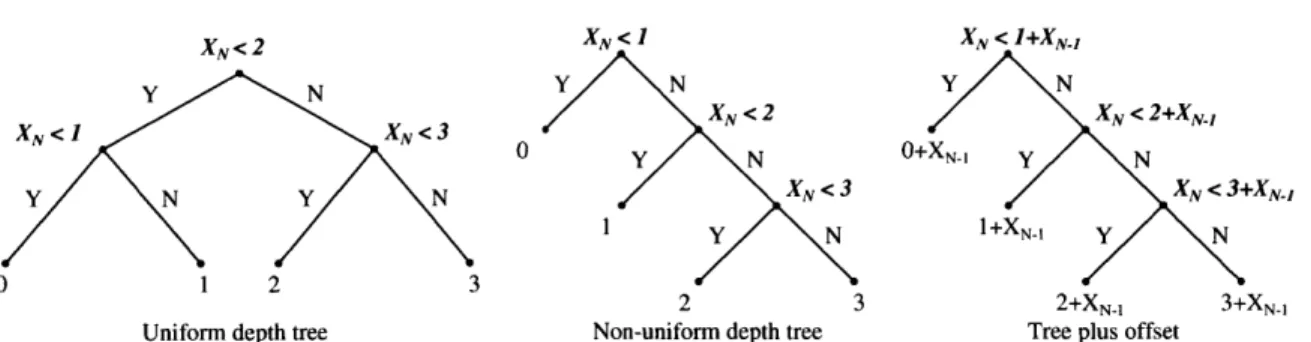
2-5 Simulated mean bitcycles/sample plotted against mean Acode for fullscale sinusoid inputs of different frequencies. Different lines represent differ-ent SA algorithms. The top plot compares LSB-first SA to conven-tional SA. The bottom plots compare LSB-first SA to the algorithms described in [6] and [7]. . . . . 44 2-6 Different successive approximation search trees for 2-bit search. XN is
the current sample and XN-1 is the previous sample. . . . . 45 2-7 LSB-first SA is simulated and compared to H(AX) for fullscale
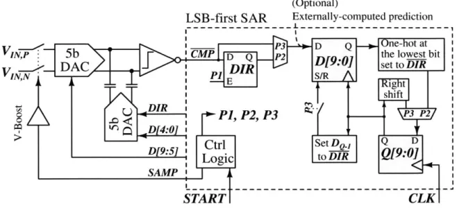
sinu-soid inputs of different frequencies as in Figure 2-5. Note that H(AX) can be greater than 10 bits because AX has double the range of X ( 1023 codes). . . . . 46 2-8 Architecture of the LSB-first SAR ADC showing the main analog and
digital blocks. . . . .. . . . 47 2-9 Conversion timing diagram showing main control signals and number
of clock cycles per phase. . . . . 48 2-10 Schematic of the differential 10-bit capacitive DAC comprising 5-bit
DACs capacitively coupled to 5-bit sub-DACs. . . . . 48 2-11 Single-ended DAC schematic illustrating Thevenin equivalents of the
main- and sub-DACs. Top-plate parasitic capacitances Cp are also show n . . . . 49 2-12 Single-ended capacitive DAC layout showing common-centroid
place-ment and dummy devices labeled D. Note that CC and CD denote the coupling capacitor and the DIR capacitor, respectively . . . . 52
2-13 Schematic of the voltage-doubling charge pump used to drive top- and bottom-plate NMOS sampling switches . . . . 55 2-14 DAC bottom-plate switch network. Left to right: Bitcycling switches,
purging switch, and sampling switches. . . . . 56 2-15 Asymmetric PMOS and NMOS reference switch resistance may cause
VDAC to momentarily dip below ground, resulting in potential charge loss. . . . .. . . . 57 2-16 Current paths for top-plate switch charge vary significantly
depend-ing on whether the bottom-plate sampldepend-ing switches are on or off, as depicted in [8]. . . . . 59 2-17 Schematic of the two-stage dynamic comparator, including the output
S-R latch . . . . 60 2-18 Transient simulation of dynamic comparator internal node voltages
with a 0.6V supply and VINP = 299 mV and VINN= 301 mV. .... 60 2-19 Simulated fraction of comparisons resulting in CMP = 1 plotted
against input offset. The manually-fitted normal CDF has 1 = 0.02 mV and o-= 0.16 mV. . . . . 61 2-20 Detailed LSB-first SAR logic. Compare to Figure 2-8. The middle 3
bits of the 10-bit implementation are shown. . . . . 62 2-21 Simulated energy per sample of the full chip including extracted
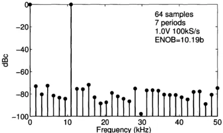
para-sitics and the padring. Test cases include 2-bitcycle and many-bitcycle cases for both 1.OV/45OkSps and 0.6V/16kSps configurations. .... 63 2-22 FFT plot of simulated output codes yielding 10b ENOB. 64 samples
of exactly 7 periods of an input fullscale sinusoid were taken. . . . . . 64 2-23 LSB-first SAR ADC chip micrograph. . . . . 65 2-24 LSB-first SAR ADC testbench diagram. . . . . 66 2-25 LSB-first SAR ADC testbench photograph taken during the ECG test
with a sense resistor and differential amplifier to measure the power consumption waveform. . . . . 67
2-26 DNL/INL measurement results using DPREV as the initial guess. VDD=1V and fs= 100 kHz. . . . . 68 2-27 Quantization boundaries for output codes 0 to 9 shown for different
values of DIR. The example non-uniform code widths are exaggerated to show how the DNL of the two configurations is related. . . . . 69 2-28 Comparison of DNL/INL measurements using previous sample as the
initial guess (black) and using code 511 as the initial guess (red).
VDD=1V and fs=100 kHz. . . . . 69 2-29 Top: Measured ADC output spectra at VDD=0.6 V and fs=16 kHz
for both low and high frequency inputs. Bottom: SNDR and SFDR versus input frequency at different supply voltages and sample rates. . 71 2-30 Sample rate versus power measurement at different supply voltages,
given a DC input voltage. . . . . 72 2-31 Measured maximum fs, SNDR, SFDR, and FoM for different supply
voltages. The frequency of the fullscale sinusoid test input is scaled proportionally to the sample rate used. . . . . 72 2-32 Measured power consumption of each component of the ADC at a 10
kHz sample rate. The measurement was taken at two supply voltages for both low and high frequency fullscale sinusoid inputs. . . . . 74 2-33 Measured mean bitcycles/sample and mean energy consumption at
fs = 10 kHz and VDD = 0.6V as a function of mean output code change per sample, for differently-shaped inputs. . . . . 75 2-34 Measured LSB-first SAR ADC response to slow-varying 5 Hz fullscale
sinusoid, showing number of bitcycles/sample alongside the input wave-form, and a histogram of the bitcycle/sample count. The ADC was operated at 10 kS/s with a 0.6V supply. . . . . 76 2-35 ADC response to ECG test input signal with fs = 1 kHz and VDD =
0.5V, demonstrating the ADC's low leakage and data-dependent energy consum ption. . . . . 77
2-36 The varying-frequency fullscale sinusoid experiment of Figure 2-33 is repeated using slope-based prediction . . . . 78 3-1 Power budget of a wireless sensor node following the biosensor example
of
[9].
The system continuously monitors a signal and transmits featurevector data to a basestation. Approximate figures of merit are taken from [10, 11, 12, 13] and are scaled to the listed performance to obtain the power numbers. . . . . 82 3-2 MOSFET drain current noise PSD. . . . . 84 3-3 Supply voltage requirements for various amplifier input stage topologies. 87 3-4 Supply voltage requirements for the proposed squeezed-inverter
topol-ogy capable of 2VDSAT (0.2V) operation. . . . . 87
3-5 Multi-voltage LNIA concept comprising a 0.2V inverter-based input stage followed by a 0.8V folded-cascode common-source stage. .... 88 3-6 Plot of VDDL supply voltage vs. theoretically achievable gain of a single
squeezed-inverter stage. . . . . 90 3-7 Folded-cascode common-source (FCCS) stage used in the LNIA (left)
and CMFB implementation (right). . . . . 91 3-8 Block diagram of the single-ended half-circuit of the fully differential
Multi-Voltage LNIA. Choppers are represented by crossed rectangles. 92 3-9 Simplified schematic and frequency response of a typical two-stage
op-amp using Miller compensation. . . . . 94 3-10 Simulated DM loop transfer function of the overall LNIA including
the capacitive feedback network using Spectre PSTB analysis on the schem atic. . . . . 96 3-11 Simulated CMR loop transfer function using Spectre PSTB analysis
on the schem atic. . . . . 97 3-12 Simulated LNIA transfer function and input-referred noise using
Spec-tre PNOISE analysis on the schematic. . . . . 100
3-14 Feedback block diagram for analyzing the negative gate bias generator's noise sources. . . . . 102 3-15 Simplified schematic for analyzing the negative gate bias generator's
stability. . . . . 102 3-16 Simulated negative gate bias loop transfer function using Spectre PSTB
analysis on the schematic. . . . . 103 3-17 Simulated negative gate bias noise PSD using Spectre PNOISE analysis
on the schem atic. . . . . 104 3-18 System block diagram of the noise-efficient sensor AFE chip. . . . . . 104 3-19 Schematic showing additional implementation details of the chopper
L N IA . . . . 106 3-20 Simplified schematic for stability analysis of the input
impedance-boosting PFL. . . . . 107 3-21 Schematic modeling the effect of Co on chopping spikes induced by CL. 108 3-22 Cascode bias voltage generation technique. . . . . 108 3-23 Single-stage folded-cascode chopper (SSFCC) amplifier used in the
bi-asing loops and reference buffers. . . . . 109 3-24 Single-ended version of the PGA showing variable-gain capacitive
feed-back network with unit capacitor size C of 0.5 pF. The switches are configured in 8x gain mode with PG[1:0]= 11. . . . . 110 3-25 Schematic of the core amplifier used in the PGA. The same topology
is used in the AA filter. . . . . 111 3-26 Buck converter using PFM regulation and off-chip LC and RCRC filter
netw orks. . . . . 112 3-27 Widlar current reference with fast-startup modifications described in
[14 ]. . . . . 1 13 3-28 Half-VDD reference generators. . . . . 114 3-29 Micrograph of the sensor AFE test chip . . . . 116 3-30 Diagram of the LNIA testbench. . . . . 117
I
3-31 Photograph of the LNIA testbench during an early iteration of an experiment measuring the LNIA's performance while using the buck
converter to power the 0.2V input stage. . . . . 118 3-32 Schematic of the LNIA testbench's input resistor attenuation network. 118 3-33 Measured AFE transfer functions and output noise vs. frequency. . . 119 3-34 Measured step response in the presence of a large common-mode
in-terferer. The offset in the input waveforms is primarily due to the oscilloscope. . . . . 120 3-35 Measured THD vs. output amplitude using a 100Hz test tone. . . . . 121 3-36 Measured percent nonlinearity of a 75%-fullscale tone versus input AC
common-mode amplitude. . . . . 122 3-37 Measured output spectrum of the AFE test chip given an input with
a 117 Hz DM tone combined with 100 Hz CM tone. . . . . 122 3-38 Measured buck converter drain and filtered output waveforms. . . . . 123 3-39 Measured performance and bias current vs. temperature. . . . . 124 3-40 Measurements showing the effect of VDDL scaling on bias current and
noise efficiency. . . . . 125 3-41 Schematic of AC coupling and LPF network used to interface with the
electrodes. . . . .. . 127 3-42 Diagram of biopotential electrode placement and photograph of EEG
electrodes . . . . 128 3-43 Photograph of EEG electrodes and headband on the test subject. . . 128
3-44 Lead III ECG measurement taken using the AFE test chip. . . . . 128 3-45 Visual cortex EEG measurement taken using the AFE test chip. . . . 129
4-1 Decision boundaries of different types of classifiers. . . . . 132 4-2 Block diagram of feature extraction process as used in
[15].
. . . . 134 4-3 Top: Histogram of a feature band magnitude squared, given a whitenoise input. Bottom: Mean and variance of histogram frequency band feature magnitude squared vs. input noise power. . . . . 136
List of Tables
1.1 Low-power wireless sensor node applications. . . . . 26 1.2 Power consumption of the front-end amplifier and data converter in
various micro- and nano-power sensor node applications. . . . . 31 2.1 Main-DAC capacitor area and edge counts . . . . 53 2.2 Summary table comparing this work with other recent 10b low-leakage
SAR ADC designs. . . . . 79 2.3 Performance variation over 10 test chips. SNDR/SFDR test conditions:
0.6V supply, 16 kS/s, 337 Hz input tone. The FoM was computed using the near-DC power consumption and the 337 Hz ENOB. Note: Later measurements showed smaller offset magnitude than the original measurements reported here which did not account for signal generator offset. . . . . 80 3.1 Transfer function parameters used in the LNIA design. AINV is
esti-mated as 20x in these calculations. . . . . 95 3.2 PGA gain modes and feedback capacitances as a function of unit
ca-pacitance C . . . . 110 3.3 Schematic simulations of full chip design across process corners. Unless
specified, simulations were performed for room temperature (27'C) and the 800x gain mode. . . . . 114 3.4 Summary table comparing this work with other recent power-efficient
Chapter 1
Introduction
Applications of wireless sensor nodes (WSNs) range from complex tasks such as target tracking and node localization, to simple tasks such as continuous signal monitoring and event detection. This thesis focuses on micro- and nano-power event detection applications where radio transmissions are infrequent and the sensor interface is a significant component of the system's power consumption. Such applications include vital signs monitoring for medical condition detection, vibration and strain sensing for machine and building health monitoring, and temperature and moisture sensing for precision agriculture. In these applications, instead of continuously transmitting sensor data to a basestation, low power signal processing and event detection is per-formed on the sensor node and data is only transmitted during an event of interest. In contrast, the sensor interface and event detection algorithms must operate con-tinuously. This motivates the work in this thesis to improve the energy-efficiency of sensor interfaces.
This thesis aims to improve the energy-efficiency of sensor interfaces through both circuit- and algorithm-level techniques. Figure 1-1 depicts the circuit blocks used in a typical WSN, and shows the areas that this thesis focuses on. A typical WSN must interface with the sensors, condition and digitize the sensor signals, and perform dig-ital signal processing (DSP) to reduce the data before transmission. Work in this thesis comprises two projects covering different parts of the signal chain. The first project, detailed in Chapter 2, develops a data-dependent search algorithm to reduce
Typical WSN
Energy DC-DCharvester Converter Energy Sstorage
Sensor AFE A ADC - DSP RF
Thesis Contributions
VH1Vc VIN
+ A, A2
VDAC
Efficient low-noise A/D conversion using
signal amplification a data-dependent
search algorithm
Figure 1-1: Circuit blocks comprising a typical wireless sensor node. This thesis explores circuit and algorithmic techniques to reduce power consumption in the three highlighted blocks.
the conversion energy of an ADC and includes the design and testing of a chip imple-mentation. The second project, detailed in Chapter 3, involves designing and testing a low-noise instrumentation amplifier (LNIA) that uses a 0.2V-supply input stage to achieve a high noise-efficiency. The LNIA is used in an analog front-end (AFE) to create a high-impedance sensor interface. Finally, a discussion of current algorithms for low-power event detection is included in Chapter 4. Methods of relaxing AFE performance based on the requirements of the event detector provide the potential for significant energy savings.
1.1
Background
A typical WSN comprises a radio transceiver, sensors, sensor interfaces, an embedded
processor, and energy harvesting and management circuits. Together, these mod-ules enable remote, long-term monitoring of various sensor signals of interest.
Spe-cific applications include biopotential sensing for diagnosis and detection of medical conditions, vibration sensing for fault detection in industrial plant machinery, and temperature and strain sensing for building monitoring. Sensors range from pas-sive biopotential electrodes, piezoelectric accelerometers, and electret microphones, to active pixel arrays and ultrasonic transducers.
The WSN's sensor interface typically includes a front-end amplifier directly con-nected to the sensor. The amplified output is then sent to an ADC. A digital back-end (DBE) then extracts features from the data stream, reducing the quantity of data. At this point, higher-power sensor nodes may wirelessly transfer the reduced data to other nodes, allowing for data aggregation and array processing. However, in applications with greater energy constraints, frequent data transmission and com-plex processing on the node may not be feasible. Instead, low-power WSNs may be designed for entirely local data processing, and may only transmit sensor data during an event of interest in order to achieve further power savings. For example, an implanted biomedical device may be configured to detect an alarm condition in a patient's vital signs. Upon detection, the sensor node can proceed to alert the basestation and transmit relevant sensor data. In these event-detection applications, high-level data processing performed locally in the WSN allows RF transmission to be limited to significant events. In alarm-type applications where the event is relatively rare (< 1/hour), the average power consumption of the RF block may be reduced be-low that of the always-on LNIA, ADC, and DSP blocks. A recent work
[13]
showcases an RF transmitter that can be duty-cycled to sub-nW power consumption levels.To realize "detect-and-alert" capability on a sensor node, a low-power method of continuously monitoring signals and detecting events of interest is required. Though some applications may employ active sensors with significant power consumption, many applications make use of passive sensors which draw very little or no power at all. Additionally, tools from the fields of machine learning and statistics have been successfully used in a number of event detection applications, using low-power feature extraction combined with computationally cheap linear classifiers or decision trees (DTs). Recent work includes a 0.1 pW 7-band FIR filter bank for spectral feature
Application Sensor Signal feature Event of interest
ECG-based Biopotential Heart rate Arrhythmia
arrhythmia detection [16] electrode
EEG-based Biopotential EEG spectrum Epileptic seizure
seizure detection [12] electrode
Vibration Piezoelectric Vibration Machine fault
monitoring [17] accelerometer spectrum
Structural Strain gauge DC level Structural fault
monitoring [18]
Voice activity Passive Sound spectrum Speech presence
detection
[19]
microphonePrecision Temperature, DC level Irrigation required
agriculture [20] moisture
Table 1.1: Low-power wireless sensor node applications.
extraction from electroencephalogram (EEG) signals [12] and a 6 PW voice-activity detection (VAD) system employing detection algorithms of varying complexity and power, ranging from a threshold-based wake-up detector to a DT classifier [19]. Ta-ble 1.1 lists several WSN applications where detect-and-alert functionality may be used to limit radio transmissions while still allowing the node to respond to events of interest.
With the power of the DBE and radio greatly reduced through the use of low-power event detection techniques, the low-power of the WSN's sensor interface becomes more significant, in part because it must be always-on to continuously monitor the sensor signals. The increasing significance of the sensor interface's power consumption motivates further investigation into energy-efficient amplifiers and data converters for these detect-and-alert applications. Current work in the area of low-power sensor interface circuits includes many application-specific analog front-ends (AFEs) which are discussed in the following sections.
1.1.1
Biopotential Monitoring
Biopotentials such as the electrocardiogram (ECG) and the electroencephalogram (EEG) are used by physicians to diagnose conditions including heart disease, sleep disorders, and epilepsy. Recently, interest in preventative medicine has spurred the
T81P8 FT 0T103 0 06 08 FT9FT10 T7FT9 P7T7 CZPZ FZCZ P802 T8P8 F8T8 FP2F8 P402 C4P4 F4C4 FP2F74 P301 C3P3 F3C3 FP1F3 P701 T7P7 F7T7 FP1F7 0 10 20 30 40 50 60 70 80 Time (s)
Figure 1-2: 23-channel EEG recording from a pediatric subject experiencing an epilep-tic seizure from 27s to 54s. Verepilep-tical scale is 500 pV/epilep-tick. EEG channels are labeled according to the International 10-20 system. The plots were generated from the PhysioNet chbOK0O4 dataset [1, 2].
development of wearable electronic health monitoring devices with the goal of long-term continuous monitoring of patient vital signs and biopotentials. The data gen-erated from these devices grants doctors information about the patient not possible to obtain during a, single visit, and also allows patients to monitor their own health, assisting them in setting measurable goals for improvement. Current research in the area of patient health monitoring aims to increase the node's capability to interpret the raw sensor data while also further reducing the node's power consumption. These
two thrusts improve the viability of long-termi patient monitoring.
EEG-based seizure detection is one biomedical sensor node application of inter-est to researchers due to the large amount of sensor data that must be acquired and interpreted, as shown in Figure 1-2. The dimensionality and rate of the data nmay be significantly lowered through feature extraction of frequency band energies, greatly reducing the processing load and power consumption of the back-end classifier. In contrast, since each channel requires its own LNIA, the total analog power con-sumption becomes a power bottleneck [12]. Examples of current work in low-power
biomedical sensor interfaces includes improvements to the basic amplifier and data converter circuits with a focus on improving the tradeoff between power consump-tion and noise/resoluconsump-tion [21, 22] and increasing interferer rejecconsump-tion capability in the front-end amplifier [23].
In addition to block-level circuit innovations, many system-level techniques have emerged in response to the variety of applications in the field of biomedical sensors. Analog and mixed-signal techniques have yielded low-power implementations of vari-ous signal processing and filtering functions [24, 25]. For applications with lower SNR requirements, an analog approach to signal processing can be more energy-efficient than a predominantly digital one [26]. Biomedical sensor interfaces have also benefit-ted from developments in compressed sensing which has been used in a photoplethys-mography system to reduce active sensor power [27], and machine learning which has been used in low-power Systems-on-Chip (SoCs) to detect epileptic seizures from EEG data [12, 28]. Additionally, AFE and DSP co-design has led to the creation of a 64 nW syringe-injectable implant using the ECG to detect heart arrhythmias [16]. Significant power savings were achieved by relaxing the noise performance of the implant's AFE to the minimum level needed to maintain arrhythmia detection accuracy. A 3 nW, 370 Hz bandwidth signal acquisition system comprising an ampli-fier and ADC [29] further demonstrates the power reduction that results from relaxed noise specifications.
1.1.2
Vibration Monitoring
Accelerometers are widely used to monitor the vibration spectra of industrial ma-chines in order to detect faults early on, enabling preventative maintenance [17]. The frequency of spurs in the measured vibration power spectral density (PSD) can be matched with knowledge of the machine's mechanical components in order to deduce the location of the fault. For example, a gear with a defect on one of its k teeth would result in a spur at the kth harmonic of the rotation frequency, and the roller element of a bearing can produce a spur at twice its rolling frequency as it contacts both the inner and outer race. Figure 1-3 shows the change in a vibration PSD measured
10 10
A
'N i l9Fault 10-2 1 10-3 Normal 10 4 ' '- - 1 0 1 2 3 4 5 6 7 8 9 10 Frequency (kHz)Figure 1-3: Vibration power spectral density (PSD) of a roller bearing during normal operation and after a roller element fault. The shaft rotation speed was fixed at 2000 RPM. The plots were generated using the Bearing dataset from the NASA Ames Prognostics Data Repository [3, 4].
from an accelerometer mounted on the bearing's outer housing. Outlier detection algorithms [30] or machine learning techniques [31] may be used to detect and report changes in a machine's vibration spectrum.
Piezoelectric accelerometers are commonly used because they do not require an external power source and are capable of withstanding high temperatures and accel-erations. Their lack of a DC response is not an issue for vibration sensing. However, because a piezoelectric sensor is inherently a charge-output device, the sensor inter-face must be designed accordingly. As with biopotential sensor interinter-faces, a piezo-electric sensor interface comprises a low-noise amplifier and an ADC. However, a transimpedance amplifier (TIA) may be used instead of an LNIA because the TIA's virtual-ground input prevents cable capacitance from loading the piezoelectric ele-ment.
1.1.3
Strain, Pressure, and Temperature Sensing
"Near-DC" signals, such as those from strain, pressure, and temperature sensors vary over the course of minutes to days, so the sensor interface must have a DC response, unlike in biopotential or vibration monitoring applications. However, as the bandwidth of the sensor interface is scaled down to match the application's low data rate, the overhead power consumption of peripheral circuits such as current references
becomes more significant, making it difficult to achieve linear power scaling with data rate. Therefore, instead of focusing on further reductions in power consumption, one recent work in the area of strain sensing aims to expand the sensor node's capability to enable strain monitoring with high spatial resolution over a large area [18]. This capability may be used to detect faults in buildings so that proper maintenance may be performed. The strain monitoring system uses thin-film transistors on a flexible substrate to provide a dense, active strain-sensing array, while CMOS devices are used to demodulate and digitize the sensor output signals.
1.1.4
Voice Activity Detection
Natural language interfaces enable intuitive control and interaction with energy-constrained embedded devices and WSNs. Speech signals may be transduced us-ing electret microphones, which use a permanently-charged dielectric diaphragm and therefore do not inherently require an external power supply. Unfortunately, the power requirements of running a high-accuracy speech decoder with a high-performance microphone AFE are prohibitive. Low-power voice-activity detection (VAD) capabil-ity is a solution to this issue that allows the WSN to remain in a low-power mode until speech is detected. Current work in micropower VADs includes an energy threshold-ing detector combined with a mixed-signal DT classifier [19]. The energy thresholdthreshold-ing is performed with low-power a preamplifier and a comparator, consuming 0.71 pW in total. When the threshold is exceeded, an analog filter bank extracts frequency band features which are fed into the DT classifier. The analog feature extraction and DT consume up to 6 pW. Since most of the lifetime of the embedded device or WSN is spent in its low-power mode, reducing the energy of the VAD to the microwatt level greatly extends the device's battery lifetime.
1.1.5
Summary
The aforementioned case studies of different low-power sensor interface circuits show the potential utility of WSNs and motivate continued efforts to improve their
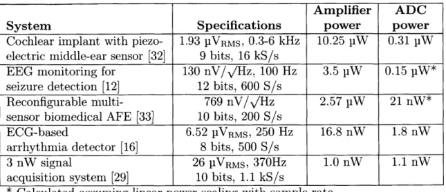
per-Amplifier ADC
System Specifications power power
Cochlear implant with piezo- 1.93 PVRMS, 0.3-6 kHz 10.25 pW 0.31 pW electric middle-ear sensor [32] 9 bits, 16 kS/s
EEG monitoring for 130 nV//Hz, 100 Hz 3.5 pW 0.15 pW* seizure detection [12] 12 bits, 600 S/s
Reconfigurable multi- 769 nV/i/Hz 2.57 pW 21 nW*
sensor biomedical AFE [33] 10 bits, 200 S/s
ECG-based 6.52 PVRMS, 250 Hz 16.8 nW 1.8 nW
arrhythmia detector [16] 8 bits, 500 S/s
3 nW signal 26 l1VRMS, 370Hz 1.0 nW 1.1 nW acquisition system [29] 10 bits, 1.1 kS/s
* Calculated assuming linear power scaling with sample rate.
Table 1.2: Power consumption of the front-end amplifier and data converter in various micro- and nano-power sensor node applications.
formance and reduce their power consumption. Many applications use a straight-forward combination of a low-noise front-end amplifier followed by an ADC, while other applications using active sensors requiring additional demodulation and signal conditioning. Also, because most sensor signals are slow, the amplifier and data con-verter must be capable of operating efficiently at low bandwidth and data rates. In long-term continuous monitoring applications, the power efficiency of the always-on sensor interface circuits is critical to extending node lifetime. The power breakdown between the front-end amplifier and the data converter in several micro- and nano-power sensor node applications is shown in Table 1.2. Overall, though there are a variety of requirements on the amplifier and ADC imposed by different applications, improvements in the performance and power efficiency of these basic circuit blocks have the potential to benefit many sensor systems.
1.2
Research Goals and Contributions
The goal of the research in this thesis is to explore both circuit- and algorithm-level techniques to improve the energy-efficiency of components of the sensor interface signal path. This research aims to be generally applicable to various types of sensors, but also strives to be sufficiently grounded in the well-studied sensor node applications
of medicine and industry. The techniques developed in this thesis are used to design a proof-of-concept data converter and amplifier targeting low-bandwidth sensor signals. The following list includes key contributions of this thesis to the field of low-power sensor interface circuits:
" Developed a data-dependent successive approximation (SA) algorithm called LSB-first SA which converges faster than conventional binary search when given a good initial guess of the conversion result. Demonstrated that the average convergence time scales logarithmically with the average error in the initial guess.
* Designed an efficient hardware implementation of LSB-first SA requiring mini-mal additional combinational logic and no extra registers per bit compared to conventional SAR logic.
" Demonstrated performance benefits of LSB-first SA on an ADC test chip sam-pling a test ECG signal using the previous sample as the initial guess for the current sample's value.
" Developed a multi-voltage LNIA technique combining the noise-efficiency of a 0.2V input stage with the gain and signal swing of a 0.8V cascode stage, while using feedback to linearize the overall amplifier. Developed biasing and interferer rejection techniques for the 0.2V stage.
" Designed a complete AFE integrating the LNIA with supporting circuitry. Demonstrated the test chip's ability to achieve a high PEF while having suffi-cient linearity, bandwidth, and interferer rejection to transduce both ECG and EEG biopotential signals.
1.3
Thesis Organization
Chapter 2 presents the LSB-first SAR ADC, beginning with a description of the data-dependent search algorithm. Algorithm-level simulation results are presented and
compared to other data-dependent search techniques in the literature. The schematic-level circuit design is explained, and layout techniques for the capacitive DAC are shown. Test chip measurement results are presented and discussed. The chapter concludes by summarizing contributions and providing directions for future work.
Chapter 3 details the low-voltage LNIA. The chapter begins by motivating supply voltage reduction as a method of improving noise-efficiency. The 0.2V-supply input stage is introduced and the multi-voltage LNIA concept is explained and analyzed. The overall architecture of the complete AFE test chip is presented, and circuit de-sign details are explained. Finally, test chip measurement results are presented and discussed. Contributions are reviewed and directions for future work are suggested.
To complement the low-power ADC and amplifier techniques presented in this the-sis, Chapter 4 discusses some existing low-power algorithms for implementing event detection. Decision Tree (DT) classifiers are considered due to their minimal hard-ware requirements. Algorithms to scale the performance of the AFE based on the requirements of the classifer are highlighted.
Chapter 5 concludes the thesis and discusses additional possible applications for the ideas presented in this thesis as well as directions for future research.
Chapter 2
LSB-First Successive
Approximation
This chapter presents a successive approximation (SA) algorithm called LSB-first SA and a corresponding 10-bit ADC implementation. When averaged over many sam-ples, the energy per conversion and number of bitcycles per conversion used by this algorithm both scale logarithmically with the activity of the input signal, with each N-bit conversion using between 2 and 2N+1 bitcycles, compared to N for conven-tional binary SA. This algorithm reduces ADC power consumption when sampling signals with low mean activity. Since many sensor signals exhibit long periods of low activity, LSB-first SA may be used to reduce ADC power consumption in a variety of sensor node applications. In particular, its effectiveness is demonstrated on an electrocardiogram signal.
The chapter begins by surveying existing techniques that reduce ADC power con-sumption during periods of low signal activity. The LSB-first algorithm is then intro-duced, along with simulation results characterizing the algorithm's performance and comparing it to existing energy-saving SA algorithms. Next, circuit implementation details are described. Test chip measurements are documented and results pertaining to standard ADC performance metrics regarding speed and linearity are discussed. Finally, measurements demonstrating the data-dependent energy consumption of the LSB-first SAR ADC are presented.
2.1
Introduction
Improvements in the energy-efficiency of analog-to-digital converters (ADCs) help extend the reach of sensor nodes to applications with greater power constraints [34]. These applications include medical devices for continuous monitoring of vital signs, vibration and strain sensors for machine and building health monitoring, and tem-perature and chemical sensors for environmental monitoring. A reliable approach to digitize sensor signals is to use a constant sample rate and resolution set by the highest-bandwidth feature and the ratio of the largest possible amplitude to the de-sired noise level. However, many sensor signals exhibit rate and resolution require-ments which vary over time due to the presence of interferers or the shape of the signal itself. An electrocardiogram (ECG) signal is an illustrative example since it exhibits both a high-bandwidth feature called the QRS complex [24] and varying levels of 60 Hz pickup [35]. Let a quantity called the signal activity be defined as
Acode
a DR (2.1)
DR
where Acode is the magnitude of the rate of change of the ADC output in LSBs per sample and DR is the dynamic range of the signal in LSBs. Many sensor signals have low mean activity because they exhibit short bursts of high activity followed by long idle periods. Examples include ECG, voice, and ultrasonic pulse waveforms. Another class of sensor signals with low mean activity have a small-amplitude, high-frequency signal of interest riding on top of a large-amplitude, low-high-frequency signal. Examples include a weak biopotential signal mixed with strong 60 Hz pickup [35] or vibration measurements of rotary machinery comprising a large vibration at the rotation frequency and a small vibration at the kth-harmonic due to a gear with k teeth [17]. In both examples, a fixed rate/resolution ADC must operate at a high sample rate and resolution though the signal's Acode will be small. Figure 2-1 shows examples of sensor signals with low activity.
The signal activity a ranges between 0 and 1 and may also be interpreted as the fractional utilization of the ADC's bandwidth and dynamic range. Designers have
2304 fs 720 Hz a=0.7% 2048 1792 0 800 1600 2400 3200 Sample Number 1023 768 - f =20 kHz a 11.4% S512 256-0 0 200 400 600 800 1000 Sample Number
Figure 2-1: Sensor signals with low activity factor a. Top: ANSI/AAMI EC13 test ECG waveform [5] sampled at 720 Hz and 12b resolution. Bottom: Roller bearing vibration data [3, 4] sampled at 20 kHz and scaled to 1/4 fullscale amplitude at 10b resolution.
taken several approaches to improve ADC efficiency during periods of low signal ac-tivity. Variable rate/resolution systems [36, 24] are able to alter the rate/resolution upon the detection of certain features in the signal, such as the QRS complex. Asyn-chronous level-crossing ADCs [37, 38] report the times when the signal crosses code boundaries. They enable power scaling proportional to the rate of change of the input. However, they are vulnerable to slope overload and require the digital signal processor (DSP) to handle the asynchronous samples. Also, their use of continuous-time com-parators draws quiescent power. The input-tracking ADC proposed in
[39]
subtracts the value of the previous sample from the current input voltage before digitizing the residual. This technique reduces the ADC's required resolution when the signal ac-tivity can be bounded at a low level. However, the acac-tivity cannot be bounded low in the case of bursty signals.This chapter presents a signal-activity-based power-saving algorithm called LSB-first successive approximation (SA) [40, 41] that maintains a constant sample rate and resolution and does not inherently suffer from slope overload. The energy per
sample and number of bitcycles per sample used by LSB-first SA both scale loga-rithmically with the signal's Acode. This algorithm allows the ADC to save energy when transducing signals with low mean activity, including bursty signals and large-amplitude signals. It is based on the SA register (SAR) ADC architecture which has currently achieved the highest energy efficiency for 8-12 bit, sub-MHz applications [22, 11]. Additionally, the minimal component count of SAR ADCs allows for leakage power reduction which is necessary to maintain efficient operation down to the sub-kHz sample rates used for many sensor signals. This work targets a 10-bit resolution which satisfies the constraints of typical sensor node applications [34].
Prior work in the area of bitcycle-saving SAR ADCs includes an algorithm which bypasses bitcycles when the signal is within a small predefined window [42]. Another algorithm called double-SA saves bitcycles when many of the MSBs are zero, as in a low-amplitude signal [43]. Both [42] and [44] save energy specifically when the signal resides in a fixed, small window of the ADC's fullscale range. A hybrid algorithm described in [6] performs a linear search if the current input voltage is within n LSBs of the previous sample, where n may be chosen. Otherwise, the algorithm proceeds with conventional SA. [7] proposes using binary search within the n-LSB window. The techniques presented in [6] and [7] can save bitcycles when the input signal varies less than n LSBs between samples. These techniques are simulated and compared to LSB-first SA in Section 2.3.
2.2
LSB-first Successive Approximation
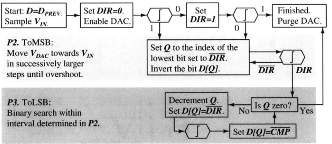
Conventional charge-redistribution SAR ADCs use a capacitive digital-to-analog con-verter (DAC) to generate test voltages which are fed into a comparator along with the input voltage VIN [45]. The conventional SAR logic uses the binary search algorithm to update the approximation of VIN based on the comparator output. The LSB-first SAR ADC presented here also uses a comparator and a capacitive DAC with one minor modification allowing the DAC to output either the lower or upper bound of its input code. This modification is detailed in Section 2.4.
Samp. 1: 9 bitcycles Samp.2: 4 bitcycles Samp.3: 2 bitcycles
Samp.1 Conversion Table Initial guess off by -21 Initial guess off by +2 Perfect initial guess
Bitcycle D[9:0 CMP .864 VIN P1{ 1,2 11010 00110 Lo '--- --- -2 3 11010 00111 Lo P2 4 11010 01111 Lo 848 -5 11010 11111 Hi . -11010 10111 Lo jc P3 7 11010 11011 Hi 8 11010 11001 Lo y832 9 11010 11010 Lo -End 11010 11011 - 0 D[4:0J 6 17 115 131123 127 125 126 1 27 1261241 25
Bit DIR 0 3 4 3 2 1 0 IR O 1 0 DIR
under test
Phase f P1 P2 P3 P1 P2 P3 P1
Initial guess is the value of the prior sample
Figure 2-2: Example 10-bit conversions using the LSB-first SA algorithm. Fewer bitcycles are needed when the initial guess is more accurate. The break in the vertical axis indicates that only a small portion of the 10-bit fullscale range is shown. Only
D[4 : 0] are shown in the timing diagram because D[9 : 51 are never altered by the
algorithm in this example. The bolded binary digits in the table indicate the current bit under test.
LSB-first SA starts with an initial guess D of the current sample's value and bitcycles the least-significant bits (LSBs) of D first instead of the most-significant bits (MSBs) as in conventional SA. Because this ADC is targeted at signals with low mean activity, an initial guess equal to the value of the previous sample DPREV is
effective since the error will be Acode. On average, the algorithm uses a number of bitcycles/sample that scales logarithmically with the error between the guess code and the final output code. Since each bitcycle involves a DAC transition, an analog comparison, and logic transitions, LSB-first SA saves energy in all components of the ADC by performing an N-bit conversion in fewer than N bitcycles/sample when the signal activity lessens.
2.2.1
Algorithm Description
Figure 2-2 depicts the DAC voltage VDAC during three example 10-bit conversions using LSB-first SA and Figure 2-3 contains a flowchart of the algorithm. LSB-first SA has three phases, denoted as P1, P2, and P3. In P1, the INIT phase, the algorithm seeks to determine the error direction of the initial guess and store it in the 1-bit
P1. INIT: Determine error direction of initial guess.
Start: D=Dchr Set DIR= . _lSet Finished.
Sample VIN. Enable DAC. DIR=1 Purge DAC.
1 o0
P2. TMSB:Set Q to the index of the
Move V isc towards VIN lowest bit set o DIRi.
in successively larger Invert the bit D[Q] iIR
DIR
steps until overshoot.
P3. ToLSB: Decrement Q. +-Is Q zero'.
Binary search within Set D[Q]=DIR. No Yes
intervA. determined in P2.
Set D)[Q]=CMP
Figure 2-3: Flowchart illustrating LSB-first successive approximation. The
copara-tor outputs when VDAC >
VIN-register DIR. VIN is sampled and D, the 10-bit input code to the DAC, is set to the Inthiguess of DpEt. DIR is initialized to 0. DIR controls an extra LSB capacitor in the DAC so that when DIR is 0, the DAC output voltage VDAC is set to D's lower bound. When DIR is 1, VDAC is set to D's upper bound.
VDAC is then compared against VIN. If the comparator output CAIP is 1, meaning
VDA4C is greater thani IN, then the initial guess was too high so DIR is kept at 0 denoting the need to decrease the gruess. Inversely, if CMIP is 0 then DIR is set to
1. Inl this case, the initial guess of DpREV1 is either too low or exactly correct. To dlist inguish between these two possibilities, VIN is simply compared to VDAC'. again, since VDAC is now set to the upper bound of DPREV- This process is illustrated in Figure 2-4. The INIT phase takes 1 to 2 bitcycles to complete. When the initial guess is exactly correct, conversion ends after only 2 bitcycles. The first example conversion of Figure 2-2 has all initial guess DPREV = 838 and a, final output code Dotu = 859.
For this conversion DIR = 1 because VDAC is smlaller thall VIN during both bitcycles
of P1.
In P2, the ToMSB phase, the algorithm moves D ill the direction of DIR to converge to the final output code Dou'p. Each bitcycle takes successively larger steps. This is done by setting bits in D to the value of DIR from LSB to MSB until VD4C