Publisher’s version / Version de l'éditeur:
Vous avez des questions? Nous pouvons vous aider. Pour communiquer directement avec un auteur, consultez la première page de la revue dans laquelle son article a été publié afin de trouver ses coordonnées. Si vous n’arrivez pas à les repérer, communiquez avec nous à PublicationsArchive-ArchivesPublications@nrc-cnrc.gc.ca.
Questions? Contact the NRC Publications Archive team at
PublicationsArchive-ArchivesPublications@nrc-cnrc.gc.ca. If you wish to email the authors directly, please see the first page of the publication for their contact information.
https://publications-cnrc.canada.ca/fra/droits
L’accès à ce site Web et l’utilisation de son contenu sont assujettis aux conditions présentées dans le site LISEZ CES CONDITIONS ATTENTIVEMENT AVANT D’UTILISER CE SITE WEB.
ECS Journal of Solid State Science and Technology, 7, 8, pp. R115-R119,
2018-07-28
READ THESE TERMS AND CONDITIONS CAREFULLY BEFORE USING THIS WEBSITE. https://nrc-publications.canada.ca/eng/copyright
NRC Publications Archive Record / Notice des Archives des publications du CNRC :
https://nrc-publications.canada.ca/eng/view/object/?id=58225a6c-31fc-4342-a728-1a0d702c34f4
https://publications-cnrc.canada.ca/fra/voir/objet/?id=58225a6c-31fc-4342-a728-1a0d702c34f4
Archives des publications du CNRC
This publication could be one of several versions: author’s original, accepted manuscript or the publisher’s version. / La version de cette publication peut être l’une des suivantes : la version prépublication de l’auteur, la version acceptée du manuscrit ou la version de l’éditeur.
For the publisher’s version, please access the DOI link below./ Pour consulter la version de l’éditeur, utilisez le lien DOI ci-dessous.
https://doi.org/10.1149/2.0231808jss
Access and use of this website and the material on it are subject to the Terms and Conditions set forth at
Direct-gap photoluminescence from a Si-Ge multilayer super unit cell
grown on Si
₀.₄ Ge₀.₆
Direct-Gap Photoluminescence from a Si-Ge Multilayer Super Unit
Cell Grown on Si
0.4Ge
0.6D. J. Lockwood, 1,∗,zN. L. Rowell,1L. Favre,2A. Ronda,2and I. Berbezier2
1Measurement Science and Standards, National Research Council, Ottawa, Ontario K1A 0R6, Canada
2CNRS, Institut Mat´eriaux Micro´electronique Nanosciences de Provence, AMU, Avenue Normandie Niemen, 13397
Marseille Cedex 20, France
Both Si and Ge possess indirect band gaps, which makes them very inefficient light emitters. One way to overcome this limitation is through bandgap engineering. M. d’Avezac et al. predicted in 2012 that a strained SiGe2Si2Ge2SiGensuper unit cell on Si0.4Ge0.6
would have a direct and dipole-allowed gap of 0.863 eV, which is suited for optical fiber applications. Here we report on the epitaxial growth of such a structure and its optical properties, for which purpose two similar samples were prepared by molecular beam epitaxy and solid phase epitaxy. Photoluminescence (PL) spectra were obtained at low temperatures (6–25 K) with excitation at wavelengths of 405 and 458 nm, which emphasize the light emission from the sample superstructure. A strong low-energy PL quadruplet is seen, with peaks near 727, 758, 792 and 822 meV at 6 K, together with a much weaker peak at 871 meV. The ratio of intensities of the strong and weak peaks is the same in both samples. The weak peak at 871 meV is assigned to the dipole-allowed direct-gap transition associated with the super unit cell. The four strong peaks are attributed to dislocation related emission lines of the thick relaxed Si0.4Ge0.6transition layer.
© The Author(s) 2018. Published by ECS. This is an open access article distributed under the terms of the Creative Commons Attribution Non-Commercial No Derivatives 4.0 License (CC BY-NC-ND,http://creativecommons.org/licenses/by-nc-nd/4.0/), which permits non-commercial reuse, distribution, and reproduction in any medium, provided the original work is not changed in any way and is properly cited. For permission for commercial reuse, please email:oa@electrochem.org. [DOI:10.1149/2.0231808jss]
Manuscript submitted May 18, 2018; revised manuscript received July 16, 2018. Published July 28, 2018. This was Paper 1568 presented at the Orlando, Florida, Meeting of the Society, May 11–15, 2014.
Light emission from Si nanostructures has been of great interest for some time now1owing to the need for silicon-based light sources for applications in silicon photonics.2 Both Si and Ge possess indi-rect band gaps, which makes them very inefficient light emitters.1 Band gap engineering employing quantum wells or quantum dots has been proposed as one way to overcome this limitation.1,3–5Based on this principle Si/Ge and Si/SiGe-alloy thin-multilayer nanostructures grown on Si have been produced.6,7 Although light emission with greatly improved efficiency has been obtained at low temperatures the emission at room temperature is still very weak, because of exciton dissociation.2,7,8Recently, as the result of novel bandgap engineering calculations, entirely new Si/Ge9and Si10structures possessing direct gaps have been proposed. The former structure is based on construct-ing a new super unit cell comprised of multiple epitaxial layers of Si and Ge grown on (001) Si1-xGexwith x ≥ 0.69while the latter structure
comprises a metastable cubic Si20phase with a quasi-direct bandgap
of 1.55 eV.10 According to the energy band diagram calculated by d’Avezac et al.,9 a SiGe
2Si2Ge2SiGen superstructure on Si0.4Ge0.6
should have a direct and dipole-allowed gap of 0.863 eV (1.44 µm), which is ideally suited for photonic data applications since it lies within the common optical-fiber transmission range of 1.3–1.55 µm. Here we report on the growth of such structures and their optical properties.
Experimental
The required Si/Ge layers were grown by molecular beam epitaxy (MBE) on a fully relaxed Si0.4xGe0.6substrate provided by
STMicro-electronics. Before introduction into the UHV growth chamber, the substrates were cleaned ex-situ using a standard chemical process; acid oxidation followed by oxide etching and –H surface passiva-tion. At the conclusion of the chemical cleaning, the samples were immediately transferred into the UHV growth chamber. They were given an in-situ anneal at 750◦
C for 15min and then at 1000◦
C for 15min. A Si0.4Ge0.630 nm-thick clean buffer layer was systematically
deposited at 750◦
C after the anneal. Silicon was evaporated from an electron beam gun and Ge from an effusion cell. Growth rates of both elements were about 1 nm/min with a thickness control at
∗ Electrochemical Society Fellow. zE-mail:david.lockwood@nrc-cnrc.gc.ca
the sub-Angstrom precision level. Measurements of surface topogra-phy and mean root square roughness were carried out with a PSIA XE-100 atomic force microscope (AFM) in air in the non-contact tap-ping mode. Transmission electron microscopy (TEM) cross-section observations were performed using a JEOL2010F with a 200 KV acceleration voltage. Cross-section TEM samples, which were pre-pared by mechanical thinning followed by precision Ar ion polishing, confirmed that the layers were planar and that their interfaces were chemically abrupt.
Two similar samples were prepared by quite different growth meth-ods: MBE and solid phase epitaxy (SPE). In both samples the super-structure (terminated with n = 12 monolayers of Ge) was grown on a 5 µm thick relaxed buffer layer of Si0.4Ge0.6 on a 750 µm thick
(001) Si substrate. The MBE sample was grown conventionally with a 30-nm thick buffer layer of Si0.4Ge0.6 and the superstructure
lay-ers deposited at 500◦C. For the SPE sample, the thin buffer layer
was deposited at 750◦C, but the superstructure layers were deposited
at room temperature (i.e., they were amorphous) and then annealed (i.e., crystallized) at 500◦C for 30 min to reduce the interdiffusion of
Si/Ge at the interfaces. Atomic force microscopy measurements over an area of 15 × 15 µm2showed that the RMS surface roughness was
small at 2.07 and 0.46 nm for the MBE and SPE samples (see Fig.1), respectively, confirming the smoother interfaces in the SPE sample.
The photoluminescence (PL) spectra were measured using a Bomem DA3 FTIR spectrometer equipped with a cooled Ge Ap-plied Detector Corporation detector, with the samples excited at low temperatures with either 70 mW of 405 nm loosely-focused light from a GaN-based semiconductor laser or 35 mW of 458 nm light from an argon ion laser.
Results
As-measured and instrument-response corrected PL spectra ob-tained at low temperature with excitation at 405 nm are shown in Fig.2for the MBE and SPE samples. The relatively sharp lines at 1092 and 1144 meV arise from the Si substrate (transverse optic phonon replica of the Si no-phonon line) and an instrumental emis-sion line, respectively. For this excitation wavelength, the PL from the substrate is weak because the penetration depth of the laser light is relatively small (∼100 nm in Si and ∼20 nm in the Si0.4Ge0.6buffer
16 14 12 10 8 6 4 2 0 2500 2000 1500 1000 500 0 Topography [nm] N u m b er of event s 3.5 3 2.5 2 1.5 1 0.5 0 350 300 250 200 150 100 50 0 Topography [nm] N u m b er of event s
Figure 1. Top panels give AFM images of the MBE sample (left image) and SPE sample (right image). Each full image size is 5 × 5 µm2. The height scale has
been normalized at 20 nm. Bottom panels give the two-dimensional roughness measurements on the full scale images from which the root-mean-square roughness (RMSR) is calculated: MBE sample (left panel) RMSR = 2.07 nm and SPE sample (right panel) RMSR = 0.46 nm. The inset shows a TEM cross-section image of the Si-Ge stacking layers in the SPE sample.
800 1000 1200 1400 1600 1800 0 200 400 600 800 Corrected Raw
Photoluminesecnce intensity (arb. units)
Energy (meV) (a) Raw Corrected MBE x20 6 K 405 nm 800 1000 1200 1400 1600 1800 0 200 400 600 800 1000 1200 Corrected Raw
Photoluminescence intensity (arb. units)
Energy (meV) Raw Corrected (b) SPE x20 6 K 405 nm
Figure 2. As-measured (raw) PL spectra obtained with 405 nm excitation from the (a) MBE and (b) SPE samples at 6 K. Also shown are the PL results for these
700 750 800 850 900 950 0 200 400 600 800 1000 1200 1400
Photoluminescence intensity (arb. units)
Energy (meV) (a) MBE SPE 6 K 405 nm excitation Supercell PL
SiGe buffer layer PL
x20 700 750 800 850 900 950 0 400 800 1200 1600 2000 2400
Photoluminescnce intensity (arb. units)
Energy (meV) (b) MBE SPE 6 K 458 nm excitation x20
Figure 3. Comparison of PL spectra obtained from the MBE and SPE samples at 6 K using (a) 405 and (b) 458 nm excitation.
are emission features from an instrumental source that are not re-moved by the correction for the instrumental response. However, the small dip in the raw spectra evident at 895 meV is mostly removed by the correction process. The sharp drop in response at low energy near 700 meV is due to the cutoff in the instrumental response, and here the instrumental response correction has a considerable effect on the appearance of the spectra; two intense peaks are now seen at ∼730 and ∼760 meV with little change evident in the ∼820 meV shoulder region. Thus no PL was detected from the two samples at low temperature in the energy range 1000–1850 meV, and no PL was seen at room temperature either. From now on we only show results obtained at the lower energies employing instrument corrected spectra.
The PL spectra from the MBE and SPE samples contained similar features, a characteristic that was seen for both 405 and 458 nm exci-tation, as shown in Figs.3and4. This result indicates we are probing the same physical effects, despite the quite different growth condi-tions between the samples. There are, however, significant differences between the samples in overall PL intensity. The PL signal from the SPE sample is more intense than that from the MBE sample, which can be attributed to a higher PL efficiency arising from the sharper
700 750 800 850 900 950 0 500 1000 1500 2000 2500 405 nm 458 nm x2 458 nm 405 nm 405 nm
Photoluminescence intensity (arb. units)
Energy (meV) SPE 6 K 405 nm 458 nm x2 x40 x20
Figure 4. Comparison of the PL spectra obtained with excitation at 405 and
458 nm for the SPE sample at 6 K.
interfaces created in the growth of the SPE sample, and the relative peak intensities for each sample vary slightly depending on the exci-tation conditions (see, for example, the results obtained for the SPE sample shown in Fig.4). In these spectra a strong low-energy PL quadruplet is seen, with peaks near 728, 758, 792 and 822 meV at 6 K, together with a much weaker peak at 871 MeV. The ratio of intensities of the four strong peaks to that of the weak peak is the same in both samples. As can be seen in Fig.5, the intensities of all PL peaks decrease overall with increasing temperature up to 25 K (the fact that the 6 and 20 K spectra are slightly weaker than the 10 and 25 K spectra could be due in part to variations in the sample illumi-nation conditions at the different temperatures; see below for further discussion on this point), but the strong peaks decrease in intensity faster at first than that of the weak peak up to 20 K. However, the situation is reversed by 25 K. At 25 K, the intensities of the strong PL peaks are about half that at 10 K, and exhibit a significant variation in relative intensity with increasing temperature. For example the peak at 822 meV is much lower in intensity at 20 K than it was at 6 K compared with the peak at 728 meV. Because of this, the window to higher energy is enlarged, and at 20 K the weak peak at 871 meV is no longer a shoulder feature and is more clearly visible with respect to the PL noise level than at 6 K (see Fig.5for details).
700 750 800 850 900 950 0 200 400 600 800 1000 1200 1400 20 K 25 K 6 K 10 K
Photoluminescence intensity (arb. units)
Energy (meV) 6 K 10 K 25 K 20 K SPE 405 nm
Figure 5. Temperature dependence of the PL spectrum obtained from the SPE
700 750 800 850 900 950 0 500 1000 1500 2000
Photoluminescence intensity (arb. units)
Energy (meV) (a) SPE 6 K 850 860 870 880 890 900 0 20 40 60 80
Photoluminescence intensity (arb. units)
Energy (meV) (b) SPE 6 K SiGe layer Supercell Fitted spectrum
Figure 6. (a) Curve resolved PL spectrum of the SPE sample at 6 K obtained with 458 nm excitation. (b) Curve-resolving results obtained at higher energy in the
vicinity of the 871 meV PL peak. The solid line shows the fit to the PL data, while component lines are shown beneath the fitted spectrum.
Discussion
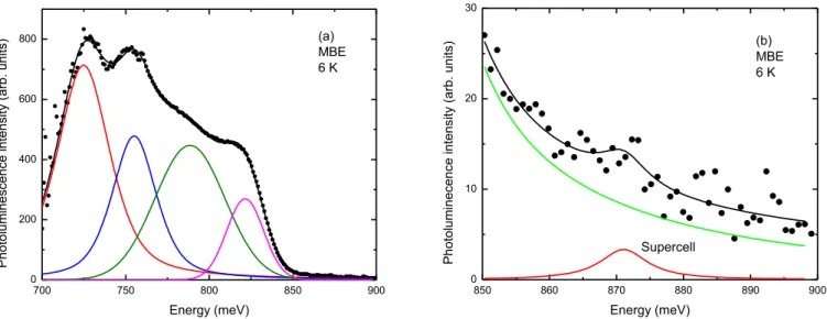
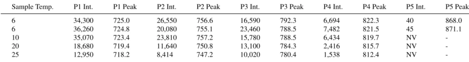
To obtain more detailed information about the structure of the strong peaks and the location of the weak peak, the spectra were curve resolved using a combined Gaussian-Lorentzian lineshape.11 Representative results, as obtained from the raw PL emitted by the SPE sample at 6 K, are shown in Fig.6. Four strong peaks are seen at 728.9, 758.1, 791.8, and 823.1 meV (see Fig.6a) and a much weaker but sharper peak at 871.4 meV (see Fig.6b). A fit to the raw PL results obtained from the same sample at 20 K yielded almost the same energy values of 724.2, 756.5, 781.6, and 812.6 meV for strong peaks and 869.1 meV for the weak peak. Similar results were obtained from fits to PL obtained from the MBE sample, as can be seen in Fig.7.
Given the close agreement in energy, the weak peak at 871 meV ap-pears to be the expected dipole-allowed direct-gap transition predicted to be at 0.863 eV in the superstructure. This peak can be anticipated to be quite weak in PL owing to the fact that this composite layered structure in our samples is only one ‘unit cell’ thick. Apart from the uncertainty in the experimental value arising from the standard error in the fits (∼4 meV), the apparent small difference in energy between theory and experiment could easily be the result of a difference in
strain within the layer in the sample compared with the ideal modeled structure or arise from assumptions made for parameter values in the model. It would be good to be able to verify this assignment by other optical methods such as absorption and derivative spectroscopy that can be used in some cases for bandgap characterization. The direct absorption method is excluded by the thick Si substrate. In the case of derivative spectroscopy, the supercell system here is so thin as to preclude this method. The PL method is sensitive to the bandgap as the emission obtained with this method occurs characteristically at a structure’s bandgap. In fact PL has some definite advantages in this regard for Group IV materials as the excitons created in the rela-tively thick optical penetration region diffuse and congregate in lower bandgap regions, an example of which is the supercell volume. In such systems these exciton diffusion phenomena greatly increase the emission that would otherwise be obtained via direct excitation from such thin, lower bandgap regions.
Because of their high intensity, the peaks near 729, 758, 792 and 823 meV must arise from the Si0.4Ge0.6relaxed buffer layer, which
is the thickest component of the structure apart from the Si substrate itself that contributes only very weakly to the PL (see above). The
700 750 800 850 900 0 200 400 600 800
Photoluminescence intensity (arb. units)
Energy (meV) (a) MBE 6 K 850 860 870 880 890 900 0 10 20 30
Photoluminecence intensity (arb. units)
Energy (meV)
(b) MBE 6 K
Supercell
Figure 7. (a) Curve resolved PL spectrum (here, the spectral data have been smoothed using a four point smoothing procedure) of the MBE sample at 6 K obtained
with 458 nm excitation. (b) Curve-resolving results obtained at higher energy in the vicinity of the 871 meV PL peak. The solid line shows the fit to the PL data, while component lines are shown beneath the fitted spectrum.
Table I. Integrated intensities (in arbitrary units) and peak positions (in meV) of the five component peaks (P1. . . P5) found by curve-resolving the four-point smoothed PL spectrum obtained from the SPE sample at low temperatures (in K). Laser excitation at 405 nm was used at all temperatures, except for the second measurement at 6 K where excitation at 458 nm was used. At 25 K, the PL peak P5 was not visible (NV).
Sample Temp. P1 Int. P1 Peak P2 Int. P2 Peak P3 Int. P3 Peak P4 Int. P4 Peak P5 Int. P5 Peak 6 64,690 728.0 36,480 758.5 23,970 792.4 10,530 822.3 291 871.0 6 116,800 728.5 61,520 757.5 54,610 792.3 18,470 822.9 258 870.2 10 80,630 727.8 36,590 757.6 28,720 790.5 9,130 820.4 93 867.8 20 22,500 721.2 16,310 752.1 14,650 784.7 3,802 814.1 29 869.9 25 41,890 723.7 17,630 754.1 14,080 782.5 2,385 810.7 NV
-Table II. Integrated intensities (in arbitrary units) and peak positions (in meV) of the five component peaks (P1. . . P5) found by curve-resolving the four-point smoothed PL spectrum obtained from the MBE sample at low temperatures (in K). Laser excitation at 405 nm was used at all temperatures, except for the second measurement at 6 K where excitation at 458 nm was used. At 20 and 25 K, the PL peak P5 was not visible (NV).
Sample Temp. P1 Int. P1 Peak P2 Int. P2 Peak P3 Int. P3 Peak P4 Int. P4 Peak P5 Int. P5 Peak 6 34,300 725.0 26,550 756.6 16,590 792.3 6,694 822.3 40 868.0 6 36,260 724.8 20,080 755.1 23,460 788.5 7,482 821.5 45 871.1 10 35,070 723.4 23,810 757.2 15,780 788.5 6,434 819.7 NV -20 18,680 719.4 11,640 750.8 13,100 784.3 2,416 815.7 NV -25 12,950 718.2 8,414 747.2 10,020 780.4 1,538 812.4 NV
-energies of the peaks, however, are much lower than that expected for a bulk Si0.4Ge0.6alloy where the indirect energy gap is 971 meV.7
The energy separations (∼30 meV, as seen from TablesI and II), and general appearance of these peaks is reminiscent of PL that has been attributed to the presence of various dislocation defects (i.e., the four so-called D lines) in Si13–16and SiGe alloys.17,18The observed stronger PL features are in the right energy range for dislocations, if one extrapolates their possible line positions from those of silicon. For example, see the “D1” and “D2” lines discussed by Sauer et al. for silicon.13There is little published work regarding the PL of disloca-tions in SiGe, although we note there is a broadening of the dislocation lines with increasing Ge fraction along with a shift to lower energy as observed by ourselves for a wide range of Ge fractions17and by others for relatively low Ge concentration SiGe samples.18These PL features are quite sharp in Si,13,14but are much broader in higher Ge concentration alloys.17 Further, the variation in their relative inten-sities with temperature together with the large overall changes seen with the change in excitation wavelength for the SPE sample at 6 K, but not so much for the MBE sample (see TablesIandIIand Fig.4), indicates that their source is not intrinsic to the supercell and would be consistent with variations in dislocation densities across the Si0.4Ge0.6
substrate. In that regard, it should be noted that the sample holder used in the experiment held a number of samples and each sample had to be repositioned for runs at different temperatures. In addition, dislocations were observed in transmission electron microscopy in-vestigations of the relaxed Si0.4Ge0.6 substrate on Si. Therefore we
conclude that this strong PL arises predominantly from dislocations formed during the growth of the relaxed alloy substrate layer on the Si wafer.
Conclusions
In conclusion, we have obtained experimental evidence of the pre-dicted direct-gap optically-allowed transition in a special super unit cell comprised of a number of ultrathin layers of Si and Ge. A peak is observed at 871 meV in the PL obtained from two differently prepared samples that is very close in energy to the theoretically predicted di-rect gap of 863 meV for this particular structure. Unfortunately, from a room temperature device point of view, the peak is only observable at low temperatures (<25 K) at this stage. In future work, a major
improvement in the optical efficiency would be obtained by eliminat-ing the dislocations in the Si0.4Ge0.6alloy substrate. The PL intensity
could also be enhanced by growing samples with multiple (e.g., 20) super unit cells, which would provide a greater active volume for direct gap emission.
Acknowledgment
We thank Adrien Gouy´e for the TEM measurements. ORCID
D. J. Lockwood https://orcid.org/0000-0002-3001-2630 References
1. D. J. Lockwood, Ed., Light Emission in Silicon, Academic Press, San Diego (1998). 2. L. Pavesi and D. J. Lockwood, Eds., Silicon Photonics, Springer, Berlin (2004). 3. L. Esaki and R. Tsu, IBM Research Note, RC-2418 (1969).
4. U. Gnutzmann and K. Clausecker,Appl. Phys., 3, 9 (1974).
5. S. A. Jackson and R. People,Mat. Res. Soc. Symp. Proc., 56, 365 (1986). 6. E. Kasper and F. Sch¨affler, in Strained-Layer Superlattices: Materials Science and
Technology, T. P. Pearsall, Ed., pp. 223, Academic Press, Boston (1991). 7. G. Abstreiter, in Light Emission in Silicon, D. J. Lockwood, Ed., pp. 37, Academic
Press, San Diego (1998).
8. D. J. Lockwood and L. Tsybeskov,IEEE J. Sel. Top. Quantum Electronics, 20, 8200807 (2014).
9. M. d’Avezac, J.-W. Luo, T. Chanier, and A. Zunger,Phys. Rev. Lett., 108, 027401 (2012).
10. H. J. Xiang, B. Huang, E. Kan, S.-H. Wei, and X. G. Gong,Phys. Rev. Lett., 110, 118702 (2013).
11. D. J. Lockwood and Z. R. Wasilewski,Phys. Rev. B, 70, 155202 (2004). 12. J. Weber and M. I. Alonso,Phys. Rev. B, 40, 5683 (1989).
13. R. Sauer, J. Weber, J. Stolz, E. R. Weber, K.-H. Kfisters, and H. Alexander,Appl. Phys. A, 36, 1 (1985).
14. W. M. Duncan, P.-H. Chang, B.-Y. Mao, and C.-E. Chen,Appl. Phys. Lett., 51, 773 (1987).
15. G. Davies,Phys. Reports, 176, 83 (1989).
16. S. Fukatsu, Y. Mera, M. Inoue, K. Maeda, H. Akiyama, and H. Sakaki,Appl. Phys. Lett., 68, 1889 (1996).
17. N. L. Rowell, J.-M. Baribeau, and D. C. Houghton, in Proceedings of the
Sec-ond International Symposium on Silicon Molecular Beam Epitaxy;, J. C. Bean and L. J. Schowalter, Eds., pp. 48, Electrochem. Soc. Proc., 88(8), (1988).
18. E. A. Steinman, V. I. Vdovin, T. G. Yugova, V. S. Avrutin, and N. F. Izyumskaya,