HAL Id: hal-03004243
https://hal.archives-ouvertes.fr/hal-03004243
Submitted on 13 Nov 2020
HAL is a multi-disciplinary open access
archive for the deposit and dissemination of
sci-entific research documents, whether they are
pub-lished or not. The documents may come from
teaching and research institutions in France or
abroad, or from public or private research centers.
L’archive ouverte pluridisciplinaire HAL, est
destinée au dépôt et à la diffusion de documents
scientifiques de niveau recherche, publiés ou non,
émanant des établissements d’enseignement et de
recherche français ou étrangers, des laboratoires
publics ou privés.
Electric Field and Current Conduction Modelling in
Bi-layers Insulations HVDC Aeronautic Cables
E Diaw, Séverine Le Roy, G. Teyssedre, E Aubert
To cite this version:
E Diaw, Séverine Le Roy, G. Teyssedre, E Aubert. Electric Field and Current Conduction Modelling in
Bi-layers Insulations HVDC Aeronautic Cables. IEEE Internat. Conf. on Dielectrics (ICD), Valencia,
Spain, 5-9 July 2020., Jul 2020, Valencia, Spain. pp. 505-508. �hal-03004243�
Electric Field and Current Conduction Modelling in
Bi-layers Insulations HVDC Aeronautic Cables
E. N. Diaw, S. Le Roy, G. Teyssèdre
LAPLACE, Université Paul Sabatier CNRS, INPT, UPS
Toulouse, France
E. Aubert
Technical and Innovation Department, Safran Electrical Power Blagnac, France
Abstract- For decades, electrical energy network in aircrafts
was based on relatively low voltage (mainly 115V ac and 28V dc), providing the power to the different energy functions of the aircraft. Great strides have been made in the new aircraft generations, notably the A380 and the Boeing 787, with an increase of the aircraft size, and with the input of electrical energy in replacement of certain hydraulic or pneumatic actuations. Today, there is a tendency to replace HVAC network with HVDC (+/-270 V dc, 540 V dc and higher in the future) network in order to benefit from these many advantages. This increase of the electrical energy pushes the transmission cables to their limits and leads to questions about the impact of these new constraints on the aeronautic cables insulation. This article presents a macroscopic model and comparison between simulation results and measurements made on bi-layer materials used in actual aeronautic cable insulation. The electric field distribution within materials and kinetic of interfacial charges build-up are analyzed.
Keywords—HVDC aeronautic cables; cables insulations; current measurement; macroscopic models, field inversion, interfacial charge.
I. INTRODUCTION
Electrical energy occupies a minority place since the beginning of the history of aeronautics and until recently compared with the mechanical, pneumatic and hydraulic energies, which are mainly run. With the increase of the size of planes and the related needs in embedded power, aeronautic electrical networks experience permanent progress and today, electrical energy takes a more and more important part, to the detriment of other energies vectors with new architectures [1,2]. This transition to the more electric aircraft is not without consequences and thus requires the control of new technologies to meet the requirements of the high electrical power.
Studies show that, in energy transmission in terrestrial HVDC networks [3], cables insulation materials can accumulate space charge, and macroscopic models are used to predict electric field distribution [4,5]. In fact, with HVDC systems, electric field is driven by electrical conductivity, which is usually dependent on temperature and electric field, even for materials used in aeronautic domain [6-8]. In the perspective of more electric aircraft, insulating materials behaviour has been investigated by performing experimental
characterization on two materials used as insulation in aeronautic cables: Polytetrafluoroethylene and Polyimide (PTFE) and Kapton FN [9]. Measurements have also been performed on bilayer materials PTFE/PI, to achieve a more realistic characterization. Macroscopic modelling based on electrical conductivity function of temperature and electric field was used to predict the electric field distribution considering different geometries.
II. EXPERIMENTAL METHODS AND MACROSCOPIC MODEL
A. Current measurements
PTFE and PI (polyimide, Kapton FN) film samples used for current measurements are metallized on both sides with 50 nm-thick gold layer of 20 mm diameter. Kapton FN samples have a thickness ranging from 30 up to 36 μm. Kapton FN contains a FEP layer (fluorinated ethylene propylene) on each face. PTFE films are 72 to 77 µm-thick.
Current measurements results were obtained on bi-layer samples (PI/PTFE) at 50°C for electric fields ranging from 1 to 120 kV/mm for 3 hours of polarization and 3 hours of depolarization. These experimental data will be used to validate simulation results on bi-layer samples for different geometries.
B. Macroscopic models
In the literature, macroscopic models are proposed to determine electric field distribution in cables [4,5]. Modelling is performed using COMSOL Multiphysics® software. Model resolution is performed using the three equations below
(1)
(2)
(3)
Here J is the current density, Je an external current density, ρ is the net charge density, V is the applied voltage and E is the electric field. The main input of this model is the electrical conductivity, which varies upon temperature and electric field.
Current measurements have already been performed on Kapton and PTFE samples separately [9] to deduce an electrical conductivity law as a function of field and temperature for each material [9-10]. This conductivity is of the form, for both materials:
(4) where T is the temperature in °C and E the electric field in
V/m. A, C, T0, E0 and α, are constants, presented in Table 1
for Kapton and PTFE respectively. Permittivity is considered as constant for both materials (3.4 for Kapton and 2.1 for PTFE).
Two types of simulations have been performed:
- A plane parallel sandwich geometry: a PTFE of thickness 76.2µm is set on top of a Kapton sample of thickness 31µm. The voltage is applied on the Kapton, while the PTFE is grounded. The simulation is in one dimension, the origin (y=0) is set on the Kapton side. For these simulations, the temperature is supposed constant. The simulation results are given at steady-state.
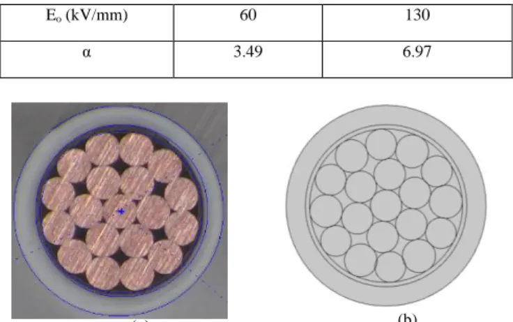
- A cable geometry inspired by a DR16 cable (Fig. 1). DR16 cable consists in a 1.45 mm diameter conductor. PI insulation is 41 µm thick and PTFE insulation is 185 µm thick. This model represents the real geometry of DR16 cable, taking account the cylindrical bi-layer insulation and the metal strands. Voltage is applied on the metal strands. We suppose that the outer layer of the cable is grounded. Real characteristics of air gaps like the nature of gas, its electrical conductivity and dependencies are not modelled. The model is resolved in non-isotherm conditions, the power being injected in the conductor. Temperature modelling is based on the time dependent heat transfer equation, of the form:
(5)
where Cp is the heat capacity at constant pressure, ρp is the
material density, k is the thermal conductivity and Q is the heat generated from the conductor by Joule effect, which is:
(6)
where I is the current in the conductor, ρcu is the
temperature-dependent resistivity of copper and A is the cross section area of the conductor. The boundary condition is set to be convective heat flux at the outer layer of the cable with ambient air temperature of 20°C.
TABLE 1: PARAMETERS FOR ELECTRICAL CONDUCTIVITY LAW. Parameters PI PTFE A (S/m) 2.3×10⁻¹⁶ 4.5×10⁻¹⁶ To (°C) 80.5 106.7 C (°C-1) 0.04 0.04 Eo (kV/mm) 60 130 α 3.49 6.97 (a) (b)
Fig. 1. DR16 cable (a) and cylindrical geometry cable model (b)
III. RESULTS
A. Model Results on plane-parallel Bi-layer sample
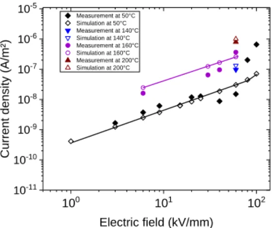
Fig. 2 shows a comparison between experimental current densities and simulated ones on a plane-parallel sandwich of Kapton/PTFE, for mean applied electric fields ranging from 1 to 120 kV/mm at 50°C and 160°C. Comparisons are also proposed for a single mean electric field (60 kV/mm) at different temperatures (140 and 200°C). At 50°C and for electric fields below 60 kV/mm, simulated current density is close to the measured one. Beyond 60 kV/mm, the model and measurements diverge. At this temperature, this difference may be because the bi-layer model does not really represent the real system, as the bilayer behavior of Kapton film is not detailed. It is also possible that for relatively high fields, the variation in electrical conductivity alone is not sufficient to predict the behaviour of the bi-layer insolation, and that other physical mechanisms come into play. For the other experimental data (different electric fields at 160°C and different temperatures at an electric field of 60 kV/mm), the simulated results are close to the experimental ones.
With the macroscopic model, it is possible to obtain the electric field distribution across the Kapton/PTFE sandwich, which is more difficult to obtain experimentally. Fig. 3 presents the electric field distribution across the sandwich for different mean applied fields at 50°C. For mean electric fields below 60 kV/mm, the electric field is higher in the Kapton compared to PTFE. The electric field distribution in each material is not only dependent of the permittivity variation. The electrical conductivity value has a dominant impact. Previous current
Fig. 2. Experimental results on current density vs electric field in bilayer with 3h charging time compared to steady state current from model.
Fig. 3. Electric field distribution in a PI/PTFE bi-layer model calculated at 50°C. Legend shows average electric fields
measurements on one material alone show that at 50°C, PTFE is less conductive than Kapton for electric fields below 60 kV/mm, and becomes more conductive above that field. The inversion of higher electric field from Kapton to PTFE is directly linked to this variation in relative value of electrical conductivity.
The electric field inversion is also observed when the temperature increases. Fig. 4 shows the simulation results for a mean applied field of 40 kV/mm for temperatures of 50 and 90°C. As previously, this inversion is explained by the fact that beyond a certain temperature value, PI becomes more conductive than PTFE.
Current transient can also be compared to simulation results. Fig. 6 shows an example of measured and simulated current transient for a mean field of 60 kV/mm, at 50°C. A nearly constant current is observed in the simulation as opposed to the measured current density. This different behavior may be explained by the fact that the conductivity equation has been developed considering that after 3 hours of polarization; the current achieved the steady state. From what is observed in Fig. 5, this is clearly not the case, and experimentally, other processes not linked to conduction (polarization as an example) certainly play a non-negligible role. The simulated results are relatively correct when the time considered in long (above 1000s).
Fig. 4. Electric field inversion on bi-layer model. Average field of 40 kV/mm
Fig. 5. Experimental and simulated transient current density in bilayer at mean field of 60 kV/mm at 50°C
Between two materials of different conductivity and permittivity, an interfacial charge builds up, and can be quantified by Maxwell-Wagner’s theory. The following equation defines the interface charge for a PI/PTFE bi-layer:
(7)
with (8)
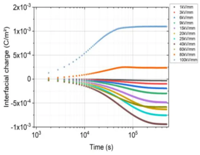
The sign of the interfacial charge and its dependence in time depends on the variation of the electrical conductivity of the two materials which is driven by electric field and temperature. Fig. 6 present the calculated interfacial charge as a function of time for different mean electric fields at 50°C. For electric fields below 80 kV/mm, the interfacial charge is
negative. A steady state is reached for times above 1.105 s for
applied fields below 80 kV/mm, well above the experimental 3hours of voltage application. The larger the field applied, the faster the charge stabilizes. For fields ranging from 1 to 40 kV/mm, the steady state interfacial charge increase. After 40 kV/mm, the interfacial charge decreases and becomes positive for fields above 80 kV/mm.
100 101 102 10-11 10-10 10-9 10-8 10-7 10-6 10-5 Measurement at 50°C Simulation at 50°C Measurement at 140°C Simulation at 140°C Measurement at 160°C Simulation at 160°C Measurement at 200°C Simulation at 200°C Curr en t d en si ty (A/m² ) Electric field (kV/mm) PTFE PI PTFE PI
Fig. 6. Time-dependent interfacial charge for a PI/PTFE bi-layer model at 50°C
B. Model Results on a bi-layer cable geometry
Simulations have been performed for a bi-layer cable geometry, on the basis of DR 16 real aeronautic cable. In this configuration, the electric field within the cable radius is non-homogenous. Moreover, local electric field intensification takes place in air gaps at the interface between metal strands and Kapton. This also has an impact on the electric field inside the Kapton and PTFE insulations. Fig. 7 presents the electric field distribution within the cable calculated for an applied voltage of 1 kV on the conductor with a current intensity of 15 A, which corresponds to an average field of 3.88 kV/mm and a temperature of 40°C on the conductor.
Electric field within PI is closed to 10 kV/mm. This value is higher than the applied field on the conductor and can be explained by the fact that, at the contact with a metal strand, a local electric field intensification affects the one found in Kapton insulation. Within PTFE, calculated electric field is close to 2.8 kV/mm and is lower than the one in Kapton. In all cases, the calculated electric field in each material is lower than the material dielectric breakdown.
Fig. 7. Electric field map on DR16 cable model
It is to note that the electric field calculated in the air gaps is relatively high compared to the breakdown field in air, as no attempt has been made to simulate the conductivity variation in air with temperature and electric field. The actual simulated results in Kapton and PTFE are certainly overestimated. It will be important in the future to be able to take into account the true nature of the gas between the metal strands and the
variation in its electrical conductivity as a function of electric field, temperature and pressure.
No experimental measurements are available on DR16 cables to compare the simulated current values issued from the macroscopic model to experimental ones. Experimental current measurements were performed on a DR8 cable (same as DR16 with 3.85 mm diameter conductor. PI insulation is 50 µm thick PI and PTFE insulation is 200 µm thick) for temperatures ranging from 30°C to 90°C with mean electric fields from 1 kV/mm to 20 kV/mm. Fig. 8 shows a comparison between experimental current densities and simulated ones on DR8 model cable at 50°C. AT this temperature and field range, a good correlation is observed between simulation and measurements also on cable
geometry. However, it will be interesting to perform current
measurements on DR8 cable for fields higher than 20 kV/mm as the threshold in field is clearly above this value for both materials.
Fig. 8. Comparison between measurements and simulation on DR8 cable
IV. CONCLUSIONS
A macroscopic model is proposed to predict the electric field distribution in plane parallel bi-layer Kapton/PTFE samples and in real aeronautic cable geometry with multilayers insulation. Depending on the applied voltage on the conductor, or on the temperature value, the maximal electric field can be localized either in the PI layer or in the PTFE layer. This behavior is directly linked to the interfacial charge, that can be positive or negative depending on the experimental conditions (voltage and temperature). In real cables, the same behavior takes place, i.e. an inversion on the maximal electric field from Kapton to PTFE with temperature and/ or filed. Care will be taken in the future in the modelling of air gaps, that has been observed as having a non negligible impact on the electric field distribution inside both insulations.
REFERENCES
[1] V. Madonna, P. Giangrande, and M. Galea, “Electrical power generation in aircraft: Review, challenges, and opportunities,” IEEE Trans. Transp.
Electrific., vol. 4, pp. 646-659, 2018.
[2] B. Sarlioglu and C. T. Morris, “More electric aircraft: Review, challenges, and opportunities for commercial transport aircraft,” IEEE
[3] G. C. Montanari, “The electrical degradation threshold of polyethylene investigated by space charge and conduction current measurements,”
IEEE Trans. Dielectr. Electr. Insul., vol. 7, no. 3, pp. 309-315, 2000.
[4] P.H.F. Morshuis, R. Bodega, D. Fabiani, G.C. Montanari, L.A. Dissado and J.J Smit, “Calculation and measurement of space charge in MV size extruded cables systems under load conditions”, IEEE Int. Conf. Solid
Dielectr., Winchester (England), vol. 2, pp. 502-505, 2007
[5] M. Jeroense and P. Morshuis, “Electric fields in HVDC paper-insulated cables”, IEEE Trans. Dielectr. Electr. Insul., vol. 5, pp. 225-236, 1998. [6] E. Motyl and R. Kacprzyk, “On the electrical conduction in polyimide,”
IEEE Int. Symp. Electrets (ISE), Shanghai (China), August 1996, pp.
608-613.
[7] M. A. Sussi and G. R. G. Raju, “Electrical conduction currents in polytetrafluoroethylene,” IEEE Int. Conf. Electr. Insul. Dielectr. Pheno.
(CEIDP), Pocono Manor (USA), pp. 313-318, 1990.
[8] J. U. Lee, C. H. Kim, S. Lee, J. B. Wang, D. Kim, and S. S. Lee, “Non-linear conduction properties of polytetrafluoroethylene film,” IEEE Int.
Symp. Electr. Insul., pp. 149-152, 1992
[9] E. N. Diaw, S. Le Roy, G. Teyssedre, and E. Aubert. “Current measurements on insulating materials used in aeronautic HVDC cables,”
Proc. MEA (More Electrical Aircraft) Conference, Toulouse, 2019.
[10] E. N. Diaw, S. Le Roy, G. Teyssedre, and E. Aubert. “Current Measurements in High Performance Polymers used in Aeronautic Cables,” submitted.