Dynamic Modeling, Simulation, and Control of a
Series Resonant Converter with Clamped
Capacitor Voltage
by
Terrence Tian-Jian Ho
B.E., Electrical Engineering, The Cooper Union (1992)
Submitted to the Department of Electrical Engineering and
Computer Science
in partial fulfillment of the requirements for the degree of
Master of Science in Electrical Engineering
at the
MASSACHUSETTS INSTITUTE OF TECHNOLOGY
January 1994
©
Terrence Tian-Jian Ho, MCMXCIV. All rights reserved.
The author hereby grants to MIT permission to reproduce and
distribute publicly paper and electronic copies of this thesis
document in whole or in part, and to grant others the right to do so.
Author
...
Department of Electrical Engineering and Computer Science
January 14, 1994
Certified
by...
...
George C. Verghese
Professor of Electrical Engineering
/\-
n
f\.
Thesis Supervisor
Accepted by
...
Frederic Morgenthaler
Chairman, Departmental Committee on Graduate Students
i
I
OA.
Dynamic Modeling, Simulation, and Control of a Series
Resonant Converter with Clamped Capacitor Voltage
by
Terrence Tian-Jian Ho
Submitted to the Department of Electrical Engineering and Computer Science on January 14, 1994, in partial fulfillment of the
requirements for the degree of Master of Science in Electrical Engineering
Abstract
A modified series resonant converter with clamped tank capacitor voltage exhibits complex dynamic characteristics due to the clamping diodes. This thesis aims to understand the dynamic behavior of the converter in a three-dimensional state-space. Geometric features of the state trajectories are analyzed and sampled-data models are developed. Based on the small-signal model around nominal operation, a feedback controller is designed. Nonlinear control rules are established to deal with large deviations from the nominal. The study is supported by simulation results obtained using a specially constructed simulator.
Thesis Supervisor: George C. Verghese Title: Professor of Electrical Engineering
Acknowledgments
First and foremost, I wish to express my deepest gratitude to my thesis advisor, Professor George Verghese. He gave me guidance when I needed direction. He gave me ideas when I was lost. He gave me encouragement when I was about to give up. His knowledge, his patience, and his energy have helped to make the arduous process of completing a thesis a bit less trying and a bit more pleasant for me. His advice went beyond the mere technical issues. His friendship I enjoy and appreciate tremendously. For all these, I am grateful.
I would like to thank Mr. Chiharu Osawa who started the project. His initial research was extremely valuable in laying the ground work upon which my research was built. He gave me his precious time to introduce me to the project, all during the busiest hours of his final preparation of his own thesis and return to Japan.
I would like to thank Dr. Boris Jacobson at Raytheon who partially funded my research. Our discussions provided much insight.
I would like to thank the National Science Foundation for its generous financial support. It is my honor and good fortune to receive the NSF Graduate Fellowship.
I would like to thank all members of LEES for providing a friendly working envi-ronment.
I sincerely thank my friends for being their great selves. Their diligence, their optimism, their confidence, and their energy have not only impressed me but also motivated and transformed me. They have shown me, by example, the limitless possibilities of human achievements. From them, I have learned to live a fuller, better, more balanced, and more care-free life. I feel truly fortunate to be in company of such capable a group of people.
I am forever indebted to my parents whose genuine love and unwavering support are seldom professed through words but always quietly delivered through actions. My debt to them is one that cannot be repaid in a lifetime. If any of my meager accomplishments can bring them some joy, then I shall dedicate this thesis to them.
To My Parents, Whose Love and Support Will See Me Through It All
Contents
1 Introduction 13
1.1 Background ... 13
1.2 Objectives ... 15
1.3 Thesis Organization ... 15
2 SRC Circuit Operations and Simplifications 17 2.1 A Brief Overview of Series Resonant Circuits ... 17
2.2 Modeling Simplifications of the SRC with Clamped Capacitor Voltage 20 3 Topological Modes and State-Space Models 24 3.1 Topological Modes ... 24
3.2 Boundary Conditions and Their Representation in 3-D State-Space . 25 3.3 State-Space Equations ... 28
3.4 Symmetry Among Topological Modes . ... 28
4 Velocity Fields of State-Space Trajectories 34 4.1 Topological Mode MO . . . ... 34
4.2 Topological Modes M5 and M6 ... 37
4.3 Topological Modes M7 and M8 . ... 39
4.4 Topological Modes M1, M2, M3, and M4 . ... 39
5 Trajectory Geometry 44 5.1 Topological Modes M1, M2, M3, and M4 . ... 44
5.1.2 Trajectory Geometry in M2, M3 and M4 . ... 48
5.1.3 Discontinuous Conduction Mode S3 . ... 48
5.2 Topological Mode MO ... 50
5.3 Topological Modes M5, M6, M7, and M8 ... 52
5.4 A Summary ... 52
6 Steady-State Characteristics 54 6.1 Average Output Current ... 54
6.2 Operating Modes ... 55
6.3 The Selection of a Nominal Operating Point ... 59
7 Analytical Models 63 7.1 Large-Signal Sampled-Data Model . . ... 63
7.1.1 Formulation ... 64
7.1.2 Application to SRC at the Selected Nominal Point ... 65
7.1.3 Simulation and Analytical Computation Results ... 68
7.2 Small-Signal Sampled-Data Model ... . 70
7.2.1 Formulation ... 70
7.2.2 Application to SRC at the Selected Nominal Point ... 72
7.2.3 Simulation and Analytical Computation Results ... 73
8 Controller Design 76 8.1 Transfer Function of the Plant ... 76
8.1.1 Approximate Converter Transfer Function ... ... . 77
8.1.2 Output Stage and Load Requirements . ... 79
8.1.3 Approximate Plant Transfer Function . ... 81
8.2 Small-Signal Feedback Controller and Performance Evaluation ... . 82
8.3 Nonlinear Control Rules and Performance Evaluation ... 89
8.4 Disturbance Feedforward and Performance Evaluation ... 93
8.5 Initial Start-Up Behavior ... 96
9.1 Simulator Structure ... 101
9.2 Core Simulation Programs ... . . 102
9.2.1 SRC Transient Response, srctrans.m ... .. 102
9.2.2 Evaluation of State at the Next Time Point, nextval.m .... 105
9.2.3 Determination of Topological Modes, ckcfg.m ... 106
9.2.4 Switching Signals, eswitch.m ... 107
9.2.5 Locating Exact Switching Times, edtexact.m ... 107
9.3 Auxiliary Functions .... ... 108
9.3.1 Average Output Current, iavg.m ... 108
9.3.2 Output Display, plsrc.m ... 109
9.3.3 3-D Animation, anim.m. .... ... . 110
9.3.4 Feedback Controller, fbctrl.m . . . . .. .... 110
9.3.5 Other Auxiliary Functions . . . ... . 110
9.4 Simulation Calling Programs .... ... . . . 112
9.4.1 Trajectory Fields, simO.m, siml.m, sim5.m, sim7.m .... 112
9.4.2 Searching for the Nominal Phase Angle, simnom.m ... 112
9.4.3 Steady-State Operating Modes and Average Output Current, simsss.m, simsssi.m simssa.m, simssm.m . . . . 113
9.4.4 Nominal States at Switching Times, simsyo.m ... 113
9.4.5 Small-Signal Transition Matrices, simsyq.m ... . 114
9.4.6 System with Feedback Controller, simplt.m, simctr.m simstr.m 114 10 Conclusion 116 A Simulator Source Codes 118 A.1 Core Programs .. ... 118
A.2 Auxiliary Programs . ... 127
A.3 Simulation Calling Programs .... ... ... 135
A.4 Other Programs ... 155
B.1 Source Codes and Results in Maple ... 157 B.2 Simulation Results from simsyq.m ... 161
List of Figures
2-1 A simple series resonant circuit: (a) basic topology, and (b) magnitude
of the admittance Y(jw) with L = 2/H, C = 0.2/LF, and R = 2Q. .. 18 2-2 Full bridge SRC (from [3]) ... 20 2-3 Schematic diagram of the SRC with clamped tank capacitor voltage,
with C = 0.2/tF, L1 = L2 = 1H, RL = 0.0181i, CL = 10,OOOF,
E = 200 to 350V, n = 8, and f = 275kHz ... 21
2-4 Waveforms of the switches and equivalent voltage sources. ... 22 2-5 Simplified circuit diagram ... 23 3-1 A three-dimensional representation of the topological modes of the SRC. 27 4-1 Velocity fields in mode MO for (a) el = E and e2 = 0, (b) el = 0 and
e2= E, (c) el = 0 and e2 = 0, (d) el = E and e2= E ... 36
4-2 Velocity fields in mode M5 for (a) e1 = E and e2 = 0, (b) el = 0 and
e2 = E, (c) e = 0 and e2= 0, (d) el = E and e2=E ... 38
4-3 Velocity fields in mode M7 for (a) e1 = E and e2 = 0, (b) el = 0 and
e2 = E, (c) e = 0 and e2= 0, (d) el = E and e2 = E ... 40
4-4 Velocity fields in mode M1 for (a) el = E and e2 = 0, (b) e = 0 and e2= E at various levels of vc and with E = 200V ... 42
4-5 Velocity fields in mode M1 for (a) el = 0 and e2 = 0, (b) e = E and
e2= E at various levels of vc and with E = 200V ... 43
5-1 A sample trajectory in Ml with el = e2 = E = 250V, vp = nVL =
5-2 A sample trajectory in M3 with el = OV, e2= E = 250V, vp = nVL =
8 8.5V, i(0) = 90A, i2(0) = 40A, vc(O) = -60V ... 49
5-3 3-D trajectory from zero initial state under nominal operating conditions. 53 6-1 Average output current characteristics for various supply voltage levels with nVL = 8 -8.5V. ... 55
6-2 Operating modes for nVL = 8 8.5V. . . . ... 57
6-3 Time responses from zero initial state at nominal operating point of = 115.625°, E = 250V, and nVL = 8 8.5V . ... 60
6-4 Projections of state variables at nominal operating point of b = 115.625°, E = 250V, and nVL = 8 8.5V. ... 61
8-1 Three different models for the output stage: (a) constant voltage source, (b) capacitor in parallel with resistor, and (c) capacitor in parallel with current source. ... 79
8-2 Bode plots of the plant transfer function ... 81
8-3 System with small-signal feedback controller. . . . .... 82
8-4 Bode plots of transfer functions K(s), T(s), S(s), and C(s)... 84
8-5 Output voltage, nvL, (a) without feeback and (b) with feedback, and feedback signal Ab ... 86
8-6 Output voltage, nvL, and feedback signal, AqO, for system starting with il(0) = 0,i2(0) = 0,vc(0) = 0 ...
87
8-7 Output voltage, nvL, and feedback signal, AO, with initial AnvL = -1V. 88 8-8 Output voltage, nvL, and feedback signal, AO, (a) from full-load to no-load with only linear feedback (b) from full-no-load to no-no-load to full-no-load with nonlinear control ... 91
8-9 Output voltage, nvL, and feedback signal, AO!, from initial nvL = 50V (a) with a resistor output model and (b) with a current source model. 92 8-10 Output voltage, nvL, and feedback signal, AqO, with supply voltage, E, droops from Eno ,,= 250V at -V/cycle (a) without disturbance feedforward, and (b) with disturbance feedforward. ... 94
8-11 System block diagram. ...
8-12 Output voltage, nvL, and feedback signal, AO$, from start-up with con-stant supply voltage, E, at 250V (a) with resistor output model, and (b) with current source output model. ...
8-13 Output voltage, nvL, and feedback signal, A, from start-up with drooping supply voltage, E, from 300V at -V/switching cycle (a) with resistor output model, and (b) with current source output model. C-1 Trajectory in operating mode 0 from zero initial state at = 40°,
E = 150V, and nVL = 8 8.5V . ...
C-2 Trajectory in operating mode 1 from zero initial state at = 70°,
E = 250V, and nVL = 8 8.5V.
C-3 Trajectory in operating mode 2 from zero initial state
E = 200V, and nVL = 8 -8.5V . ...
C-4 Trajectory in operating mode 4 from zero initial state
E = 280V, and nVL = 8 -8.5V . ...
C-5 Trajectory in operating mode 5 from zero initial state
E = 350V, and nVL = 8 8.5V . ...
C-6 Trajectory in operating mode 6 from zero initial state
E = 180V, and nVL = 8 -8.5V . ...
C-7 Trajectory in operating mode 7 from zero initial state
E = 325V, and nVL = 8 8.5V . ...
C-8 Trajectory in operating mode 8 from zero initial state
E = 275V, and nVL = 8 8.5V . ...
C-9 Trajectory in operating mode 9 from zero initial state
E = 250V, and nVL = 8.8.5V . ... at 5 = 120°, at . . at at 0. . .
at q
. . at b at qb at ; . . . . . = 120°, = 110°, . . . . . = 150°, = 1300°, = 160°, = 180°, 95 98 99 164 . . . .165 166 167 168 169 170 171 172List of Tables
3.1 Boundary conditions for the topological modes. ... 26
3.2 Matrices for state-space representation of the SRC. ... 29
3.3 Symmetric regions among topological modes ... 31
3.4 Symmetric regions within topological modes ... 32
5.1 State transition matrices in continuous conduction mode ... 51
Chapter 1
Introduction
1.1 Background
There are many variations in the design of resonant converters, but most designs share the same operating principles. The switches in the resonant converter generate a square wave (+E and -E) or a quasi-square wave (+E, 0, and -E) from a dc voltage source (E). This voltage waveform is applied across a resonant LC circuit tuned to approximately the switching frequency to filter out the unwanted harmonics. Output power may be controlled by adjusting the switching frequency, since the gain drops off as the switching frequency moves away from the resonant frequency. If a quasi-square wave is used as the input to the LC circuit, power can also be controlled by adjusting the duty ratio of the quasi-square wave. One common application of resonant converters is in high-frequency dc/dc power supplies. The ac current through the LC circuit is rectified and low-pass filtered to produce dc. An isolation transformer may precede the rectification.
One advantage of resonant converters is lower switching losses at high switching frequency as compared to other types of dc/dc converters, since the switching can be done when the current or the voltage is nearly zero. The higher operating frequency reduces the size of energy storage components in the power converter and thus the size of the converter itself. The disadvantage, on the other hand, is that the on-state
A related disadvantage of the resonant converter is the high peak capacitor voltage in series resonant converters or the high peak inductor current in parallel resonant converters. In the series case, with increasing LC circuit filter selectivity as measured by the quality factor, Q, the peak capacitor voltage can be Q times the source voltage.
A similar situation exists for the inductor current in the parallel case.
To combat this undesirable feature, the series resonant converter (SRC) under investigation in this project has four clamping diodes placed around the resonant tank capacitor to ensure that the voltage across the resonant tank capacitor can never exceed the input voltage. The inductor and the primary side transformer are split into two sections. This converter was developed at Raytheon by Jacobson and DiPerna, [2]. The introduction of the clamping diodes was intended to improve the performance of the converter under heavy load conditions. However, it resulted in a large variety of possible operating modes, some of which may not be desirable in normal operation of the converter. On the other hand, it also presented us with the challenge of understanding the complex dynamics of the SRC and thereby developing better feedback control.
Earlier numerical simulations of the steady-state behavior of the SRC based on circuit models were carried out by Raytheon [2] and by Kato and Verghese [4, 5]. They had demonstrated the complexity of the boundaries between operating modes of the circuit. Simulations based on state-space models and aimed at analyzing the dynamic behavior of the SRC were done by Osawa in his Master's thesis [7]. His simulation results in general agreed with what Raytheon and Kato had done, but a few discrepancies in the region of discontinuous conduction mode, for example, remained. The behavior of the state-space trajectories was analyzed. It was shown that only four of the nine diode conduction configurations, or topological modes, need to be analyzed. The others can be derived from these four because of symmetries in the state-space models. Of the nine possible topological modes, one was analyzed in detail in [7].
1.2 Objectives
The chief goal of this thesis is to obtain a more complete understanding of the dynamic and steady-state behavior of the SRC in the face of the added complexity of operating modes due to the clamping diodes. The analysis of the state-space trajectories is to be aided with a computer simulation program, specially tailored for this circuit in order to achieve a high degree of accuracy, speed, and flexibility.
The properties of the SRC around the nominal operating point are to be examined through derivation and analysis of sampled-data models. A feedback controller will be designed utilizing classical control methods. The goal here is to deliver constant output power to the load and to maintain steady output voltage in the presence of slow fluctuations in supply voltage, or other such disturbances, and modeling uncertainties.
1.3 Thesis Organization
We will start with a brief overview of resonant converter circuits and an introduction to the basic operation of the series resonant converter in Chapter 2. We will also discuss the justification for some simplifications in the circuit model of our SRC.
In Chapter 3, the different topological modes of the SRC, their boundary con-ditions, and their state-space equations are stated. Also shown are some symmetry properties that may simplify circuit analysis.
In Chapter 4, the trajectories are analyzed through their velocity fields, which provide some simple but limited understanding, especially when the motion is confined to a plane. The velocity fields are less helpful for more complicated motions, due to difficulty in visualization.
Trajectory geometry is further analyzed in Chapter 5. Because of the simple structure of the state-space equations, closed-form equations of the trajectories can be easily derived. Descriptions of the trajectories in the various modes are presented.
Steady-state operating characteristics are described in Chapter 6. The selection of a nominal operating point focuses the small-signal analysis to one specific condition.
Analytical models - large-signal and small-signal sampled-data models in partic-ular - are derived and analyzed in Chapter 7. The results are obtained with the aid of the symbolic computation capabilities of Maple, and verified by simulation.
A controller design is presented in Chapter 8. Simulation results of the closed-loop system under various operating conditions are examined.
Chapter 9 gives a description of the structure and the design of the simulation program, which is written in Matlab. Key features and a guide to the simulation programs are outlined.
Chapter 2
SRC Circuit Operations and
Simplifications
2.1 A Brief Overview of Series Resonant Circuits
It is worthwhile to take a look at a simple series resonant converter (SRC) first, to have some basic idea of how it works. A more complete and detailed treatment on this topic can be found in Chapter 9 of [3].
Figure 2-1(a) shows the basic topology of the series resonant converter. The admittance of the series RLC circuit seen by the source is
1 sC 1 2as
(s
+ R)
s
2LC
+ sRC +
1 R(s
2+2as + )
where wo = /1/C is the resonant frequency and 2a = R/L is the width of the
half-power or 3 dB points. The quality factor, Q = wo/2a, is a normalized measure of the filter's selectivity. The higher the value of Q, the sharper the frequency response,
IY(jw)l. The magnitude of the frequency response of a sample Y(jw) with L = 2H, C = 0.2ptF, and R = 20, is shown in Figure 2-1(b). The quality factor for this set of
parameters is
i
v
a VcCR
(a) 104 105 106 107 108 (b) Figure 2-1: A simple series resonant circuit: (a) basic topology, and (b) magnitude of the admittance Y(jw) with L = 2H, C = 0.2.uF, and R = 2.At resonance, s = jwo, the admittance Y(jw) is 1/R. The load voltage across the
resistor is equal to the source voltage. The capacitor voltage, however, is Q times the source at the resonant frequency. The transfer function from va to vc is
Vc(s) _ 1 1 -W2 -Y(s (2.3) Va(s)
sC
s2LC + s RC + 1
(2+ 2as
+ w)(2.3) At resonance, where w = wo Vc | ao Q (2.4) Va 2aEven for a modest Q, the peak capacitor voltage, or the peak inductor current in the parallel resonant converter case, can be excessively high. This is one major disadvantage of resonant converters. The series resonant converter under study in this thesis uses diodes to clamp the capacitor so that the peak capacitor voltage is limited to within + the source voltage. This, however, makes the dynamic behavior
of the circuit more complicated, as we will see in later chapters.
When the input voltage is a square wave with an operating frequency close to w0,
and if Q is relatively large, the filtering of the harmonics by the LC circuit is effective. Since the magnitude of Y(jw) drops as we move away from the resonant frequency, output power can be controlled by adjusting the switching frequency. This technique presents two disadvantages. How far the switching frequency can be varied is limited by switch limitations or the presence of the third harmonic. If the Q of the circuit is not very high, the range of control is limited since a relatively large change in the switching frequency is necessary to achieve a relatively small change in output power. An alternative approach to frequency modulation for output power control is phase modulation. A quasi-square wave, instead of a square wave, constitutes the source across the resonant circuit. This can be achieved by placing the RLC circuit inside a full bridge, as shown in Figure 2-2. The SRC analyzed in this thesis is a variation of this bridge topology, as we shall see later. Power control is achieved by varying the duration (2 a) for which the input voltage is 'clamped' at zero volts, since the the magnitude of the fundamental of the quasi-square wave is 4E cos a. The corresponding 'duty ratio' of the applied voltage is /r = 1 - (2a/7r). One added
E E -E-I
a
n-a
o
I I S2 Sl,4 S1,4 S1,3 I SFigure 2-2: Full bridge SRC (from [3]).
advantage of phase modulation control, as suggested in [10], is that it allows the design of filters and magnetic components to be optimized at a specific frequency, which improves the efficiency of these components.
2.2 Modeling Simplifications of the SRC with
Clamped Capacitor Voltage
In conventional dc/dc series resonant converters, the output ac current is rectified and filtered. An isolation transformer is often used to couple the load with the LC circuit. The modified SRC designed by Raytheon differs from the conventional SRC in two ways. One is the clamping diodes around the tank capacitor, and the other is
I
D5 io
Figure 2-3: Schematic diagram of the SRC with clamped tank capacitor voltage, with C = 0.21 F, L1 = L2 = 1lH, RL = 0.0181Q2, CL = 10, 0001LF, E = 200 to 350V,
n = 8, and f, = 275kHz.
the splitting of the inductor. Figure 2-3 shows the schematic diagram of the modified circuit with its nominal component values. The diodes and switches are assumed ideal throughout our development. If S1, S2 and S3, S4 are switched in the complementary
manner shown in Figure 2-4, we may represent the voltage applied to the resonant circuit via voltage sources el and e2, which are both square waves (0, +E) of the same
frequency, but with a phase difference. This is shown in Figure 2-5. The voltage across the resonant circuit is el - e2.
For state-space descriptions, it is natural to take capacitor voltages and inductor currents as state variables. The conventional SRC can be modeled with two state variables as there is only one capacitor and one inductor. Its state-space trajectory can be easily represented in 2-D. The circuit in Figure 2-3, however, will then be a fourth-order system. This poses a problem for graphical representation and visualization. Some reasonable approximations can be made, however, so as to reduce the order of the system. The output capacitor CL in our case is 10, 000F, which is quite large. The output filtering is therefore highly effective, and the voltage across the load does not fluctuate much during typical operating conditions, so we may treat the load as a constant voltage source, as shown in Figure 2-5. Given that a constant output power
S1 S2 S3 S4 I I I
-I
e2 I I E-T/2-Figure 2-4: Waveforms of the switches and equivalent voltage sources.
of 4kW is to be maintained, the equivalent voltage source, VL, is therefore roughly 8.5 volts. With this approximation, the circuit in Figure 2-5 is third-order.
We will model the output stage of the converter as a constant voltage source in most of our analysis of the converter. In the actual SRC circuit built by Raytheon, the output current is hard to measure because of physical constraints, so for the feedback controller, only the output voltage can be measured. Obviously, the constant voltage approximation is then no longer adequate. We will at that stage model the output either as a load resistor in parallel with the capacitor, as in Figure 2-3, or as a constant current source in parallel with the load capacitor.
The supply voltage, E, is not constant. It droops slowly, and its rate of change is much lower than that of the state variables. This slow variation in supply voltage will be treated as disturbance in the control design. In the analysis of converter dynamics,
I
D5
V
-L
D6
Figure 2-5: Simplified circuit diagram.
E is assumed to be constant.
The real circuit components also have parasitic capacitances and resistances, which pose various problems, particularly in ensuring well-behaved switching. We will not include any of these parasities in our circuit model. Their omission does not have a large impact on dynamic modeling for purposes of controller design.
We then arrive at the simplified circuit model in Figure 2-5 for the series resonant converter with clamped capacitor voltage. This is the model that we will use in analysis and simulation. Again, the output stage has to be modeled a little differently in control design.
Chapter 3
Topological Modes and
State-Space Models
3.1 Topological Modes
The circuit shown in Figure 2-5 is piecewise LTI: we can write linear, time-invariant state-space equations for each combination of the diode conduction state configura-tions, i.e. for each topological mode. The natural state variables are il(t), i2(t), and
vC(t). For the six diodes in the circuit, there can be no more than 26 = 64 different
combinations of conduction states, but some combinations are not possible. We will consider the clamping diodes on the primary side of the transformer and the output rectifying diodes on the secondary side separately in order to keep the classification more manageable. For the clamping diodes, there are a total of nine topological modes. They are
MO all off
M1 D on M5 Dl on and D4 on M2 D2 on M6 D2 on and D3 on M3 D3 on M7 D1 on and D3 on M4 D4 on M8 D2 on and D4 on
The output current is a transformed version of il(t) + i2(t), rectified by the two
secondary-side diodes. The two diodes also determine the sign of vp(t) when in con-tinuous conduction. Disconcon-tinuous conduction occurs when both output diodes are off and the output current is zero. The three topological modes associated with the output diodes are
3.2 Boundary Conditions and Their
Representa-tion in 3-D State-Space
Diode currents and voltages determine the conduction states of the diodes, which in turn determine the topological modes of the SRC. Diode current is positive and diode voltage is zero when the diode is on, and diode current is zero and diode voltage is negative when it is off. However, it can be shown [7] that the conditions on diode currents and voltages that determine the topological modes may be rewritten in terms of conditions on the three state variables, il(t), i2(t), vc(t), and the input switching
voltages, el(t) and e2(t). Since the values of the state variables and input voltages
are readily available in simulation, this simplifies the determination of topological modes in that diode currents and voltages need not be calculated. The boundary
conditions are listed in Table 3.1. Detailed derivations of these boundary conditions are presented in Chapter 10 of [7].
A three-dimensional representation of the topological mode conditions in the state-space is shown in Figure 3-1. The topological modes that occupy planes ('plane modes') and those that occupy space region ('volume modes') are drawn separately for clarity. As can be seen from Table 3.1, conditions for M1 through M8, and for S1 and S2 involve only the state variables. Mode MO occupies the i = i2 plane with the
additional condition el
$
e2. The reason for this will be explained in Chapter 4, whenwe discuss the trajectory fields in MO. S3 also has an additional contraint involving
S1 D5 on and D6 off S2 D5 off and D6 on S3 both off
Topological Mode Boundary Conditions il = i2 MO -E < vc < E el 5 e2 M1 il > i2
O< vc
E
M2 il < i2 -E < vc O M3 il > i2 -E < vc < O M4 il < i2 O < vc < E M5 il > O,i2 > Ovc = E
M6 il < O, i2 < Ovc = -E
M7 il > 0, i2 < 0 VC = 0 M8 il < O,i2 > 0 VC = 0 S1 il + i2 > 0 S2 il + i2 < 0S3
il + i
2=
el - e2- 2nVL < vc < el - e2 + 2nVLV, /7 of ' A
0-0v
00
iP-·3b~;'the input voltages and the load voltage. The il +i2 = 0 plane, as shown in Figure 3-1, is only a possible region for S3. The actual S3 mode may only lie in a part of that plane.
All the topological modes now hold a one-to-one correspondence between their three-dimensional representation in the state-space and their boundary conditions. Therefore, given a point in the state-space, the corresponding topological mode can be determined immediately from Figure 3-1. (At the boundaries between two modes, the converter can be considered to be in either or both modes.) The conditions specified in Table 3.1 are conditions for sustained operation in each mode, so the trajectory will remain within the particular mode until it reaches the edge and enters a different mode. A change in topological mode as a result of a change in the input voltages occurs only with MO and S3, since only their boundary conditions involve el and e2. The input voltages do influence the directions of the trajectories in all cases, though.
3.3 State-Space Equations
For each of the topological modes of the SRC, the state-space equations can be written in the form
*(t) = Ajx(t) + Bju(t)
(3.1)
where x(t) = [il(t) i2(t) vc(t)]T, Bju(t) is a vector and is a function of ei(t), e2(t),
and vp(t), and j denotes the topological mode. Detailed derivations of these equations are shown in [7]. They are listed in Table 3.2 for reference.
3.4
Symmetry Among Topological Modes
The symmetry in the structure of the SRC suggests possible symmetry in its tra-jectories in the state-space. The similarities among the various state-space matrices listed in Table 3.2 are also an indication. Three types of symmetry were found by Osawa [7]: symmetry about the origin, about the MO plane, and about the line
Continuous Conduction (S1 or S2) Discontinuous Conduction (S3) vp = nVLsign(il + i2) vp = (el - e2- vc)/2 O O T2~L el -e -2vp 2L 0 0 0 0 Ao = o - Bou= o C -,, Ao 0O ,Bou = O
c
0 0
O - 0
C0
O °-0 e -E- 0 v,. L 2L +e2-2E2LA LBjU = -e2+E-vD A- O O 1 ,Blu -e-2+2E
____ L,BlU 0 L 2L , 2L
O C O C O 0
A2 = [O 00 O -_ 0 , = el-VP _ _ A2 = ° ° O O 2B2U = e - 2
L
1°2L
2LA
Bu = B -e2-V A2 B3u - 2-2E0 O Uoo 1[ ° L1 1E-v, '
[
r
L 1]
0 2L ' 2L=l- 2 - 0
AO 5= O ,B5u= -2-V e0
I 0 0 0
A6 0 0 B3U -E-vp
L
, -el el 2E2L00 0 0 0 ICLo O O] L 0 I O 2L V j L | *o o 1 _ |_ ° ° °_ 1 _L cL_ A- el -v 0 el +e2 L
o
2L 2L]
A4 O0 O Bu = -2-p L A = 0 2L B4u = -e22Ll-
0 0
0
C C 0 il = i2 = 0 00 -E-vp 0 elv
= E As ,Bsu - -e2-v el = E 0 0 0 I I 0 e:=0LoO
0LO
'
lO
Table0~~~~~~~~li eS = 0 0 0 0 e I -,~P L 0c 0 0E ,lue:-2 A7 = 0 B Bu -e2+E-o 0 0 A -0 el BpU= +E L 2L L 2LA= 00 0 ,Bsu= -':-P As= 0 0 0 Bsu =
-ei-L0 0L
0 0 0
0
0
il + i2 = O, vc = O. Two trajectories (ila(t), i2a(t), vca(t)) and (ilb(t), i2b(t), vcb(t))
are symmetric about the origin if
(ilb, i2b, VCb) = (-ila, -i2a, -VCa) (3.2)
dilb di2b dvcb _
dt ' dt ' dt
for all t. The trajectories are symmetric
dil. di2a dvca\
dt ' dt '
dt
about the MO plane if
(ilb, i2b, VCb) = (i2a, ila, VCa)
and
(
dilb di2b dCb di2a dila dcdt ' dt ' t
d
t ' dt
'
dt
They are symmetric with respect to the line il + i2 = 0, vc = 0 if
(3.3)
(3.4)
(3.5)
(3.6)
(ilb, i2b, VCb) = (-i2a,-ila,-VCa)
and
dilb di2b db di2a dila dvca (37)
dt ' dt ' dt dt ' dt ' dt
Table 3.3 lists the symmetric regions among different topological modes, with their corresponding combinations of input voltages. The proofs are relatively simple and the one for the M1, M2 pair is illustrated below. The others are stated here without proof. Refer to [7] for more detail.
At a point in Ml, xl,
*1 = Alxl + Blu (3.8)
At the corresponding point in M2, x2 = -x1,
i = -A
2X
1+ B
2u
(3.9)Mode with (ei,e2) w.r.t Mode with (el,e 2) (0, 0) (E, E)
(M,
E)
(E, O)
(E, )
(0, E)
(E,E)
___(0,0)
(O, 0) (E, E)M4 (0,E) origin M3 (E,0)
(E, )
(O,
E)
(E,E)
___(0,0)
(0, 0) (E, E)
M6 (0, E) origin M5 (E, 0)
M6
(E,0)
(E, )
origin
M5
(0,E)
(O,
E)
(E,E) _ _ (0, 0) (O, 0) (E, E) M8 (0,E) origin M7 (E ) (E, 0) (0, E) (E,E) ___ (0, 0) (0, 0) (E, E) M4 (0, E) MO (E,0) (E, 0) plane (0, E) (E, E) (0, 0)
(0,0)
(E,E)
M3 (0, E) MO (E, 0)(E,0)
plane
(0,E)
(E,E)
__ _ _(0,0) (0,0) line (0,0) M3 (0, E) (E,o0)(E,0)
1+i2(0,
E)
(E,E)
V=0
(E,E)
(0,0) line (0,0) M4 (0,E)
(E,0) (E,0) = (0i, E)(E,E)
(E,E)
Mode with (el,e 2) w.r.t Mode with (el, e2) MO (0, E) origin MO (E, 0) (O,E) (E,O) M5 (0, 0) il = i2 M5 (0, 0)
(E,E)
(E,E)
(O,E) (E,O) M6 (0, 0) il = i M6 (0, 0)(E,E)
(E,E)
(O,E) (E,O) M7 (0, 0) il + i2 = 0 M7 (0, 0)(E,E)
(E,E)
(0, E) (E, 0) M7 (0, 0) il + i2 = 0 M7 (0, 0)(E,E)
_(E,E)
Table 3.4: Symmetric regions within topological modes.
For the two points to be symmetric with respect to the origin,
=
*1 -/c2 (3.10)
Since A1 is equal to A2, this means that Blu must be equal to -B 2u. Note that
Blu =
el -E-v I L -e +E-vr L 0 x1 el -vp L -e 2-vP L X2 (3.11)Since x2 = -xl and v = nVLsign(il + i2), it follows that vplx, = - vplx2
.
Thecombinations of el and e2 at xl and x2 that will satisfy (3.11) are
el = 0, e = 0 at xl and el = E, e2 = E at x2
el = 0, e2= E at xl and el = E,
e
2=0
atx
2el = E, e2 = 0 at xl and el = 0, e2 = E at x2
el = E, e2= E at x1 and el = 0, e2= 0 at x2
-Symmetry properties also exist within a topological mode itself. Again, without proof, a list of the symmetric regions is shown in Table 3.4. This type of symmetry is most evident in the velocity fields shown in Chapter 4.
These symmetry properties effectively reduce the analysis of the state-space trajec-tories to only four modes: MO, M1, M5, and M7. The trajectrajec-tories in other modes can be derived from them. The symmetry of the circuit suggests that when the switching is also done symmetrically, the steady-state limit cycle will have two half-cycles that are symmetric with respect to the origin. This will be confirmed in Chapter 6.
Chapter 4
Velocity Fields of State-Space
Trajectories
The velocity vector of the state trajectory at any point in the state-space, for some combination of input voltages and load voltage, can be found directly from the state-space equations in Table 3.2. A graphical representation can be obtained by plotting out the trajectories for a short period of time from a number of different state-space locations. The resulting diagrams, which will be called the trajectory velocity fields, give a clear picture as to where and how fast the trajctories will move at various points in the state-space. The plots shown in this chapter are generated using a value of E = 200V and VL = 8.5V for 0.05lisec.
4.1 Topological Mode MO
Topological mode MO was analyzed in some detail in [7]. None of the clamping diodes is conducting in this mode, so the two inductor currents, i and i2, must be equal.
To stay in MO, ve must satisfy
-(el +
e
2) <
C
<
2E-(el
+
e
2)
When el = e2, v = 0 is the only value that can satisfy both conditions. However,
with a nonzero inductor current, vc cannot be maintained at zero and the above conditions are immediately violated. The trajectory will then leave mode MO. The combination of vc = 0, i = 0, and i2 = 0 is a trivial solution. This situation is
illus-trated in Figure 4-11 where i and i2 are plotted against vc for the four combinations
of input voltages. The trajectories in (c) and (d) for the case of el = e2 start on the
il = i2 plane, but i vs. v and i2 vs. vc do not coincide as time goes on, showing
a difference in i and i2. The trajectories obviously do not stay on the i = i2 plane
except for the starting point. Thus, to sustain operation in MO, the input voltages must be different. MO is, in fact, the only M mode in which a condition involving the input voltages el and e2 is required.
Given that the two input voltages are not the same, topological mode MO repre-sents the i = i2 plane in state-space with vc limited to between +E and -E because
of the clamping diodes. Since the two inductor currents, i and i2, are equal, the
order of the circuit is reduced to two, and a plot of either i vs. vc or i2 vs. VC is
adequate for analysis of the trajectories. Both i vs. vc and i2 vs. vc are plotted
in Figures 4-1(a) and (b), but because the two overlap each other, only one graph is visible. The velocities of the trajectories depend on circuit parameters and the initial locations. It is a simple matter to derive them from the state-space equations listed in Table 3.2.
From Figures 4-1(a) and (b), some general properties of the trajectory in this mode can be seen. When the inductor current is positive, it charges up the capacitor, and vc increases. Negative current reduces the capacitor voltage. If the initial current is large enough, the capacitor voltage will eventually reach +E or -E, at which time the SRC enters M5 or M6, respectively. Figures 4-1(a) and (b) are symmetric with respect to the origin, a property described also in [7]. The mode numbers with parentheses, shown in Figure 4-1 and the velocity fields on the next few pages, are the topological modes the trajectories can move into once they reach the boundaries.
One condition for discontinuous conduction, S3, is i + i2 = 0. On the MO plane,
(a) Trajectories in MO for el=E, e2=0 (M5) 200 \ . o -o0 o. - -( ) -4 150 - % (. (4- o
',
'100
'-~
'(S33
' ' 0 (S 1() (4- (I.- f (6 -50 - af
' -200 - (3 o 0 o o ( ( (7 (M6) -50 0 0 il,i2(c) Trajectories leaving MO for e 1=0, e2=0
200() Trajetories leaving M for el5), e2=
200-o- A A - -150 / A - -"" 100 - y & A K B-'~,- "% 50 -0 -N . ) b) -50
-100
- (
v
\
--150 -.. -- '~ W V V -200 -0 0 0 o (M6) I -50 0 il,i2 50(b) Trajectories in MO for el=O, e2=E
200 150 100 50 0 -50 -100 -150 -200 U -50 0 50 il,i2
(d) Trajectories leaving MO for el=E, e2=E
(M5) 200 -/q/%A""_4 -,.: . :- o 150
-
A A A. -- -,","%, 100 f ') 50 - ( -50 , a - o v )-',
-100 N(b...4
--
\$ -150 , ...---- ''W'
V-200
- o o
c
o o 'V
\/
(M6) -50 0 il,i2 50Figure 4-1: Velocity fields in mode MO for (a) e = E and e2 = O, (b) e = 0 and
e = E, (c) e = 0 and e2 = 0, (d) e = E and e2 = E. U (M5) -) /) /A) .) )H )
-,
, /,)
A)
,-, ,,)
%
(p
pa
0t -)t)-o -- (4 a o -0t) N \o -, (-0-
(o- ( -o ' , )-(M6) i )
S3 can occur only on the vc axis, where il = i2 = 0. The additional condition on vc says that the region for S3 is also limited to E - 2nVL < vc < E for el = E and e2 = 0, and -E < v < -E + 2nVL for el = 0 and e2 = E. With the state-space
matrices Ao and Bou in Table 3.2, it can be shown that the derivatives of all state variables in S3 are zero. Therefore, once the trajectory reaches S3, it will stop moving until input conditions change. This effect is shown on the top part of the vc axis in Figure 4-1(a) and on the bottom part in Figure 4-1(b). Osawa referred to this as the 'wall' on the vc axis, where the trajectory cannot move from one side to the other [7]. On the remaining part of the vc axis where S3 cannot be sustained, the trajectory simply passes through. Osawa called this the 'window.'
4.2
Topological Modes M5 and M6
When the capacitor voltage attempts to increase beyond E, diodes D1 and D4 turn on so that vc is clamped to E. The circuit operation in this mode M5 is relatively simple. As the inductor currents must be positive, the circuit is guaranteed to be in continuous conduction mode S1. The load voltage referred to the primary side,
vp, is positive, so the voltages across the two inductors are negative for all of the
four combinations of input voltages. For any particular set of input voltages, the inductor voltages are constant. As a result, i and i2 decrease linearly at a constant
rate, independent of the values of il or i2, until one or both of them drop to zero.
Depending on which current drops to zero first, D1 or/and D4 turn off and the SRC enters M4, M1, or MO. The rate of change in the inductor current depends only on the input voltage combination and not on the location of the trajectory, as can be seen in Figure 4-22.
Topological mode M6 is the dual of M5. The two are symmetric with respect to the origin. Plots of trajectories in M6 will not be repeated here.
2
(a) Trajectories in M5 for el =E, e2=0
60 ,
50so / / / /' 40 (M4) / / / / / 20 10 -10 M0 (M) 0 20 40 6 ii(b) Trajectories in M5 for el=0, e2=E
0
(c) Trajectories in M5 for el=0, e2=0
60 50 40 30 -(M4) 20 10 (M1) -10 0 20 40 0 20 40 60 ii
(d) Trajectories in M5 for el =E, e2=E
60
il
0 20 40 60
ii
Figure 4-2: Velocity fields in mode M5 for (a) e = E and e2 = 0, (b) e = O0 and
e2 = E, (c) e = 0 and e2 = 0, (d) e = E and e2 = E.
4.3
Topological Modes M7 and M8
In topological mode M7, the two upper diodes D1 and D3 are on, so the capacitor voltage is zero. M7 is entered from either M1 or M3. Transition between M1 and M3 without entering M7 occurs when the two inductor currents are in the same direction. Note that vc changes sign during the transition, but cannot stay at zero. Only when
i1 is positive and i2 is negative do both D1 and D3 turn on. The voltage at both ends
of the tank capacitor is +E now.
Once the combination of input voltages and the sign of vp are known, the voltages across the inductors are constant. The trajectories should then move at a constant rate, independent of the magnitude of the inductor currents. The S3 plane divides the M7 plane into two regions, S1 and S2. Trajectories in S1 and S2 are symmetric with respect to the line il + i2 = 0 for input voltage combinations el = 0, e2 = 0
and el = E, e2 = E. Trajectories for el = E, e2 = 0 in Figure 4-33(a) and those for
el = 0, e2 = E in Figure 4-3(b) are also symmetric. For the values used in simulating
Figure 4-3, E - 2nVL > O. The voltage condition for sustainable S3 operation is not satisfied on the M7 plane for el = E, e2 = 0 and el = 0, e2 = E, so S3 does not exist
at; all in these two cases. One the other hand, for el = 0, e2 = 0 and el = E, e2 = E,
the voltage condition for S3 is satisfied, and S3 is the i + i2 = 0, vc = 0 line on the
M7 plane. As can be seen in Figures 4-3(c) and (d), the trajectories tend towards S3. Once they reach S3, depending on the input voltages, they either move towards the origin or stop moving altogether.
Topological mode M8 is the dual of M7. The two are symmetric with respect to the origin.
4.4
Topological Modes M1, M2, M3, and M4
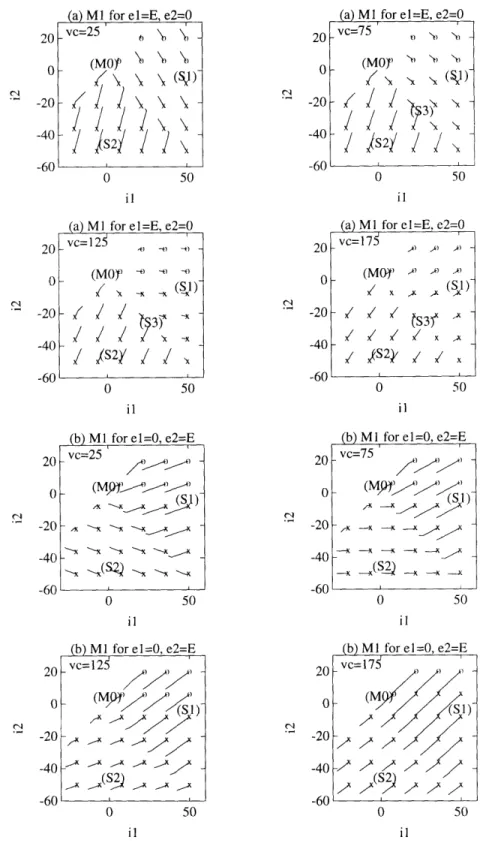
The velocity vectors in volume modes can be derived from the state-space equations as before. Unlike where the trajectories travel on planes, in M1, M2, M3, and M4,
(a) Trajectories in M7 for el =E, e2=0 10 I
0\, (1)\ \ \
-10 0 (M3) , -30 \450 2) \ \
--60 0 20 40 61 ii C" 0(c) Trajectories in M7 for el=0, e2=0
10 M1) 0 -1 - -1\ 1 - '- --20 (M- -30 -40 -50 -60 ' ' ' 0 20 40
(b) Trajectories in M7 for el=0, e2=E
10 (M1) 0 -10 -20 M )
-30
_
-40 -50 -60 0 20 40 6 ii 0(d) Trajectories in M7 for el =E, e2=E
10 (M1) 0 -10 -20 M3) / S/ -50 -60 60 0 20 40 ii 60 il
Figure 4-3: Velocity fields in mode M7 for (a) el = E and e2 = 0, (b) el = 0 and
they move through space. This makes the visualization of the trajectory fields difficult even if 3-D imaging is used. Not only is it difficult to visualize a bunch of short curves in space from their projections, it is equally difficult to see them in a 3-D plot from any one perspective, due to the lack of depth. Fortunately, the vc component of the trajectory velocity vector in modes M1 to M4 is either -d = dt C il or v = i2 (See
dt C
Table 3.2). Therefore, not much information is lost by projecting the trajectory field onto the i vs. i2 plane at various levels of vc.
In M1, the vc component of the trajectory vector is directly proportional to i2. In
Figures 4-44 and 4-5, projections of the trajectories starting at four different values of vc are plotted. For positive i2, the trajectory comes out of the paper towards the
reader in the direction of the vc axis, and for negative i2, it goes into the paper. To
indicate the direction of the vc component, an o is marked at the starting location in the former case, and an x is marked in the latter case. Moving from one value of
vc to the next, we can see the gradual changes in the i and i2 components of the
velocity vectors.
The condition on vc for sustaining S3, stated in Table 3.1, dictates what part of the i + i2 = 0 plane belongs to S3. For the simulations done here, E - 2nVL > 0. S3 is then confined to a band near v = 0, or v = E, or vc = -E, depending on the input voltages. In M1, where vc is positive, when el is equal to e2, S3 occurs in the
lower range of vc around 0 from -2nVL to 2nVL. When el = E, e2 = 0, S3 occurs in
the upper range of vc near E from E - 2nVL to E. For el = 0, e2 = E, S3 does not
exist at all since in this case vc would have to be negative. This is why sometimes in Figures 4-4 and 4-5, S3 is not labeled because it does not exist.
The trajectories in M2, M3, and M4 are related to those in M1 through the symmetry properties stated in Table 3.3. The analysis is similar and thus will not be repeated here.
(a) MI for e1 =E, e2=0 vc=25 , -(MO0 ) \) \,
$ i
S2/ \
0 20 0 -20 -40 -60 50 ii(a) MI for el=E, e2=0
vc= 1 2 ) -4) *)-) (M -x - -I/ I (SI) -/ / /
-x
//S2/
/ / I I 0 2C C -2C -40 -60 50(a) MI for e l =E, e2=0
vc=75 "
'I)
-(MO ""
"%
_/ S2j
3 I 1 I 0 50 il(a) M for e I =E, e2=0
0 50 ii (b) MI for el =0, e2=E 0 il 20 0 -20 -40 -60 50 ii
(b) M1 for el=0, e2=E vc=125
- S(Si)
-'X - -r I, ( I / /5ql
ae
em
0 20 0 -20 -40 -60 50(b) Ml for el=0. e2=E
0 50
iil
(b) MI for el=0, e2=E
0
il
50
il
Figure 4-4: Velocity fields in mode M1 for (a) el = E and e2 = 0, (b) el = 0 and
e = E at various levels of vc and with E = 200V.
20 0 -20 -40 -60 2( c( " -2( -40 -6( vc=175 (M0) 'k) k) ) / x x x (') ) / x S3 ,x1) / x/ / / x x / JS2/ / / x I II I 20 0 -20 -40 -60 vc=25 /x \x (S1) - x x -'-x -- x x -x X --x -x(S2) , -x -_ vc=75 - )K (S1) /-x -- x x x - "x A A -x - -x x ---
* --
-x -x
x(S
2C -2C -4C -6C7777/
7 7(S) ",) \ , . , I \ , . -v -= 1 -7 -I "I', I l) J20 C' -2( -4( -6( 0 2( -2( -40 -60 50 il
(a) M1 for el=0, e2=0 vc=12 O -
\N\ \e\
\x \ X X ( I II O X X R X Xln t--~-c-t
0 50 ii(b) Ml for el=E, e2=E vc=25 ' X / (Si) ," x" x/ x-' x ,3 0 0 50 ii 2 -2
(a) M1 for el=0, e2=0 vc=175
O0
- _.--O.
-0 \n
N(N
-. ,x 20 0 -20 -40 -60 50 0 50 ii(b) MI for e I =E, e2=E vc=75 /3 / / - -- X- S3 / AX- X- A- X- X& 7i 0 50 ii
(b) M1 for el=E, e2=E vc=12 -x\s / / 7/ X\ IS X XS X I
7
0 20 0 -20 -40 -60 50 ii ii(b) M I for e I =E, e2=E vc=17
/ /
/I
()
IN N N
ii
Figure 4-5: Velocity fields in mode M1 for (a) el = 0 and e2 = 0, (b) el = E and
e2 = E at various levels of vc and with E = 200V.
(a) M1 for el=0, e2=0 vc=25
--, i I
o£ -XS
O Ist
(a) M for el=0, e2=0 vc=75 l .t . . 2C -2C -40 -60 20 0 -20 -40 -60 5:l 20 0 -20 -40 -60 I I vv 0 50
Chapter 5
Trajectory Geometry
The trajectory velocity fields give a good picture of the speed and direction of the trajectories at different points in the state-space. However, they are not adequate for topological modes M1 to M4, which occupy space regions, because of difficulty with
3-D representation and visualization.
The trajectories of the conventional series resonant converter in 2-D consist of segments of circular arcs when plotted against normalized axes. Even with the ad-ditional inductor current in our SRC, we may guess that the 3-D trajectories in our case will be arcs on spheres or cylinders when plotted against normalized axes. The trajectory velocity fields in the last chapter have already given some indication of this.
5.1 Topological Modes M1, M2, M3, and M4
In Table 3.2, we listed the state-space equations for each of the topological modes. The differential equations may be solved to obtain closed-form expressions for the trajectories. The relatively sparse state-space matrices suggest relatively simple
solu-tions. Trajectory behaviors in Modes M1, M2, M3, and M4 are similar, as indicated by the symmetry properties. A more detailed analysis of mode M1 in continuous conduction is presented here first. Trajectory behavior in the other modes and in dis-continuous conduction mode S3 can be derived in the same manner, and are briefly
described.
5.1.1
Analysis of Trajectories in Mode M1
The state-space equations for M1 in continuous conduction mode are
dil
el - E - vp
dt L di2-Lv +
C
-e2 + E- P(5.1)
dt L + dvc 1 . dt CInductor current i is completely decoupled from the other two state variables. Its evolution in time is linear. The interaction between i2 and vc can be seen by cross
multiplying the second and the third equations:
1 di2 1 dye -e2 + E - vp dc
2- -- VC
dt +
L(5.2)
C dt L dt L dt
Integrating this, we get
1 2 1 2 -e2 + E - vp
2' + 2' L _ _ = K' (5.3)
where is K' is a constant determined by the initial conditions. This is true for any set of constant values of el, e2, and V,, that is, as long as we remain in the same
switching state and the same output S mode. Rearranging (5.3), we have
('i
2)
+
[ UVC
-(-e
2+E
-vp)]
=K
(5.4)
where K is a constant. This is the equation for an ellipse. The trajectory plotted against normalized axes of %/ i 2vs. x v is an arc of a circle centered at vC (-e2+ E - v) with radius v/K. It is clear that the center is determined by the input
switching voltage, which is just e2 in this case, and the transformer voltage, v,, whose
I UU
0-0 -10-00-0-
-100-
-200-il
Figure 5-1: A sample trajectory in M1 with el = e2 = E = 250V, vp = nVL = 8-8.5V,
i1(O) = 90A, i2(0) = 40A, vc(O) = 60V.
starting position of the trajectory. Since
x/
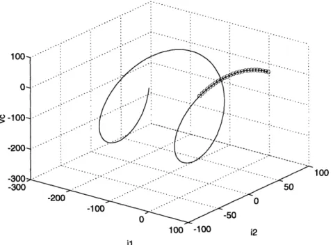
il is a linear function of time, the state-space trajectory is then a spiral on the surface of a cylinder whose axis is parallel to the aL%.il axis and intersects the x/Uvc axis. Figure 5-11 shows an example of the spiraling trajectory in M1 for el = e2 = E = 250V, vp = nVL = 8 8.5V, and the initial conditions i(O) = 90A, i2(0) = 40A, vc(O) = 60V. Because of boundaryconditions, only the portion of the graph dotted with circles is actually in M1. The rest of the spiral is drawn as a visual cue.
The solution to the state-space equation
i(t) = Ax(t) + Bu(t)
(5.5)
is
x(t) = eAtx(o) +
j
eA(tr)Bu(r) dr (5.6)'Drawn with spiralml.m, see Appendix A.
· ·· ···
: :
-j :···'' i · ```'··.
Since we are looking at the trajectory in a particular topological mode for a particular combination of el, e2, and vp, Bu is a constant vector, which makes the evaluation
a little simpler. However, because the A matrices are sparse, it is easier and more intuitive to simply solve the set of differential equations directly to obtain closed-form
expressions for the state variables as a function of time. Doing this for M1, we get
il(t)
el - E -
(O)
L i2(t) =(
1 (5.7) A 1I 1+o (t) =sin (A t + + (- + E- ) whereA
=
VL
i2(0)
+
C
[(0)
-
(-e2
+
E
-
)]
(5.8)
and= tan-l [vc(O)
- (-e2 + E - v)
(5.9)
By expanding the sine and cosine terms, we may write the state variables in vector form as a function of time and initial conditions. This is the state transition matrix form
x(t) = kj(t)x(O) + j(t)
(5.10)
where j denotes the topological mode. For Ml, we have
1 0 0
-'k= 0
cos()
-dsin(4)
(5.11)
0 /sin( ) cos(t) and el-E-vpt
L(1 csin(
)(-e2 + E
- p)
(5.12)
(l-cos( t )) (-e + E - v)
The results obtained by solving Equation 5.6 are exactly the same as Equation 5.10. It is not hard to verify, for example, that Hl(t) = eAlt.
5.1.2
Trajectory Geometry in M2, M3 and M4
Trajectories in M2 behave in very much the same way as in M1, barring the difference in the location of the axis of the cylinder. This is consistent with the symmetry property between M1 and M2 with respect to the origin for various combinations of
switching voltages. The state transition matrices are listed in Table 5.1.
The state-space equations for M3 are similar to those for M1 except that now i2 varies linearly with time, and only i and vc are coupled. The equation relating ix and vc, similar to Equation 5.4, is
(Vi1)
+[vCV
- (e-E-U
vp)]
= K
(5.13)where K is a constant determined by the initial conditions. When plotted against normalized axes, the state-space trajectory is a spiral on the surface of a cylinder whose axis is parallel to the
f/i
2 axis and intersects the V/Cvc axis. An example isshown in Figure 5-22 for el = OV, e2= E = 250V, v = nVL = 8.8.5V, and the initial
conditions il(0) = 90A, i2(0) = 40A, vc(0) = -60V. Again, because of boundary
conditions, only the portion of the graph marked with circles is actually in M3. The trajectory geometry in mode M4 exhibits similar characteristics to that in
M3.
5.1.3
Discontinuous Conduction Mode S3
In the previous discussion about trajectory geometry, we have assumed continuous conduction, so the transformer primary-side voltage vp is equal to ±nVL (with the sign depending on the output diode conduction state). When the circuit is in discontinuous conduction mode, vp is no longer a function of the output load voltage, and il +i2 = 0.
![Figure 2-2: Full bridge SRC (from [3]).](https://thumb-eu.123doks.com/thumbv2/123doknet/14754230.581711/20.918.243.622.132.625/figure-full-bridge-src-from.webp)